EP4228155A1 - Resonator, filter und elektronische vorrichtung - Google Patents
Resonator, filter und elektronische vorrichtung Download PDFInfo
- Publication number
- EP4228155A1 EP4228155A1 EP20960206.9A EP20960206A EP4228155A1 EP 4228155 A1 EP4228155 A1 EP 4228155A1 EP 20960206 A EP20960206 A EP 20960206A EP 4228155 A1 EP4228155 A1 EP 4228155A1
- Authority
- EP
- European Patent Office
- Prior art keywords
- piston
- reflective
- bus bar
- electrode
- interdigital
- Prior art date
- Legal status (The legal status is an assumption and is not a legal conclusion. Google has not performed a legal analysis and makes no representation as to the accuracy of the status listed.)
- Pending
Links
Images







Classifications
-
- H—ELECTRICITY
- H03—ELECTRONIC CIRCUITRY
- H03H—IMPEDANCE NETWORKS, e.g. RESONANT CIRCUITS; RESONATORS
- H03H9/00—Networks comprising electromechanical or electro-acoustic elements; Electromechanical resonators
- H03H9/02—Details
- H03H9/125—Driving means, e.g. electrodes, coils
- H03H9/145—Driving means, e.g. electrodes, coils for networks using surface acoustic waves
- H03H9/14538—Formation
- H03H9/14541—Multilayer finger or busbar electrode
-
- H—ELECTRICITY
- H03—ELECTRONIC CIRCUITRY
- H03H—IMPEDANCE NETWORKS, e.g. RESONANT CIRCUITS; RESONATORS
- H03H9/00—Networks comprising electromechanical or electro-acoustic elements; Electromechanical resonators
- H03H9/02—Details
- H03H9/02535—Details of surface acoustic wave devices
- H03H9/02543—Characteristics of substrate, e.g. cutting angles
- H03H9/02574—Characteristics of substrate, e.g. cutting angles of combined substrates, multilayered substrates, piezoelectrical layers on not-piezoelectrical substrate
-
- H—ELECTRICITY
- H03—ELECTRONIC CIRCUITRY
- H03H—IMPEDANCE NETWORKS, e.g. RESONANT CIRCUITS; RESONATORS
- H03H9/00—Networks comprising electromechanical or electro-acoustic elements; Electromechanical resonators
- H03H9/02—Details
- H03H9/02535—Details of surface acoustic wave devices
- H03H9/02637—Details concerning reflective or coupling arrays
- H03H9/02685—Grating lines having particular arrangements
- H03H9/02724—Comb like grating lines
- H03H9/02732—Bilateral comb like grating lines
-
- H—ELECTRICITY
- H03—ELECTRONIC CIRCUITRY
- H03H—IMPEDANCE NETWORKS, e.g. RESONANT CIRCUITS; RESONATORS
- H03H9/00—Networks comprising electromechanical or electro-acoustic elements; Electromechanical resonators
- H03H9/46—Filters
- H03H9/64—Filters using surface acoustic waves
- H03H9/6423—Means for obtaining a particular transfer characteristic
- H03H9/6433—Coupled resonator filters
- H03H9/644—Coupled resonator filters having two acoustic tracks
- H03H9/6456—Coupled resonator filters having two acoustic tracks being electrically coupled
- H03H9/6469—Coupled resonator filters having two acoustic tracks being electrically coupled via two connecting electrodes
- H03H9/6476—Coupled resonator filters having two acoustic tracks being electrically coupled via two connecting electrodes the tracks being electrically parallel
-
- H—ELECTRICITY
- H03—ELECTRONIC CIRCUITRY
- H03H—IMPEDANCE NETWORKS, e.g. RESONANT CIRCUITS; RESONATORS
- H03H9/00—Networks comprising electromechanical or electro-acoustic elements; Electromechanical resonators
- H03H9/46—Filters
- H03H9/64—Filters using surface acoustic waves
- H03H9/6423—Means for obtaining a particular transfer characteristic
- H03H9/6433—Coupled resonator filters
- H03H9/6483—Ladder SAW filters
Definitions
- This application relates to the field of harmonic suppression technologies, and in particular, to a resonator, a filter, and an electronic device.
- a filter is widely applied, especially an important component in a wireless communication device.
- a spurious mode spurious mode
- the spurious mode causes a large quantity of ripples (ripple) to appear in a passband of the filter in a propagation process, which affects response of the filter and performance of a circuit system established by the filter. Therefore, currently, a problem that needs to be urgently resolved in the filter is the large quantity of ripples (ripple) in the passband of the filter
- Embodiments of this application provide a resonator, a filter, and an electronic device, to reduce a spurious mode of the resonator.
- This application provides a resonator, including a piezoelectric substrate and an interdigital transducer disposed on the piezoelectric substrate, where the interdigital transducer includes a plurality of interdigital electrodes, a first bus bar, a second bus bar, a first piston suppression structure (a first piston), a second piston suppression structure (a second piston), a third piston suppression structure (a third piston), and a fourth piston suppression structure (a fourth piston).
- the plurality of interdigital electrodes include a first interdigital electrode and a second interdigital electrode that are alternately disposed in sequence and disposed in parallel, and a parallel disposition direction of the plurality of interdigital electrodes is a first direction.
- the first bus bar and the second bus bar are distributed on different sides of the plurality of interdigital electrodes in a direction perpendicular to the first direction, the first bus bar is connected to the first interdigital electrode, and the second bus bar is connected to the second interdigital electrode.
- the first piston and a second piston are respectively disposed on two end surfaces of a side of the first interdigital electrode away from the piezoelectric substrate, and a third piston and a fourth piston are respectively disposed on two end surfaces of a side of the second interdigital electrode away from the piezoelectric substrate, where the first piston is close to the first bus bar relative to the second piston, the third piston is close to the first bus bar relative to the fourth piston, the first piston and the third piston have different lengths, and the second piston and the fourth piston have different lengths.
- the first interdigital electrode and the second interdigital electrode that are alternately disposed in the interdigital transducer are located on end surfaces on a same side, and piston suppression structures (piston) of different lengths are alternately disposed, so that two low sound speed regions can be respectively formed at two ends of the first interdigital electrode and the second interdigital electrode that are close to the first bus bar and the second bus bar, and a transverse wave can be suppressed to form resonance between the first bus bar and the second bus bar, the spurious mode between the resonance point and the anti-resonance point of the resonator is reduced, and the ripples in the passband of the filter are reduced.
- a length of the first piston is less than a length of the third piston, and a length of the fourth piston is less than a length of the second piston.
- the length of the first piston is the same as the length of the fourth piston, and the length of the second piston is the same as the length of the third piston.
- the first piston is flush with an edge of the third piston on a side close to the second bus bar
- the second piston is flush with an edge of the fourth piston on a side close to the first bus bar
- the interdigital transducer further includes a first dummy finger electrode (which may also be referred to as a first dummy or a first dummy finger) and a second dummy finger electrode (which may also be referred to as a second dummy or a second dummy finger).
- the first dummy finger electrode is disposed between the first bus bar and the second interdigital electrode, and the first dummy finger electrode is connected to the first bus bar, the second dummy finger electrode is disposed between the second bus bar and the first interdigital electrode, and the second dummy finger electrode is connected to the second bus bar.
- the dummy finger electrode (dummy) is disposed, so that a low sound speed region can be formed in a setting region of the dummy finger electrode, to further suppress a transverse wave of the interdigital electrode corresponding to the dummy finger electrode from leaking in a direction of the dummy finger electrode, improve the transverse wave suppression effect, and further reduce ripples in the passband of the filter, especially suppression effect that can be performed on transverse harmonic leakage close to the anti-resonance point.
- the resonator further includes a reflective structure that is disposed on the piezoelectric substrate and that is respectively located on two sides of the interdigital transducer in the first direction, where the reflective structure includes a plurality of reflective electrodes disposed in parallel in the first direction, and a first reflective bus bar and a second reflective bus bar that are located on two sides of the plurality of reflective electrodes in the first direction, the first reflective bus bar and the first bus bar are located on a same side, and the second reflective bus bar and the second bus bar are located on a same side.
- a surface acoustic wave is reflected by the reflective structure on the two sides, so that the sound wave is restricted between the two reflective structures, and the quality factor (that is, a Q factor and a Q value) of the resonator is improved.
- two ends of the plurality of reflective electrodes are respectively connected to the first reflective bus bar and the second reflective bus bar.
- the plurality of reflective electrodes include a first reflective electrode and a second reflective electrode that are alternately disposed in sequence, and a boundary reflective electrode located on an outermost side in a direction away from the interdigital transducer, where the first reflective electrode is connected to the first reflective bus bar, the second reflective electrode is connected to the second reflective bus bar, and two ends of the boundary reflective electrode are respectively connected to the first reflective bus bar and the second reflective bus bar.
- the reflective structure further includes a first dummy finger reflective electrode (which may also be referred to as a first reflective dummy or a first reflective dummy finger) and a second dummy finger reflective electrode (which may also be referred to as a second reflective dummy or a second reflective dummy finger).
- the first dummy finger reflective electrode is disposed between the first reflective bus bar and the second reflective electrode, and the first dummy finger reflective electrode is connected to the first reflective bus bar, the second dummy finger reflective electrode is disposed between the second reflective bus bar and the first reflective electrode, and the second dummy finger reflective electrode is connected to the second reflective bus bar.
- the reflective structure further includes reflective piston suppression structures (that is, reflective pistons) disposed on two end surfaces of the reflective electrode on a side away from the piezoelectric substrate, a reflective piston located on a surface of the reflective electrode and close to a side of the first reflective bus bar is disposed in a same manner as the first piston and the third piston, and a reflective piston located on a surface of the reflective electrode and close to a side of the second reflective bus bar is disposed in a same manner as the second piston and the fourth piston, to further improve reflection of a sound wave by the reflective structure, restrict the sound wave between the two reflective structures, and improve a quality factor of the resonator.
- reflective piston suppression structures that is, reflective pistons
- the piezoelectric substrate includes a support layer, a charge trapping layer, a sound speed control layer, and a piezoelectric layer that are sequentially disposed in a direction close to the interdigital transducer.
- the piezoelectric substrate includes a single-layer piezoelectric wafer substrate.
- the resonator further includes an insulating dielectric layer covering a surface of a side of the interdigital transducer away from the piezoelectric substrate.
- the resonator includes a plurality of interdigital transducers disposed in parallel in the first direction.
- Embodiments of this application further provide a filter, including the resonator according to any one of the possible implementations.
- Embodiments of this application further provide an electronic device, including a transceiver, a memory, and a processor.
- the transceiver includes the filter according to any one of the possible implementations.
- Embodiments of this application provide an electronic device.
- a filter is disposed in the electronic device, and an interference signal is suppressed by the filter, to achieve a filtering function.
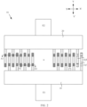
- the electronic device 100 may include a transceiver 101, a memory 102, and a processor 103 (which may be a local processor or a cloud processor), where a filter 1010 is disposed in the transceiver 101, and the filter 1010 is constructed by using a resonator.
- the electronic device may be a television, a mobile phone, a satellite communication device, or a cable television.
- a piston suppression structure is disposed on a surface of the interdigital electrode, so that there is a small quantity of spurious modes between a resonance point and an anti-resonance point, thereby reducing ripples in a passband of the filter constructed by the resonator.
- the resonator in this application may be a surface acoustic wave resonator (that is, a SAW resonator). The following embodiments are described by using this as an example.
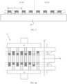
- the resonator includes a piezoelectric substrate 200 and an interdigital transducer 01 disposed on the piezoelectric substrate 200.
- the interdigital transducer 01 includes a plurality of interdigital electrodes T disposed in parallel in a first direction XX', where the plurality of interdigital electrodes include a first interdigital electrode 11 and a second interdigital electrode 12 that are alternately disposed in sequence, and a second bus bar (that is, a second bus bar) 20 and a first bus bar (that is, a first bus bar) 10 are respectively disposed on upper and lower sides of the plurality of interdigital electrodes T in a second direction YY' (that is, perpendicular to the first direction XX'), where lower end portions of all first interdigital electrodes 11 are connected to the first bus bar 10, and upper end portions of all second interdigital electrodes 12 are connected to the second bus bar 20.
- the first interdigital electrode 11 and the second interdigital electrode 12 are periodically, repeatedly, and alternately disposed.
- An arrangement period of the first interdigital electrode 11 and the second interdigital electrode 12 may be basically the same as a wavelength ⁇ of a surface acoustic wave generated by the interdigital transducer 01, that is, a distance between two adjacent interdigital electrodes connected to a same bus bar is equal to the wavelength ⁇ (refer to FIG. 3 ).
- ⁇ in the following refers to a wavelength of a surface acoustic wave generated by the interdigital transducer 01. Details are not described in the following.
- a first piston suppression structure that is, a first piston
- a second piston suppression structure that is, a second piston
- a third piston suppression structure that is, a third piston
- a fourth piston suppression structure that is, a fourth piston
- the first piston 1 is close to the first bus bar 10 relative to the second piston
- the third piston 3 is close to the first bus bar 10 relative to the fourth piston 4. That is, the first piston 1 and the third piston 3 are located on a same side end of the interdigital electrode, and the second piston 2 and the fourth piston 4 are located on a same side end of the interdigital electrode.
- FIG. 2 is merely an example in which a first piston 1 and a second piston 2 are disposed on an upper surface of each first interdigital electrode 11, and a third piston 3 and a fourth piston 4 are disposed on an upper surface of each second interdigital electrode 12.
- this application is not limited thereto.
- the first piston 1 and the second piston 2 may be disposed only on an upper surface of a part of the interdigital electrode 11, and the third piston 3 and the fourth piston 4 may be disposed on an upper surface of a part of the second interdigital electrode 12.
- the first piston 1 and the third piston 3 have different lengths
- the second piston 2 and the fourth piston 4 have different lengths.
- a length of the first piston 1 is less than a length of the third piston 3, and a length of the fourth piston 4 is less than a length of the second piston 2.
- a length of the first piston 1 is greater than a length of the third piston 3, and a length of the fourth piston 4 is greater than a length of the second piston 2.
- the pistons (1, 2, 3, 4) are disposed, so that the resonator can generate a relatively small sound speed (v) at a position (y) at which the piston is disposed on the interdigital electrodes (1, 2), to form a low sound speed region.
- the first piston 1 and the third piston 3 are disposed to have different lengths, two different low sound speed regions (s1, s2) can be formed in a region in which the pistons (1, 3) are disposed on a side of the interdigital electrodes (1, 2) close to the first bus bar 10.
- the second piston 2 and the fourth piston 4 are disposed to have different lengths, two different low sound speed regions (s3, s4) can be formed in a region in which the pistons (2, 4) are disposed on a side of the interdigital electrodes (1, 2) close to the second bus bar 20.
- the low sound speed region is formed on two sides in a direction perpendicular to the wave propagation (that is, a transverse direction), so that resonance formed by reflection of the transverse wave between the first bus bar 10 and the second bus bar 20 can be suppressed (that is, a transverse mode wave is suppressed), and the spurious mode of the resonator between the resonance point and the anti-resonance point are reduced, thereby reducing ripples in the passband of the filter.
- a first electrode E1 connected to the first bus bar 10 and a second electrode E2 connected to the second bus bar 20 may be further disposed.
- the first electrode E1 applies an electrical signal to the first interdigital electrode 11 through the first bus bar 10
- the second electrode E2 applies the electrical signal to the second interdigital electrode 12 through the second bus bar 20, to implement conversion between acoustic signals and electrical signals.
- the first interdigital electrode 11 and the second interdigital electrode 12 may be obtained by using a same metal thin film through patterning.
- the first interdigital electrode 11 and the second interdigital electrode 12 are disposed on a same layer and made of a same material.
- the first interdigital electrode 11 and the second interdigital electrode 12 may use one or more of materials such as aluminum (Al), an Al-based material (for example, AlCu and AlMg), copper (Cu), a Cu-based material, chromium (Cr), silver (Ag), gold (Au), platinum (Pt), or titanium (Ti), and a thickness of the first interdigital electrode 11 and a thickness of the second interdigital electrode 12 may be in a range of 0.01 ⁇ , to 0.2 ⁇ .
- the metal thin film forming the first interdigital electrode 11 and the second interdigital electrode 12 may be a single-layer metal thin film made of one material, or may be a composite metal thin film made of two or more materials. This is not limited in this application, and may be set according to a requirement in practice.
- patterning herein may refer to a process including metal film layer deposition, photoresist coating, exposure, development, etching, and stripping (which may also be referred to as an etching process for short), to implement preparation of a pattern layer including the first interdigital electrode 11 and the second interdigital electrode 12, alternatively, “patterning” may refer to a process may include a process including photoresist coating, exposure, development, metal film layer deposition, and stripping (which may also be referred to as a stripping process for short), to implement preparation of a pattern layer including the first interdigital electrode 11 and the second interdigital electrode 12, which are not limited in this application.
- a proper patterning manufacturing process may be selected according to an actual requirement. This is the same as “patterning” in the following, and details are not described again.
- the first piston 1, the second piston 2, the third piston 3, and the fourth piston 4 may be obtained by using a same thin film through patterning.
- the first piston 1, the second piston 2, the third piston 3, and the fourth piston 4 are disposed on a same layer and made of a same material.
- the first piston 1, the second piston 2, the third piston 3, and the fourth piston 4 may be made of a metal material, or may be made of a non-metal material.
- the metal material may be made of one of aluminum (Al), an Al-based material (for example, AlCu and AlMg), copper (Cu), a Cu-based material, chromium (Cr), silver (Ag), gold (Au), platinum (Pt), or titanium (Ti).
- the non-metal material may be one or more of silicon dioxide (SiO 2 ), silicon nitride (Si x N y ), aluminum oxide (Al x O y ), tantalum oxide (Ta 2 O 5 ), or pyridine oxide (Hf x O y ).
- a thin film forming the first piston 1, the second piston 2, the third piston 3, and the fourth piston 4 may be a single-layer thin film formed by using one material, or may be a composite thin film formed by using two or more materials. This is not limited in this application, and may be set according to a requirement in practice.
- the first bus bar 10, the second bus bar 20, the first electrode E1, and the second electrode E2 may be obtained by patterning a same metal thin film as the first interdigital electrode 11 and the second interdigital electrode 12.
- the first interdigital electrode 11, the second interdigital electrode 12, the first bus bar 10, the second bus bar 20, the first electrode E1, and the second electrode E2 are disposed on the same layer and made of the same material.
- the first bus bar 10, the second bus bar 20, the first electrode E1, and the second electrode E2 may use a structure of two or more metal layers (that is, obtained by patterning a plurality of metal thin film layers).
- the first bus bar 10, the second bus bar 20, the first electrode E1, and the second electrode E2 may be made of an upper and lower two-layer metal structure.
- the lower layer metal structure is obtained by using a same metal film as the first interdigital electrode 11 and the second interdigital electrode 12 by patterning
- the upper layer metal structure is obtained by using a same metal thin film as the first piston 1, the second piston 2, the third piston 3, and the fourth piston 4 by patterning.
- the first interdigital electrode and the second interdigital electrode that are alternately disposed in the interdigital transducer are located on end surfaces on a same side, and pistons of different lengths are alternately disposed, so that two low sound speed regions can be respectively formed at two ends of the first interdigital electrode and the second interdigital electrode that are close to the first bus bar and the second bus bar, and resonance formed by reflection of the transverse wave between the first bus bar and the second bus bar can be suppressed, the clutter between the resonance point and the anti-resonance point of the resonator is reduced, and the ripples in the passband of the filter are reduced.
- a length of the first piston 1 is the same as a length of the fourth piston 4, and a length of the second piston 2 is the same as a length of the third piston 3, to improve a transverse wave suppression effect.
- the lengths of the pistons (1, 2, 3, 4) refer to sizes of the pistons in a second direction YY'.
- a length of the first piston 1 and a length of the fourth piston 4 may be in a range of 0.1 ⁇ to 1 ⁇
- a length of the second piston 2 and a length of the third piston 3 may be in a range of 0.1 ⁇ to 1 ⁇ .
- a setting parameter for example, a length, a material, and a thickness, of each piston may be adjusted, to achieve an objective of optimizing a harmonic suppression effect.
- a thickness t piston of the piston may be set to 10% to 30% of a thickness t IDT of the interdigital electrode (1, 2).
- t piston 10% ⁇ t IDT to 30% ⁇ t IDT .
- the first piston 1 is flush with an edge of the third piston 3 on a side close to the second bus bar 20, and the second piston 2 is flush with an edge of the fourth piston 4 on a side close to the first bus bar 10.
- the resonator may include a first dummy finger electrode b1 (which may also be referred to as a first dummy or a first dummy finger).
- the first dummy finger electrode b1 is disposed in a gap (gap) region between the second interdigital electrode 12 and the first bus bar 10 and at a position opposite to the second interdigital electrode 12, and the first dummy finger electrode b1 is connected to the first bus bar 10.
- a gap gap
- the resonator can further form a low sound speed region (s5) in a setting region of the first dummy finger electrode b1, to further suppress a transverse wave leakage in a direction towards the first bus bar 10, and improve the suppression of the transverse wave.
- s5 low sound speed region
- the resonator may also be a second dummy finger electrode b2 (which may also be referred to as a second dummy or a second dummy finger).
- the second dummy finger electrode b2 is disposed in a gap (gap) region between the first interdigital electrode 11 and the second bus bar 20 and at a position opposite to the first interdigital electrode 11, and the second dummy finger electrode b2 is connected to the second bus bar 20.
- the resonator can further form a low sound speed region (s6) in a setting region of the second dummy finger electrode b2, to further suppress the transverse wave leakage in a direction towards the second bus bar 20, and improve the suppression of the transverse wave.
- the first dummy finger electrode b1 and the second dummy finger electrode b2 are disposed, so that the resonator forms low sound speed regions (s5, s6) in a setting region of the first dummy finger electrode b1 and the second dummy finger electrode b2, to further suppress leakage of a transverse wave in the direction of the first bus bar 10 and the second bus bar 20, thereby improving suppression of the transverse wave and reducing ripples in the passband of the filter.
- the suppression effect of the transverse harmonic leakage close to the anti-resonance point is especially obvious.
- the first dummy finger electrode b1 and the second dummy finger electrode b2 may be disposed to be obtained by using a same metal thin film as the first interdigital electrode 11 and the second interdigital electrode 12 through patterning.
- the first interdigital electrode 11, the second interdigital electrode 12, the first dummy finger electrode b1, and the second dummy finger electrode b2 are disposed on the same layer and made of the same material.
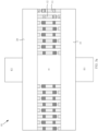
- the surface acoustic wave resonator may further include a reflective structure 02 that is disposed on the piezoelectric substrate 200 and that is respectively located on two sides of the interdigital transducer 01 in the first direction XX', to reflect a surface acoustic wave through the reflective structure 02 on the two sides, so that the surface acoustic wave is restricted between the two reflective structures 02, thereby improving a quality factor (that is, a Q factor and a Q value) of the surface acoustic wave resonator.
- a reflective structure 02 that is disposed on the piezoelectric substrate 200 and that is respectively located on two sides of the interdigital transducer 01 in the first direction XX', to reflect a surface acoustic wave through the reflective structure 02 on the two sides, so that the surface acoustic wave is restricted between the two reflective structures 02, thereby improving a quality factor (that is, a Q factor and a Q value) of the surface acoustic wave resonator.
- the reflective structure 02 may include a plurality of reflective electrodes r disposed in parallel with the interdigital electrodes (11, 12) in the first direction XX', and a first reflective bus bar 21 and a second reflective bus bar 22 that are located at two ends of the reflective electrode r in the second direction YY', where the first reflective bus bar 21 and the first bus bar 10 are located on a same side, and the second reflective bus bar 22 and the second bus bar 20 are located on a same side.
- a manner of disposing the reflective electrode r and a manner of connecting the reflective electrode r to the reflective bus bars (21, 22) may be specifically set according to a requirement.
- the following provides the reflective structure 02 with three different structures.
- a plurality of reflective electrodes r are disposed in parallel in the first direction XX', and two ends of the plurality of reflective electrodes r in the second direction YY' are respectively connected to the first reflective bus bar 21 and the second reflective bus bar 22.
- the plurality of reflective electrodes r disposed in parallel in the first direction XX' include a first reflective electrode r1 and a second reflective electrode r2 that are alternately disposed in sequence, and a boundary reflective electrode r' located on an outermost side in a direction away from the interdigital transducer 01.
- the first reflective electrode r1 is connected to the first reflective bus bar 21, the second reflective electrode r2 is connected to the second reflective bus bar 22, and two ends of the boundary reflective electrode r' are respectively connected to the first reflective bus bar 21 and the second reflective bus bar 22.
- the disposing of the first reflective electrode r1 and the second reflective electrode r2 is equivalent to continuing a manner of disposing the first interdigital electrode 11 and the second interdigital electrode 12.
- the reflective structure 02 further includes a first dummy finger reflective electrode c1 and a second dummy finger reflective electrode c2.
- the first dummy finger reflective electrode c1 is disposed in a gap region between the second reflective electrode r2 and the first reflective bus bar 21 and at a position opposite to the second reflective electrode r2, and the first dummy finger reflective electrode c1 is connected to the first reflective bus bar 21.
- the second dummy finger reflective electrode c2 is disposed at a gap between the first reflective electrode r1 and the second reflection bus bar 22, and at a position opposite to the first reflective electrode r1, and the second dummy finger reflective electrode c2 is connected to the second reflective bus bar 22.
- the first dummy finger reflective electrode c1 continues to be disposed in a manner of the first dummy finger electrode b1
- the second dummy finger reflective electrode c2 continues to be disposed in a manner of the second dummy finger electrode b2.
- a reflective piston d may be respectively disposed on upper surfaces (that is, surfaces on a side away from the piezoelectric substrate 200) of two ends of the reflective electrode r.
- two adjacent reflective pistons of the reflective electrode r on a side close to the first reflective bus bar 21 are respectively a first reflective piston 51 and a third reflective piston 53
- the reflective pistons on a side close to the second reflective bus bar 22 are respectively a second reflective piston 52 and a fourth reflective piston 54.
- the first reflective piston 51 and the second reflective piston 52 are located on upper surfaces of two ends of a same reflective electrode r
- the third reflective piston 53 and the fourth reflective piston 54 are located on upper surfaces of two ends of the same reflective electrode r.
- a reflective piston (a first reflective piston 51 and a third reflective piston 53) located on a side of the reflective electrode r close to the first reflective bus bar 21 is disposed in a same manner as the first piston 1 and the third piston 3.
- the first reflective piston 51 and the first piston 1 are disposed in the same manner (which may include the shape, the size, a position in the second direction YY')
- the third reflective piston 53 and the third piston 3 are disposed in the same manner (which may include the shape, the size, a position in the second direction YY').
- a reflective piston located on a side of the reflective electrode r close to the second reflective bus bar 22 is disposed in the same manner as the second reflective piston 2 and the fourth reflective piston 4.
- the second reflective piston 52 and the second reflective piston 2 are disposed in the same manner (which may include the shape, the size, a position in the second direction YY')
- the fourth reflective piston 54 and the fourth piston 4 are disposed in the same manner (which may include the shape, the size, a position in the second direction YY').
- FIG. 10 is merely an example of the reflective structure 02 shown in the disposing manner 3, but this application is not limited thereto.
- the reflective structure 02 in the disposing manner 1 and disposing manner 2 may also be set according to the disposing manner of the reflective piston d shown in FIG. 10 . Details are not described herein again.
- the reflective electrode r, the first reflective bus bar 21, the second reflective bus bar 22, the first dummy finger reflective electrode c1, and the second dummy finger reflective electrode c2 in the foregoing reflective structure 02 may be obtained by using a same metal thin film as the first interdigital electrode 11 and the second interdigital electrode 12 by patterning.
- the first interdigital electrode 11, the second interdigital electrode 12, the reflective electrode r, the first reflective bus bar 21, the second reflective bus bar 22, the first dummy finger reflective electrode c1, and the second dummy finger reflective electrode c2 are disposed on the same layer and made of the same material.
- the reflective piston d in the foregoing reflective structure 02 may be obtained by using a same thin film as the first piston 1, the second piston 2, the third piston 3, and the fourth piston 4 by patterning.
- the first piston 1, the second piston 2, the third piston 3, the fourth piston 4, and the reflective piston d are disposed on the same layer and made of the same material.
- the piezoelectric substrate 200 may be a single-layer piezoelectric wafer substrate, in other words, the single-layer piezoelectric wafer serves as both a piezoelectric layer and a support substrate.
- the single-layer piezoelectric wafer substrate may be at least one of lithium niobate (LiNbO3) or lithium tantalite (LiTaO 3 ), and a thickness of the single-layer piezoelectric wafer substrate may be in a range of 10 ⁇ m to 1 mm.
- the piezoelectric substrate 200 may be a bonded piezoelectric wafer substrate.
- the piezoelectric layer 220 may be bonded on a Si semiconductor layer 210, and the interdigital transducer 01 is disposed on an upper surface of the piezoelectric layer 220.
- the piezoelectric layer 120 may be one of LiTaO3 or LiNbO3, and a thickness of the piezoelectric layer may be in a range of 1 ⁇ m to 200 ⁇ m.
- the piezoelectric substrate 200 may include a support layer 201, a charge trapping layer 202, a sound speed control layer 203, and a piezoelectric layer 204 that are sequentially disposed in a direction close to the interdigital transducer 01.
- the support layer 201 may be a rigid substrate formed by using one or more of materials such as silicon (Si), silicon carbide (SiC), sapphire (sapphire), quartz (quartz), spinel (spinel), glass (glass), or aluminum oxide (alumina), or may be a flexible substrate formed by using one or more of materials such as PET (polyethylene terephthalate, polyethylene terephthalate), PEN (polyethylene naphthalate, polyethylene naphthalate), PI (polyimide, polyimide), or PES (polyether sulphone, polyether sulphone).
- materials such as silicon (Si), silicon carbide (SiC), sapphire (sapphire), quartz (quartz), spinel (spinel), glass (glass), or aluminum oxide (alumina)
- PET polyethylene terephthalate, polyethylene terephthalate
- PEN polyethylene naphthalate, polyethylene naphthalate
- PI polyimide, polyimide
- the foregoing support layer 201 may be silicon (Si), and a thickness of the support layer 201 may be in a range of 10 ⁇ m to 1 mm.
- the foregoing charge trapping layer 202 may be made of a material that can perform charge fixing, to reduce radio frequency leakage of the resonator.
- the charge trapping layer 202 may use a special form of silicon (Si)-based material, for example, amorphous Si or nanocrystalline Si, and a thickness of the charge trapping layer 202 may be in a range of 100 nm to 10 ⁇ m.
- Si silicon
- the foregoing sound speed control layer 203 may be a single-layer low sound speed control layer, or may be a two-layer or multi-layer structure in which a high sound speed control layer and a low sound speed control layer are alternately combined.
- a material for forming the sound speed control layer 203 may include one or more of materials such as silicon dioxide (SiO 2 ), silicon nitride (Si x N y ), aluminum nitride (AlN), scandium aluminum nitride (ScAlN), tantalum oxide (Ta 2 O 5 ), tantalum (Ta), pyridine oxide (Hf x O y ), tungsten (W), platinum (Pt), or bait (Ir).
- the sound speed control layer 203 may be a single-layer structure formed by using one material, or may be a composite layer formed by using two or more materials.
- the sound speed control layer 203 may use silicon dioxide (SiO 2 ), and a thickness of the sound speed control layer 203 may be in a range of 10 nm to 10 ⁇ m.
- the foregoing piezoelectric layer 204 may be made of a material such as lithium niobate (LiNbO3), lithium tantalumate (LiTaO 3 ), quartz (quartz), aluminum nitride (AlN), scandium aluminum nitride (ScAlN), PZT (lead zirconate titanate, lead zirconate titanate) piezoelectric ceramic, zinc oxide (ZnO), or a PMN-PT-based material (that is, a PMN-PT - lead titanate piezoelectric material), and the piezoelectric layer 204 may be a single-layer structure formed by using one material, or may be a composite layer formed by using two or more materials.
- a material such as lithium niobate (LiNbO3), lithium tantalumate (LiTaO 3 ), quartz (quartz), aluminum nitride (AlN), scandium aluminum nitride (ScAlN), PZT
- the piezoelectric layer 204 may be a lithium tantalumate (LiTaO 3 ), and a thickness of the piezoelectric layer 204 may be in a range of 100 nm to 700 ⁇ m.
- an insulating dielectric layer 300 covering a side of the interdigital transducer 01 away from the piezoelectric substrate 200 may be further disposed, to protect a surface of the interdigital transducer 01 through the insulating dielectric layer 300.
- the insulating dielectric layer 300 extends to a surface of the reflective structure 02, to protect the reflective structure 02.
- the insulating dielectric layer 300 may be made of one or more of materials such as silicon dioxide (SiO 2 ), silicon nitride (Si x N y ), aluminum oxide (Al x O y ), tantalum oxide (Ta 2 O 5 ), or pyridium oxide (Hf x O y ), and the insulating dielectric layer 300 may be a single-layer structure formed by using one material, or may be a composite layer formed by using two or more materials.
- materials such as silicon dioxide (SiO 2 ), silicon nitride (Si x N y ), aluminum oxide (Al x O y ), tantalum oxide (Ta 2 O 5 ), or pyridium oxide (Hf x O y )
- the insulating dielectric layer 300 may be a single-layer structure formed by using one material, or may be a composite layer formed by using two or more materials.
- the insulating dielectric layer 300 may be a composite layer formed by using a silicon oxide (SiO 2 ) layer and silicon nitride (Si x N y ) layer.
- a thickness of the SiO 2 layer located at a lower layer is in a range of 5 nm to 50 nm
- a thickness of the Si x N y layer located at an upper layer is in a range of 5 nm to 20 nm.
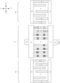
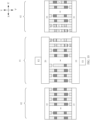
- the SAW resonator provided in embodiments of this application may be a dual mode surface acoustic wave resonator, that is, a DMS resonator (dual mode SAW), or may be referred to as a DMS for short.
- the DMS resonator may include a plurality of interdigital transducers 01 disposed in parallel in a first direction XX', and FIG. 12 is merely an example in which two interdigital transducers 01 are disposed in parallel in a dual mode surface acoustic wave resonator is used for description.
- interdigital transducers 01 may be disposed in parallel, a quantity of interdigital transducers 01 disposed in parallel in the DMS resonator is not limited in this application. In practice, the interdigital transducers 01 may be selectively disposed according to a requirement.
- the DMS resonator may further include a reflective structure 02 respectively located on an outer side of the plurality of interdigital transducers 01 that are disposed in parallel in the first direction XX', to increase a Q factor of the dual mode surface acoustic wave resonator.
- the following uses a resonator shown in FIG. 10 as an example to describe a method for manufacturing the resonator provided in embodiments of this application.
- Step 01. Set a piezoelectric substrate 200.
- the piezoelectric substrate 200 may include a support layer 201, a charge trapping layer 202, a sound speed control layer 203, and a piezoelectric layer 204 that are sequentially disposed from bottom to top, where the support layer 101 may be a silicon (Si) layer with a thickness of 200 ⁇ m to 700 ⁇ m, the charge trapping layer 102 is an amorphous Si layer with a thickness of 100 nm to 10 ⁇ m, the sound speed control layer 103 may be a silicon dioxide (SiO 2 ) layer with a thickness of 300 nm to 2 ⁇ m, and the piezoelectric layer 104 may be a lithium tantalite (LiTaO 3 ) layer with a thickness of 200 nm to 1 ⁇ m.
- the support layer 101 may be a silicon (Si) layer with a thickness of 200 ⁇ m to 700 ⁇ m
- the charge trapping layer 102 is an amorphous Si layer with a thickness of 100 nm to 10 ⁇ m
- Step 02. Form a first metal thin film on a surface of the piezoelectric substrate 200, and pattern the first metal thin film to form a first metal pattern.
- the first metal pattern includes a first interdigital electrode 11, a second interdigital electrode 12, a first dummy finger electrode b1, a second dummy finger electrode b2, a first bus bar 10, a second bus bar 20, a first electrode E1, and a second electrode E2 formed in an interdigital transducer 01, and a first reflective bus bar 21, a second reflective bus bar 22, a reflective electrode r, a first dummy finger reflective electrode c1, and a second dummy finger reflective electrode c2 in a reflective structure 02.
- the first metal thin film may be a Ti/AlCu composite film layer, where a content of Cu is in a range of 0.5% to 2%, a thickness of a Ti layer located at a lower layer may be in a range of 5 nm to 30 nm (for example, may be 20 nm), and a thickness of an AlCu located at an upper layer may be in a range of 0.05 ⁇ to 0.12 ⁇ .
- Step 03. Form a second metal thin film on the first metal pattern (including 1, 2, b1, b2, 10, 20, E1, E2, 21, 22, r, c1, and c2) formed after the first metal thin film is patterned, and pattern the second metal thin film to form a second metal pattern, where the second metal pattern includes a first piston 1, a second piston 2, a third piston 3, a fourth piston 4, and a reflective piston d.
- step 03 when the second metal thin film is patterned, thickening electrodes of the first bus bar 10, the second bus bar 20, the first electrode E1, and the second electrode E2 may be formed at positions corresponding to the first bus bar 10, the second bus bar 20, the first electrode E1, and the second electrode E2.
- the second metal thin film may be a Ti/AlCu composite film layer, where a content of Cu is in a range of 0.5% to 2%, a thickness of a Ti layer located at a lower layer may be in a range of 5 nm to 30 nm (for example, may be 20 nm), and a thickness of an AlCu located at an upper layer may be in a range of 0.5 ⁇ m to 3 ⁇ m.
- a third metal thin film may be formed on the second metal pattern (including 10, 20, E1, and E2) through step 04, and the third metal thin film is patterned to form thickening electrodes of the first bus bar 10, the second bus bar 20, the first electrode E1, and the second electrode E2.
- the third metal thin film may be a Ti/Au composite film layer, a thickness of a Ti layer located at a lower layer may be in a range of 5 nm to 30 nm (for example, may be 20 nm), and a thickness of Au located at an upper layer may be in a range of 0.5 ⁇ m to 3 ⁇ m.
- the first bus bar 10, the second bus bar 20, the first electrode E1, and the second electrode E2 may use a multi-composite layer structure (Ti/AlCu/Ti/AlCu) formed by the first metal thin film (for example, Ti/AlCu) and the second metal thin film (for example, Ti/AlCu), or may use a multi-composite layer structure (Ti/AlCu/Ti/AlCu/Ti/Au) formed by the first metal thin film (for example, Ti/AlCu), the second metal thin film (for example, Ti/AlCu), and the third metal thin film (for example, Ti/Au).
- the method may further include forming an insulating dielectric layer 300 on the second metal pattern formed after the second metal thin film is patterned.
- the insulating dielectric layer 300 may include a SiO 2 layer located at a lower layer and having a thickness of 5 nm to 50 nm, and a Si x N y layer located at an upper layer and having a thickness of 5 nm to 20 nm.
- the filter may be a filter of a ladder (ladder) structure.
- the foregoing SAW resonator may be used to form a ladder filter.
- the filter may include an input end IN, an output end OUT, a series branch B1, and at least one parallel branch B2.
- the series branch B1 is connected between the input end IN and the output end OUT
- one end of the parallel branch B2 is connected to the series branch B1
- the other end of the parallel branch B2 is connected to a ground end
- at least two series resonators for example, Si, S 2 ..., S n
- parallel resonators for example, P 1 , P 2 ..., P n-1
- At least one series resonator (for example, it may be all) in the foregoing series branch B1 may be set to use the resonator provided in any one of the foregoing possible implementations of this application.
- the parallel resonator in the at least one parallel branch B2 may be set to use the resonator provided in any one of the foregoing possible implementations of this application.
- the series resonator in the series branch B1 and the parallel resonator in the parallel branch B2 may be set to use the resonators provided in any one of the foregoing possible implementations of this application.
- the foregoing SAW resonator and the DMS resonator may be used to form a filter.
- the filter may include a plurality of DMS resonators (DMS 1 , DMS 2 ..., DMS n ) disposed in parallel, and the DMS resonators (DMS 1 , DMS 2 ..., DMS n ) disposed in parallel are disposed in series with the ladder filter.
- the filter may be designed according to the resonator provided in embodiments of this application.
Landscapes
- Physics & Mathematics (AREA)
- Acoustics & Sound (AREA)
- Surface Acoustic Wave Elements And Circuit Networks Thereof (AREA)
Applications Claiming Priority (1)
| Application Number | Priority Date | Filing Date | Title |
|---|---|---|---|
| PCT/CN2020/126075 WO2022094743A1 (zh) | 2020-11-03 | 2020-11-03 | 谐振器、滤波器及电子设备 |
Publications (2)
| Publication Number | Publication Date |
|---|---|
| EP4228155A1 true EP4228155A1 (de) | 2023-08-16 |
| EP4228155A4 EP4228155A4 (de) | 2023-12-20 |
Family
ID=81458446
Family Applications (1)
| Application Number | Title | Priority Date | Filing Date |
|---|---|---|---|
| EP20960206.9A Pending EP4228155A4 (de) | 2020-11-03 | 2020-11-03 | Resonator, filter und elektronische vorrichtung |
Country Status (3)
| Country | Link |
|---|---|
| EP (1) | EP4228155A4 (de) |
| CN (1) | CN115989635A (de) |
| WO (1) | WO2022094743A1 (de) |
Families Citing this family (11)
| Publication number | Priority date | Publication date | Assignee | Title |
|---|---|---|---|---|
| CN114978089B (zh) * | 2022-05-20 | 2023-11-21 | 武汉敏声新技术有限公司 | 一种谐振器及其制备方法、滤波器 |
| CN115425941A (zh) * | 2022-07-30 | 2022-12-02 | 锐石创芯(重庆)科技有限公司 | 谐振器、滤波器及电子设备 |
| CN115208349A (zh) * | 2022-09-16 | 2022-10-18 | 深圳新声半导体有限公司 | 一种声表面波滤波器 |
| CN116192085A (zh) * | 2023-02-20 | 2023-05-30 | 无锡市好达电子股份有限公司 | 横向激发体声波谐振器 |
| CN116366022A (zh) * | 2023-03-20 | 2023-06-30 | 江苏卓胜微电子股份有限公司 | 温度补偿声表面换能器及制造方法 |
| CN116683885B (zh) * | 2023-05-23 | 2023-12-22 | 无锡市好达电子股份有限公司 | 一种具有活塞模式的声表面波装置 |
| WO2025087343A1 (zh) * | 2023-10-25 | 2025-05-01 | 锐石创芯(重庆)科技有限公司 | 谐振器、滤波器及射频前端模组 |
| CN117526896B (zh) * | 2023-12-29 | 2024-12-20 | 深圳新声半导体有限公司 | 一种具有抑制杂波单元的tc-saw谐振结构 |
| CN120389723A (zh) * | 2024-01-26 | 2025-07-29 | 华为技术有限公司 | 滤波器、射频芯片及电子设备 |
| CN121602947A (zh) * | 2024-08-15 | 2026-03-03 | 华为技术有限公司 | 声学谐振器、滤波器、射频芯片和电子设备 |
| CN120415367B (zh) * | 2025-07-04 | 2025-08-29 | 深圳新声半导体有限公司 | 一种tf-saw谐振器及其制备方法、滤波器 |
Family Cites Families (13)
| Publication number | Priority date | Publication date | Assignee | Title |
|---|---|---|---|---|
| US7576471B1 (en) * | 2007-09-28 | 2009-08-18 | Triquint Semiconductor, Inc. | SAW filter operable in a piston mode |
| US7939989B2 (en) * | 2009-09-22 | 2011-05-10 | Triquint Semiconductor, Inc. | Piston mode acoustic wave device and method providing a high coupling factor |
| DE102010005596B4 (de) * | 2010-01-25 | 2015-11-05 | Epcos Ag | Elektroakustischer Wandler mit verringerten Verlusten durch transversale Emission und verbesserter Performance durch Unterdrückung transversaler Moden |
| KR102636251B1 (ko) * | 2016-02-24 | 2024-02-14 | (주)와이솔 | 횡모드 억제를 위한 표면 탄성파 디바이스 |
| JP6509151B2 (ja) * | 2016-03-11 | 2019-05-08 | 太陽誘電株式会社 | 弾性波共振器、フィルタおよびマルチプレクサ |
| DE112017003190B4 (de) * | 2016-06-27 | 2025-02-20 | Murata Manufacturing Co., Ltd. | Vorrichtung für elastische Wellen |
| WO2018216548A1 (ja) * | 2017-05-22 | 2018-11-29 | 株式会社村田製作所 | 弾性波装置 |
| JP2019091978A (ja) * | 2017-11-13 | 2019-06-13 | 株式会社村田製作所 | 弾性波装置、高周波フロントエンド回路及び通信装置 |
| DE102018108732B4 (de) * | 2018-04-12 | 2024-10-17 | Rf360 Singapore Pte. Ltd. | Dünnschicht SAW-Wandler mit verbesserten Eigenschaften, elektroakustisches Filter und HF-Filter |
| CN109004914B (zh) * | 2018-07-11 | 2022-05-03 | 开元通信技术(厦门)有限公司 | 一种声表面波器件及其制备方法 |
| DE102018124372A1 (de) * | 2018-10-02 | 2020-04-02 | RF360 Europe GmbH | Elektroakustischer Resonator |
| CN113454911B (zh) * | 2019-02-18 | 2024-05-07 | 株式会社村田制作所 | 弹性波装置 |
| CN110572136B (zh) * | 2019-09-09 | 2022-11-01 | 杭州左蓝微电子技术有限公司 | 一种叉指换能器 |
-
2020
- 2020-11-03 CN CN202080103518.1A patent/CN115989635A/zh active Pending
- 2020-11-03 WO PCT/CN2020/126075 patent/WO2022094743A1/zh not_active Ceased
- 2020-11-03 EP EP20960206.9A patent/EP4228155A4/de active Pending
Also Published As
| Publication number | Publication date |
|---|---|
| CN115989635A (zh) | 2023-04-18 |
| EP4228155A4 (de) | 2023-12-20 |
| WO2022094743A1 (zh) | 2022-05-12 |
Similar Documents
| Publication | Publication Date | Title |
|---|---|---|
| WO2022094743A1 (zh) | 谐振器、滤波器及电子设备 | |
| US12389801B2 (en) | Acoustic wave device | |
| CN109600125B (zh) | 滤波器 | |
| US10826461B2 (en) | Acoustic wave device | |
| US9035725B2 (en) | Acoustic wave device | |
| US9124243B2 (en) | Surface acoustic wave filter device | |
| JP5099151B2 (ja) | 弾性境界波装置の製造方法 | |
| US7567023B2 (en) | Piezoelectric thin-film resonator and filter using the same | |
| US11309866B2 (en) | Acoustic wave device and method for manufacturing acoustic wave device | |
| EP1914888A1 (de) | Abzweigfilter | |
| US11996828B2 (en) | Filter device | |
| CN114070257B (zh) | 声波装置、滤波器及多路复用器 | |
| US12278613B1 (en) | Surface acoustic wave resonator device, manufacturing method therefore and filter | |
| US20250175141A1 (en) | Acoustic wave device | |
| US11936359B2 (en) | Acoustic wave device and multiplexer | |
| US20220239280A1 (en) | Acoustic wave filter | |
| US8564173B2 (en) | Elastic wave device | |
| US12574015B2 (en) | Multiplexer | |
| JP2021136558A (ja) | フィルタおよびマルチプレクサ | |
| US20240275354A1 (en) | Acoustic wave device | |
| JP2025146093A (ja) | 弾性波デバイス、フィルタ、マルチプレクサ、及び弾性波デバイスの製造方法 | |
| WO2023068206A1 (ja) | マルチプレクサ | |
| CN119137862A (zh) | 表面声波谐振器元件和包括所述表面声波谐振器元件的电子装置 | |
| CN116671008A (zh) | 滤波器以及多工器 |
Legal Events
| Date | Code | Title | Description |
|---|---|---|---|
| STAA | Information on the status of an ep patent application or granted ep patent |
Free format text: STATUS: THE INTERNATIONAL PUBLICATION HAS BEEN MADE |
|
| PUAI | Public reference made under article 153(3) epc to a published international application that has entered the european phase |
Free format text: ORIGINAL CODE: 0009012 |
|
| STAA | Information on the status of an ep patent application or granted ep patent |
Free format text: STATUS: REQUEST FOR EXAMINATION WAS MADE |
|
| 17P | Request for examination filed |
Effective date: 20230509 |
|
| AK | Designated contracting states |
Kind code of ref document: A1 Designated state(s): AL AT BE BG CH CY CZ DE DK EE ES FI FR GB GR HR HU IE IS IT LI LT LU LV MC MK MT NL NO PL PT RO RS SE SI SK SM TR |
|
| REG | Reference to a national code |
Ref country code: DE Ref legal event code: R079 Free format text: PREVIOUS MAIN CLASS: H03H0009020000 Ipc: H03H0009145000 |
|
| A4 | Supplementary search report drawn up and despatched |
Effective date: 20231116 |
|
| RIC1 | Information provided on ipc code assigned before grant |
Ipc: H03H 9/64 20060101ALI20231110BHEP Ipc: H03H 9/02 20060101ALI20231110BHEP Ipc: H03H 9/145 20060101AFI20231110BHEP |
|
| DAV | Request for validation of the european patent (deleted) | ||
| DAX | Request for extension of the european patent (deleted) |