EP4230761B1 - Verfahren zur reaktiven magnetron-sputterbeschichtung von galliumoxid-dünnschichten - Google Patents
Verfahren zur reaktiven magnetron-sputterbeschichtung von galliumoxid-dünnschichten Download PDFInfo
- Publication number
- EP4230761B1 EP4230761B1 EP22195507.3A EP22195507A EP4230761B1 EP 4230761 B1 EP4230761 B1 EP 4230761B1 EP 22195507 A EP22195507 A EP 22195507A EP 4230761 B1 EP4230761 B1 EP 4230761B1
- Authority
- EP
- European Patent Office
- Prior art keywords
- sputtering
- layer
- gallium
- deposition
- target
- Prior art date
- Legal status (The legal status is an assumption and is not a legal conclusion. Google has not performed a legal analysis and makes no representation as to the accuracy of the status listed.)
- Active
Links
Images


Classifications
-
- C—CHEMISTRY; METALLURGY
- C23—COATING METALLIC MATERIAL; COATING MATERIAL WITH METALLIC MATERIAL; CHEMICAL SURFACE TREATMENT; DIFFUSION TREATMENT OF METALLIC MATERIAL; COATING BY VACUUM EVAPORATION, BY SPUTTERING, BY ION IMPLANTATION OR BY CHEMICAL VAPOUR DEPOSITION, IN GENERAL; INHIBITING CORROSION OF METALLIC MATERIAL OR INCRUSTATION IN GENERAL
- C23C—COATING METALLIC MATERIAL; COATING MATERIAL WITH METALLIC MATERIAL; SURFACE TREATMENT OF METALLIC MATERIAL BY DIFFUSION INTO THE SURFACE, BY CHEMICAL CONVERSION OR SUBSTITUTION; COATING BY VACUUM EVAPORATION, BY SPUTTERING, BY ION IMPLANTATION OR BY CHEMICAL VAPOUR DEPOSITION, IN GENERAL
- C23C14/00—Coating by vacuum evaporation, by sputtering or by ion implantation of the coating forming material
- C23C14/06—Coating by vacuum evaporation, by sputtering or by ion implantation of the coating forming material characterised by the coating material
- C23C14/08—Oxides
-
- C—CHEMISTRY; METALLURGY
- C23—COATING METALLIC MATERIAL; COATING MATERIAL WITH METALLIC MATERIAL; CHEMICAL SURFACE TREATMENT; DIFFUSION TREATMENT OF METALLIC MATERIAL; COATING BY VACUUM EVAPORATION, BY SPUTTERING, BY ION IMPLANTATION OR BY CHEMICAL VAPOUR DEPOSITION, IN GENERAL; INHIBITING CORROSION OF METALLIC MATERIAL OR INCRUSTATION IN GENERAL
- C23C—COATING METALLIC MATERIAL; COATING MATERIAL WITH METALLIC MATERIAL; SURFACE TREATMENT OF METALLIC MATERIAL BY DIFFUSION INTO THE SURFACE, BY CHEMICAL CONVERSION OR SUBSTITUTION; COATING BY VACUUM EVAPORATION, BY SPUTTERING, BY ION IMPLANTATION OR BY CHEMICAL VAPOUR DEPOSITION, IN GENERAL
- C23C14/00—Coating by vacuum evaporation, by sputtering or by ion implantation of the coating forming material
- C23C14/0021—Reactive sputtering or evaporation
- C23C14/0036—Reactive sputtering
-
- C—CHEMISTRY; METALLURGY
- C23—COATING METALLIC MATERIAL; COATING MATERIAL WITH METALLIC MATERIAL; CHEMICAL SURFACE TREATMENT; DIFFUSION TREATMENT OF METALLIC MATERIAL; COATING BY VACUUM EVAPORATION, BY SPUTTERING, BY ION IMPLANTATION OR BY CHEMICAL VAPOUR DEPOSITION, IN GENERAL; INHIBITING CORROSION OF METALLIC MATERIAL OR INCRUSTATION IN GENERAL
- C23C—COATING METALLIC MATERIAL; COATING MATERIAL WITH METALLIC MATERIAL; SURFACE TREATMENT OF METALLIC MATERIAL BY DIFFUSION INTO THE SURFACE, BY CHEMICAL CONVERSION OR SUBSTITUTION; COATING BY VACUUM EVAPORATION, BY SPUTTERING, BY ION IMPLANTATION OR BY CHEMICAL VAPOUR DEPOSITION, IN GENERAL
- C23C14/00—Coating by vacuum evaporation, by sputtering or by ion implantation of the coating forming material
- C23C14/22—Coating by vacuum evaporation, by sputtering or by ion implantation of the coating forming material characterised by the process of coating
- C23C14/34—Sputtering
- C23C14/3407—Cathode assembly for sputtering apparatus, e.g. Target
-
- C—CHEMISTRY; METALLURGY
- C23—COATING METALLIC MATERIAL; COATING MATERIAL WITH METALLIC MATERIAL; CHEMICAL SURFACE TREATMENT; DIFFUSION TREATMENT OF METALLIC MATERIAL; COATING BY VACUUM EVAPORATION, BY SPUTTERING, BY ION IMPLANTATION OR BY CHEMICAL VAPOUR DEPOSITION, IN GENERAL; INHIBITING CORROSION OF METALLIC MATERIAL OR INCRUSTATION IN GENERAL
- C23C—COATING METALLIC MATERIAL; COATING MATERIAL WITH METALLIC MATERIAL; SURFACE TREATMENT OF METALLIC MATERIAL BY DIFFUSION INTO THE SURFACE, BY CHEMICAL CONVERSION OR SUBSTITUTION; COATING BY VACUUM EVAPORATION, BY SPUTTERING, BY ION IMPLANTATION OR BY CHEMICAL VAPOUR DEPOSITION, IN GENERAL
- C23C14/00—Coating by vacuum evaporation, by sputtering or by ion implantation of the coating forming material
- C23C14/22—Coating by vacuum evaporation, by sputtering or by ion implantation of the coating forming material characterised by the process of coating
- C23C14/34—Sputtering
- C23C14/3407—Cathode assembly for sputtering apparatus, e.g. Target
- C23C14/3428—Cathode assembly for sputtering apparatus, e.g. Target using liquid targets
-
- H—ELECTRICITY
- H01—ELECTRIC ELEMENTS
- H01J—ELECTRIC DISCHARGE TUBES OR DISCHARGE LAMPS
- H01J37/00—Discharge tubes with provision for introducing objects or material to be exposed to the discharge, e.g. for the purpose of examination or processing thereof
- H01J37/32—Gas-filled discharge tubes
- H01J37/34—Gas-filled discharge tubes operating with cathodic sputtering
- H01J37/3402—Gas-filled discharge tubes operating with cathodic sputtering using supplementary magnetic fields
- H01J37/3405—Magnetron sputtering
-
- H—ELECTRICITY
- H01—ELECTRIC ELEMENTS
- H01J—ELECTRIC DISCHARGE TUBES OR DISCHARGE LAMPS
- H01J37/00—Discharge tubes with provision for introducing objects or material to be exposed to the discharge, e.g. for the purpose of examination or processing thereof
- H01J37/32—Gas-filled discharge tubes
- H01J37/34—Gas-filled discharge tubes operating with cathodic sputtering
- H01J37/3411—Constructional aspects of the reactor
- H01J37/3414—Targets
- H01J37/3426—Material
-
- H—ELECTRICITY
- H01—ELECTRIC ELEMENTS
- H01J—ELECTRIC DISCHARGE TUBES OR DISCHARGE LAMPS
- H01J37/00—Discharge tubes with provision for introducing objects or material to be exposed to the discharge, e.g. for the purpose of examination or processing thereof
- H01J37/32—Gas-filled discharge tubes
- H01J37/34—Gas-filled discharge tubes operating with cathodic sputtering
- H01J37/3488—Constructional details of particle beam apparatus not otherwise provided for, e.g. arrangement, mounting, housing, environment; special provisions for cleaning or maintenance of the apparatus
- H01J37/3491—Manufacturing of targets
Definitions
- This invention relates to a method of reactive magnetron sputtering deposition of Ga 2 O 3 thin films from a metallic target.
- Ga 2 O 3 can crystallize in five different phases. While the most stable and technologically relevant is the monoclinic ⁇ phase [1], there is an increasing interest in the other phases [2,3] and amorphous Ga 2 O 3 coatings [4] as well.
- the properties of technological importance include transparency in the UV part of the spectrum due to its wide band gap of approximately 5 eV, decent carrier mobility ( ⁇ 100 cm 2 /Vs), high breakdown field (8 MV/cm), and high thermal and chemical stability.
- Practical applications include high-voltage transistors, high-power Schottky diodes, high-temperature chemical sensors, and transparent conductive oxides in devices requiring high transmittance in the short wavelength part of the spectrum [1,5].
- Ga 2 O 3 thin film deposition includes MOCVD [7], ALD [8], PLD [9], e-beam evaporation [4], aqueous solution deposition [10], and RF magnetron sputtering from ceramic Ga 2 O 3 targets [11,12-17].
- MOCVD MOCVD
- ALD ALD
- PLD PLD
- 9 e-beam evaporation
- aqueous solution deposition RF magnetron sputtering from ceramic Ga 2 O 3 targets [11,12-17].
- the deposition rate of sputter-deposited films has been reported to depend on the substrate temperature as well.
- the films on 800°C sapphire substrates were deposited at 1 nm/min [12-15], in sharp contrast with the rate of 15 - 22 nm/min for films deposited onto unheated glass substrates [11].
- a deposition rate decreases from approximately 20 to less than 10 nm/min upon silicon substrate temperature increase from 100 to 600 °C was reported in [
- the subject of the invention is gallium oxide thin films coatings deposited by reactive DC magnetron sputtering from metallic gallium target.
- the deposition rate - up to 41 nm/min at room temperature on quartz and 5 nm/min at 800 °C on sapphire - is higher than the literature data for RF sputtering (22 and 1 nm/min, respectively).
- Amorphous and crystalline films have been deposited depending on the substrate temperature.
- a feature in XRD spectrum is present that may be indicative of the presence of small size crystallites of ⁇ -Ga 2 O 3 in a predominantly amorphous film.
- ⁇ -Ga 2 O 3 of single orientation was detected on sapphire, a mix of different orientations detected on quartz.
- the film structure dependence on the temperature is consistent with the literature data for other methods of deposition.
- US2015/0060262 [17] describes a sputtering system with a liquid target (which can be gallium) depositing on a second rotatable solid target (which can be indium), the two materials being co-sputtered on a substrate.
- thin film in this description refers to a surface coating with the thickness in the range from 50 to 2500 nm.
- the goal of the invention is to provide a method for deposition of gallium oxide on a substrate.
- the set goal is reached by the proposed method for deposition of gallium oxide on a substrate inside a vacuum chamber by reactive direct current magnetron sputtering device, wherein the method comprises the following steps: (i) placing metallic gallium pellets into a stain less steel container; (ii) heating the target container for the pellets to melt and form a uniform layer prior to mounting to the magnetron, to be the target in a liquid state during the sputtering; (iii) positioning the target in a vacuum chamber with the to serve as the source of sputtered particles; (iv) sputter-depositing an oxide film by reactive magnetron sputtering in argon/oxygen atmosphere; the base pressure in a turbomolecular pumped chamber preferably from 10 -7 to 10 -5 Torr and the process pressure preferably from 1.0 to 15.0 mTorr; the front surface of the target container is precoated by an
- the Oxygen flow during the sputtering is controlled by Plasma optical emission spectroscopy keeping the intensity of gallium 417,2 nm emission line constant at the level ensuring the deposition of an optically transparent film onto the substrate.
- the melting temperature of metallic gallium is 29,8 °C.
- the adhesion promoting layer allows a continuous layer of gallium to form and to withstand repeated deposition cycles without exposing the container base to sputtering.
- the front surface of the target container is precoated by a thin adhesion promoting layer of SiO 2 . Since SiO 2 is electrically insulating, the electrical contact between the target container and the Gallium target is provided by a set of erosion-zone-shaped lines etched through the SiO 2 layer.
- the substrate is quartz or c-sapphire with the substrate temperature varied between room, i.e., no intentional heating provided, and 800 °C.
- the deposition rate for optically transparent films is up to 41 nm/min at room temperature on quartz and 5 nm/min at 800 °C on sapphire.
- the time of the deposition is selected so to achieve the necessary thickness of the deposited film.
- the goal of the invention is to provide a method for deposition of thin films of gallium oxide on a substrate.
- the set goal is reached by the proposed method for deposition of gallium oxide on a substrate inside a vacuum chamber by reactive magnetron sputtering device, wherein the method comprises the following steps: (i) placing metallic gallium pellets into a stainless steel container; (ii) heating the target container for the pellets to melt and form a uniform layer prior to mounting to the magnetron, to be the target in a liquid state during the sputtering; (iii) positioning the target in a vacuum reaction chamber having a magnetron as the source for sputtered particles; (iv) depositing a film by sputtering the metal target in argon/oxygen atmosphere; (v) locking the sputtering process into PID control mode, keeping the intensity of gallium 417.2 nm emission line constant during the deposition of the film onto the substrate.
- the target was prepared by placing metallic gallium pellets into a 15.0 x 7.5 cm box-shaped stainless steel container with 3 mm high sides. The container was heated for the pellets to melt and form a uniform layer prior to mounting to the magnetron. With the melting temperature of gallium being 29,8 degrees Celsius, the target was in a liquid state during the sputtering.
- the second design tested was a container with a machined recess in the base plane ( Fig. 1 ), the recess was erosion zone shaped and wider than the actual erosion zone. Although an improvement, this still led to minor - approximately 0,5 cm 2 large - uncovered areas of the base of the container randomly distributed along the perimeter of the erosion zone developed during the sputtering.
- the container of Fig. 1 was tested with the top surface sputter-precoated by a thin layer of Ga 2 O 3 , SiO 2 or carbon. Since SiO 2 is electrically insulating, the electrical contact between the target container and the Gallium target was provided by a set of erosion-zone-shaped lines etched through the SiO 2 layer. While the layer of Ga 2 O 3 did not lead to any improvement, the layers of Carbon and SiOz enhanced the adhesion substantially, allowing a continuous layer of gallium to form and to withstand repeated deposition cycles without exposing the container base to sputtering.
- the sputtering was carried out in DC mode in argon/oxygen atmosphere at 100 to 250 W power.
- the same magnetron cooling system was used as for ordinary solid targets, i.e., the magnetron was cooled by 20°C water flow.
- the base pressure was 10 -6 Torr in a turbomolecular pumped chamber.
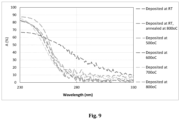
- the process pressure was set at 3 mTorr by feeding 30 sccm of argon and partly closing the valve between the chamber and the pump. Quartz and c-sapphire substrates were used, with the substrate temperature varied between room (i.e., no intentional heating provided) and 800°C. Selected samples deposited at room temperature were later annealed at 800°C in air to determine whether there is a detectable difference in properties between the films heated during or after the deposition.
- the process control was done by Optical Emission Spectroscopy (OES), i.e., the oxygen flow was controlled by a feedback loop keeping the intensity of gallium 417,2 nm emission line constant.
- OES Optical Emission Spectroscopy
- An example of a typical deposition run is provided in Fig. 2 .
- the process is started in the metal mode (argon only), the emission line intensity denoted I met .
- Oxygen is added and the flow is increased manually to reduce the emission line intensity to the desired value.
- the process is locked into PID control mode, keeping the line intensity constant at the set value I proc .
- the shutter is open, and the film is deposited onto the substrate.
- the Oxygen flow during the deposition was approximately 7.8 sccm.
- the film thickness was measured by stylus profilometer (instrument Dektak 150) and ellipsometry (instrument Woollam RC2-XI), both techniques gave similar thickness values.
- the thickness was determined by ellipsometry.
- the film structure was examined by X-ray diffraction, using Rigaku MiniFlex 600 instrument. Optical transmittance and reflectance were measured by Cary 7000 spectrophotometer.
- the deposition rate as a function of normalized gallium emission line intensity I proc /I met upon reactive sputtering from metallic gallium target at varied sputtering power and substrate temperature for films deposited on quartz and sapphire substrates is shown in Figure 3 .
- the highest deposition rate value shown in Figure 3 approximately 51 nm/min, yielded an apparently under oxidized (optically absorbing) coating. For all other points shown in Figure 3 the coatings were highly transparent.
- Described herein is process of deposition of Ga 2 O 3 thin films by reactive DC magnetron sputtering form liquid Gallium metal target.
- the deposition rate - up to 41 nm/min at room temperature on quartz and 5 nm/min at 800°C on sapphire - is higher than the literature data for RF sputtering from ceramic targets (22 and 1 nm/min, respectively).
- Amorphous and crystalline films have been deposited depending on the substrate temperature.
- a feature in XRD spectrum is present that may be indicative of the presence of small size crystallites of ⁇ -Ga 2 O 3 in a predominantly amorphous film.
- ⁇ -Ga 2 O 3 of single orientation was detected on sapphire, a mix of different orientations detected on quartz.
- the film structure dependence on the temperature is consistent with the literature data for other methods of deposition.
Landscapes
- Chemical & Material Sciences (AREA)
- Engineering & Computer Science (AREA)
- Chemical Kinetics & Catalysis (AREA)
- Materials Engineering (AREA)
- Mechanical Engineering (AREA)
- Metallurgy (AREA)
- Organic Chemistry (AREA)
- Physics & Mathematics (AREA)
- Plasma & Fusion (AREA)
- Analytical Chemistry (AREA)
- Physical Vapour Deposition (AREA)
Claims (7)
- Verfahren zur reaktiven Magnetron-Sputterbeschichtung mit Galliumoxid-Dünnschichten auf einem Substrat innerhalb einer Vakuumkammer mittels einer reaktiven Magnetron-Sputtervorrichtung. Das Verfahren besteht dabei aus folgenden Schritten:(i) Einbringen von metallischen Galliumkügelchen in einen Behälter aus rostfreiem Stahl;(ii) Erhitzen des Zielbehälters, damit die Kügelchen schmelzen und eine gleichmäßige Schicht bilden, bevor sie in das Magnetron eingesetzt werden. Das Zielobjekt muss beim Sputtern in einem flüssigen Zustand sein;(iii) Positionieren des Zielobjekts auf einem Magnetron in einer Vakuumkammer, das als Quelle für die gesputterten Partikel dienen wird;(iv) Beschichten mit einer Dünnschicht durch reaktives Sputtern in Argon- und Sauerstoffatmosphäre, wobei der Basisdruck in einer Kammer vorzugsweise 10-7 bis 10-5 Torr und der Prozessdruck vorzugsweise 1,0 bis 15.0 m Torr beträgt, der Sauerstofffluss beim Sputtern so eingestellt ist, dass eine optisch transparente Dünnschicht abgeschieden wird und eine vordere Oberfläche des Zielbehälters mit einer haftungsfördernden Schicht vorbeschichtet ist, die es ermöglicht, dass sich eine durchgängige Schicht aus Gallium bildet und wiederholten Abscheidungszyklen widersteht, ohne dass der Behälterboden dem Sputtern ausgesetzt wird. Die haftungsfördernde Schicht ist eine Schicht aus SiOz oder Kohlenstoff.
- Verfahren nach Patentanspruch 1, wobei der Sauerstofffluss beim Sputtern durch plasmaoptische Emissionsspektroskopie gesteuert wird. Dabei wird die Intensität der Gallium-Emissionslinie bei 417,2 nm konstant gehalten.
- Verfahren nach Patentanspruch 1, wobei die haftungsfördernde Schicht eine Kohlenstoffschicht ist.
- Verfahren nach Patentanspruch 1, wobei die haftungsfördernde Schicht eine SiOz-Schicht ist, durch die eine Reihe von Linien geätzt ist, um den elektrischen Kontakt zwischen dem Behälter mit dem Zielobjekt und dem Gallium-Zielobjekt herzustellen.
- Verfahren nach einem der vorhergehenden Patentansprüche, wobei das Substrat aus Quarz oder c-Saphir besteht und die Substrattemperatur, ohne jegliche Erwärmung, zwischen Raumtemperatur und 800 °C liegt.
- Verfahren nach einem der vorhergehenden Patentansprüche, wobei die Geschwindigkeit der Beschichtung bei optisch transparenten Schichten bei Raumtemperatur bei bis zu 41 nm/min auf Quarz und bei 5 nm/min bei 800° C auf Saphir liegt.
- Verfahren nach einem der vorhergehenden Patentansprüche, wobei die Zeit der Beschichtung so gewählt wird, dass die Dicke der abgeschiedenen Dünnschicht im Bereich von 50 bis 1000 nm/min bei 800° C auf Saphir erreicht wird.
Applications Claiming Priority (1)
| Application Number | Priority Date | Filing Date | Title |
|---|---|---|---|
| LVP-21-105A LV15758A (lv) | 2021-12-28 | 2021-12-28 | Paņēmiens galija oksīda plāno kārtiņu veidošanai ar reaktīvo magnetrona izputināšanu |
Publications (3)
| Publication Number | Publication Date |
|---|---|
| EP4230761A1 EP4230761A1 (de) | 2023-08-23 |
| EP4230761C0 EP4230761C0 (de) | 2024-06-12 |
| EP4230761B1 true EP4230761B1 (de) | 2024-06-12 |
Family
ID=80624088
Family Applications (1)
| Application Number | Title | Priority Date | Filing Date |
|---|---|---|---|
| EP22195507.3A Active EP4230761B1 (de) | 2021-12-28 | 2022-09-14 | Verfahren zur reaktiven magnetron-sputterbeschichtung von galliumoxid-dünnschichten |
Country Status (2)
| Country | Link |
|---|---|
| EP (1) | EP4230761B1 (de) |
| LV (1) | LV15758A (de) |
Families Citing this family (2)
| Publication number | Priority date | Publication date | Assignee | Title |
|---|---|---|---|---|
| CN119615063B (zh) * | 2024-12-27 | 2025-12-09 | 北京科技大学 | 一种实现稳定化学计量比的金属氧化物薄膜制备方法 |
| CN121555949B (zh) * | 2026-01-22 | 2026-04-10 | 四川东泽科技有限公司 | 一种硬质无机颗粒增强铝合金表面复合涂层及其制备方法 |
Family Cites Families (1)
| Publication number | Priority date | Publication date | Assignee | Title |
|---|---|---|---|---|
| KR20140057597A (ko) * | 2011-08-11 | 2014-05-13 | 누보선, 인크. | 액체 타겟 물질의 스퍼터링 시스템 |
-
2021
- 2021-12-28 LV LVP-21-105A patent/LV15758A/lv unknown
-
2022
- 2022-09-14 EP EP22195507.3A patent/EP4230761B1/de active Active
Also Published As
| Publication number | Publication date |
|---|---|
| EP4230761C0 (de) | 2024-06-12 |
| LV15758A (lv) | 2023-07-20 |
| EP4230761A1 (de) | 2023-08-23 |
Similar Documents
| Publication | Publication Date | Title |
|---|---|---|
| KR101559484B1 (ko) | 질소 가스를 사용한 아연 타겟의 반응성 스퍼터링을 통해서 생성된 박막 반도체 재료 | |
| US5173443A (en) | Method of manufacture of optically transparent electrically conductive semiconductor windows | |
| US4939043A (en) | Optically transparent electrically conductive semiconductor windows | |
| Wohlmuth et al. | Properties of RF magnetron sputtered cadmium–tin–oxide and indium–tin–oxide thin films | |
| JP4817350B2 (ja) | 酸化亜鉛半導体部材の製造方法 | |
| Aguilar-Hernandez et al. | Photoluminescence and structural properties of cadmium sulphide thin films grown by different techniques | |
| Choi et al. | Low-temperature deposition of thermochromic VO2 thin films on glass substrates | |
| EP4230761B1 (de) | Verfahren zur reaktiven magnetron-sputterbeschichtung von galliumoxid-dünnschichten | |
| Abdallah et al. | Optical and electrical characterization of (002)-preferentially oriented n-ZnO/p-Si heterostructure | |
| Ilican et al. | Preparation of Sb-doped ZnO nanostructures and studies on some of their properties | |
| Chinnakutti et al. | Highly transparent zinc nitride thin films by RF magnetron sputtering with enhanced optoelectronic behavior | |
| Erdoğan et al. | Influence of substrate and substrate temperature on the structural, optical and surface properties of InGaN thin films prepared by RFMS method | |
| Hang et al. | Effect of limited oxygen gas flux on properties of Al-doped ZnO films | |
| EP0438398B1 (de) | Durchsichtige, elektrisch leitende halbleiterfenster und herstellungsverfahren | |
| CN112103177A (zh) | 一种非晶铟铝锡氧化物半导体薄膜的制备方法 | |
| Markov et al. | Thin films of wide band gap II-VI semiconductor compounds: features of preparation | |
| Shahahmadi et al. | Properties of a-SiGe thin films on glass by co-sputtering for photovoltaic absorber application | |
| Shyju et al. | Review on indium zinc oxide films: material properties and preparation techniques | |
| Jeong | Thin zinc oxide and cuprous oxide films for photovoltaic applications | |
| KR100594383B1 (ko) | 알루미늄이 도핑된 산화 아연 박막 제조 방법 | |
| EP4340047A1 (de) | Verfahren zur herstellung einer cigs-lichtabsorptionsschicht für eine solarzelle durch chemische dampfabscheidung | |
| Xin et al. | Study on the effect of Sn concentration on the structural, optical, and electrical properties of (Al 0.55 In 0.45) 2 O 3: Sn films | |
| Francis | Growth Processing and Characterization of Gallium Oxide and Indium Gallium Oxide Thin Films | |
| CN117305773A (zh) | 一种热蒸发制备氧化镓薄膜的方法及其存储器应用 | |
| CN114000108A (zh) | 在ZnSe/Si异质结界面嵌入CdSe调控层的制备方法 |
Legal Events
| Date | Code | Title | Description |
|---|---|---|---|
| PUAI | Public reference made under article 153(3) epc to a published international application that has entered the european phase |
Free format text: ORIGINAL CODE: 0009012 |
|
| STAA | Information on the status of an ep patent application or granted ep patent |
Free format text: STATUS: REQUEST FOR EXAMINATION WAS MADE |
|
| STAA | Information on the status of an ep patent application or granted ep patent |
Free format text: STATUS: EXAMINATION IS IN PROGRESS |
|
| 17P | Request for examination filed |
Effective date: 20220914 |
|
| AK | Designated contracting states |
Kind code of ref document: A1 Designated state(s): AL AT BE BG CH CY CZ DE DK EE ES FI FR GB GR HR HU IE IS IT LI LT LU LV MC MK MT NL NO PL PT RO RS SE SI SK SM TR |
|
| 17Q | First examination report despatched |
Effective date: 20230726 |
|
| 17Q | First examination report despatched |
Effective date: 20230807 |
|
| RIC1 | Information provided on ipc code assigned before grant |
Ipc: C23C 14/34 20060101ALI20231123BHEP Ipc: C23C 14/08 20060101ALI20231123BHEP Ipc: C23C 14/00 20060101AFI20231123BHEP |
|
| GRAP | Despatch of communication of intention to grant a patent |
Free format text: ORIGINAL CODE: EPIDOSNIGR1 |
|
| STAA | Information on the status of an ep patent application or granted ep patent |
Free format text: STATUS: GRANT OF PATENT IS INTENDED |
|
| INTG | Intention to grant announced |
Effective date: 20240105 |
|
| GRAS | Grant fee paid |
Free format text: ORIGINAL CODE: EPIDOSNIGR3 |
|
| GRAA | (expected) grant |
Free format text: ORIGINAL CODE: 0009210 |
|
| STAA | Information on the status of an ep patent application or granted ep patent |
Free format text: STATUS: THE PATENT HAS BEEN GRANTED |
|
| AK | Designated contracting states |
Kind code of ref document: B1 Designated state(s): AL AT BE BG CH CY CZ DE DK EE ES FI FR GB GR HR HU IE IS IT LI LT LU LV MC MK MT NL NO PL PT RO RS SE SI SK SM TR |
|
| REG | Reference to a national code |
Ref country code: GB Ref legal event code: FG4D |
|
| REG | Reference to a national code |
Ref country code: CH Ref legal event code: EP |
|
| REG | Reference to a national code |
Ref country code: IE Ref legal event code: FG4D |
|
| REG | Reference to a national code |
Ref country code: DE Ref legal event code: R096 Ref document number: 602022003916 Country of ref document: DE |
|
| U01 | Request for unitary effect filed |
Effective date: 20240620 |
|
| U07 | Unitary effect registered |
Designated state(s): AT BE BG DE DK EE FI FR IT LT LU LV MT NL PT SE SI Effective date: 20240711 |
|
| U20 | Renewal fee for the european patent with unitary effect paid |
Year of fee payment: 3 Effective date: 20240708 |
|
| PG25 | Lapsed in a contracting state [announced via postgrant information from national office to epo] |
Ref country code: HR Free format text: LAPSE BECAUSE OF FAILURE TO SUBMIT A TRANSLATION OF THE DESCRIPTION OR TO PAY THE FEE WITHIN THE PRESCRIBED TIME-LIMIT Effective date: 20240612 |
|
| PG25 | Lapsed in a contracting state [announced via postgrant information from national office to epo] |
Ref country code: GR Free format text: LAPSE BECAUSE OF FAILURE TO SUBMIT A TRANSLATION OF THE DESCRIPTION OR TO PAY THE FEE WITHIN THE PRESCRIBED TIME-LIMIT Effective date: 20240913 |
|
| PG25 | Lapsed in a contracting state [announced via postgrant information from national office to epo] |
Ref country code: ES Free format text: LAPSE BECAUSE OF FAILURE TO SUBMIT A TRANSLATION OF THE DESCRIPTION OR TO PAY THE FEE WITHIN THE PRESCRIBED TIME-LIMIT Effective date: 20240612 |
|
| PG25 | Lapsed in a contracting state [announced via postgrant information from national office to epo] |
Ref country code: NO Free format text: LAPSE BECAUSE OF FAILURE TO SUBMIT A TRANSLATION OF THE DESCRIPTION OR TO PAY THE FEE WITHIN THE PRESCRIBED TIME-LIMIT Effective date: 20240912 Ref country code: HR Free format text: LAPSE BECAUSE OF FAILURE TO SUBMIT A TRANSLATION OF THE DESCRIPTION OR TO PAY THE FEE WITHIN THE PRESCRIBED TIME-LIMIT Effective date: 20240612 Ref country code: GR Free format text: LAPSE BECAUSE OF FAILURE TO SUBMIT A TRANSLATION OF THE DESCRIPTION OR TO PAY THE FEE WITHIN THE PRESCRIBED TIME-LIMIT Effective date: 20240913 Ref country code: ES Free format text: LAPSE BECAUSE OF FAILURE TO SUBMIT A TRANSLATION OF THE DESCRIPTION OR TO PAY THE FEE WITHIN THE PRESCRIBED TIME-LIMIT Effective date: 20240612 Ref country code: RS Free format text: LAPSE BECAUSE OF FAILURE TO SUBMIT A TRANSLATION OF THE DESCRIPTION OR TO PAY THE FEE WITHIN THE PRESCRIBED TIME-LIMIT Effective date: 20240912 |
|
| PG25 | Lapsed in a contracting state [announced via postgrant information from national office to epo] |
Ref country code: PL Free format text: LAPSE BECAUSE OF FAILURE TO SUBMIT A TRANSLATION OF THE DESCRIPTION OR TO PAY THE FEE WITHIN THE PRESCRIBED TIME-LIMIT Effective date: 20240612 |
|
| PG25 | Lapsed in a contracting state [announced via postgrant information from national office to epo] |
Ref country code: IS Free format text: LAPSE BECAUSE OF FAILURE TO SUBMIT A TRANSLATION OF THE DESCRIPTION OR TO PAY THE FEE WITHIN THE PRESCRIBED TIME-LIMIT Effective date: 20241012 |
|
| PG25 | Lapsed in a contracting state [announced via postgrant information from national office to epo] |
Ref country code: CZ Free format text: LAPSE BECAUSE OF FAILURE TO SUBMIT A TRANSLATION OF THE DESCRIPTION OR TO PAY THE FEE WITHIN THE PRESCRIBED TIME-LIMIT Effective date: 20240612 |
|
| PG25 | Lapsed in a contracting state [announced via postgrant information from national office to epo] |
Ref country code: SK Free format text: LAPSE BECAUSE OF FAILURE TO SUBMIT A TRANSLATION OF THE DESCRIPTION OR TO PAY THE FEE WITHIN THE PRESCRIBED TIME-LIMIT Effective date: 20240612 Ref country code: RO Free format text: LAPSE BECAUSE OF FAILURE TO SUBMIT A TRANSLATION OF THE DESCRIPTION OR TO PAY THE FEE WITHIN THE PRESCRIBED TIME-LIMIT Effective date: 20240612 |
|
| PG25 | Lapsed in a contracting state [announced via postgrant information from national office to epo] |
Ref country code: SM Free format text: LAPSE BECAUSE OF FAILURE TO SUBMIT A TRANSLATION OF THE DESCRIPTION OR TO PAY THE FEE WITHIN THE PRESCRIBED TIME-LIMIT Effective date: 20240612 |
|
| PG25 | Lapsed in a contracting state [announced via postgrant information from national office to epo] |
Ref country code: SM Free format text: LAPSE BECAUSE OF FAILURE TO SUBMIT A TRANSLATION OF THE DESCRIPTION OR TO PAY THE FEE WITHIN THE PRESCRIBED TIME-LIMIT Effective date: 20240612 Ref country code: SK Free format text: LAPSE BECAUSE OF FAILURE TO SUBMIT A TRANSLATION OF THE DESCRIPTION OR TO PAY THE FEE WITHIN THE PRESCRIBED TIME-LIMIT Effective date: 20240612 Ref country code: RO Free format text: LAPSE BECAUSE OF FAILURE TO SUBMIT A TRANSLATION OF THE DESCRIPTION OR TO PAY THE FEE WITHIN THE PRESCRIBED TIME-LIMIT Effective date: 20240612 Ref country code: PL Free format text: LAPSE BECAUSE OF FAILURE TO SUBMIT A TRANSLATION OF THE DESCRIPTION OR TO PAY THE FEE WITHIN THE PRESCRIBED TIME-LIMIT Effective date: 20240612 Ref country code: IS Free format text: LAPSE BECAUSE OF FAILURE TO SUBMIT A TRANSLATION OF THE DESCRIPTION OR TO PAY THE FEE WITHIN THE PRESCRIBED TIME-LIMIT Effective date: 20241012 Ref country code: CZ Free format text: LAPSE BECAUSE OF FAILURE TO SUBMIT A TRANSLATION OF THE DESCRIPTION OR TO PAY THE FEE WITHIN THE PRESCRIBED TIME-LIMIT Effective date: 20240612 |
|
| PLBE | No opposition filed within time limit |
Free format text: ORIGINAL CODE: 0009261 |
|
| STAA | Information on the status of an ep patent application or granted ep patent |
Free format text: STATUS: NO OPPOSITION FILED WITHIN TIME LIMIT |
|
| PG25 | Lapsed in a contracting state [announced via postgrant information from national office to epo] |
Ref country code: MC Free format text: LAPSE BECAUSE OF FAILURE TO SUBMIT A TRANSLATION OF THE DESCRIPTION OR TO PAY THE FEE WITHIN THE PRESCRIBED TIME-LIMIT Effective date: 20240612 |
|
| 26N | No opposition filed |
Effective date: 20250313 |
|
| PG25 | Lapsed in a contracting state [announced via postgrant information from national office to epo] |
Ref country code: IE Free format text: LAPSE BECAUSE OF NON-PAYMENT OF DUE FEES Effective date: 20240914 |
|
| U20 | Renewal fee for the european patent with unitary effect paid |
Year of fee payment: 4 Effective date: 20250827 |
|
| PG25 | Lapsed in a contracting state [announced via postgrant information from national office to epo] |
Ref country code: CY Free format text: LAPSE BECAUSE OF FAILURE TO SUBMIT A TRANSLATION OF THE DESCRIPTION OR TO PAY THE FEE WITHIN THE PRESCRIBED TIME-LIMIT; INVALID AB INITIO Effective date: 20220914 |
|
| PG25 | Lapsed in a contracting state [announced via postgrant information from national office to epo] |
Ref country code: HU Free format text: LAPSE BECAUSE OF FAILURE TO SUBMIT A TRANSLATION OF THE DESCRIPTION OR TO PAY THE FEE WITHIN THE PRESCRIBED TIME-LIMIT; INVALID AB INITIO Effective date: 20220914 |