EP4231345A1 - Leistungshalbleiterbauelement - Google Patents
Leistungshalbleiterbauelement Download PDFInfo
- Publication number
- EP4231345A1 EP4231345A1 EP22158078.0A EP22158078A EP4231345A1 EP 4231345 A1 EP4231345 A1 EP 4231345A1 EP 22158078 A EP22158078 A EP 22158078A EP 4231345 A1 EP4231345 A1 EP 4231345A1
- Authority
- EP
- European Patent Office
- Prior art keywords
- terminals
- terminal
- outside
- power semiconductor
- semiconductor device
- Prior art date
- Legal status (The legal status is an assumption and is not a legal conclusion. Google has not performed a legal analysis and makes no representation as to the accuracy of the status listed.)
- Withdrawn
Links
Images



Classifications
-
- H—ELECTRICITY
- H10—SEMICONDUCTOR DEVICES; ELECTRIC SOLID-STATE DEVICES NOT OTHERWISE PROVIDED FOR
- H10W—GENERIC PACKAGES, INTERCONNECTIONS, CONNECTORS OR OTHER CONSTRUCTIONAL DETAILS OF DEVICES COVERED BY CLASS H10
- H10W70/00—Package substrates; Interposers; Redistribution layers [RDL]
- H10W70/40—Leadframes
- H10W70/464—Additional interconnections in combination with leadframes
- H10W70/466—Tape carriers or flat leads
-
- H—ELECTRICITY
- H10—SEMICONDUCTOR DEVICES; ELECTRIC SOLID-STATE DEVICES NOT OTHERWISE PROVIDED FOR
- H10W—GENERIC PACKAGES, INTERCONNECTIONS, CONNECTORS OR OTHER CONSTRUCTIONAL DETAILS OF DEVICES COVERED BY CLASS H10
- H10W70/00—Package substrates; Interposers; Redistribution layers [RDL]
- H10W70/40—Leadframes
- H10W70/481—Leadframes for devices being provided for in groups H10D8/00 - H10D48/00
-
- H—ELECTRICITY
- H10—SEMICONDUCTOR DEVICES; ELECTRIC SOLID-STATE DEVICES NOT OTHERWISE PROVIDED FOR
- H10W—GENERIC PACKAGES, INTERCONNECTIONS, CONNECTORS OR OTHER CONSTRUCTIONAL DETAILS OF DEVICES COVERED BY CLASS H10
- H10W72/00—Interconnections or connectors in packages
- H10W72/071—Connecting or disconnecting
- H10W72/073—Connecting or disconnecting of die-attach connectors
-
- H—ELECTRICITY
- H10—SEMICONDUCTOR DEVICES; ELECTRIC SOLID-STATE DEVICES NOT OTHERWISE PROVIDED FOR
- H10W—GENERIC PACKAGES, INTERCONNECTIONS, CONNECTORS OR OTHER CONSTRUCTIONAL DETAILS OF DEVICES COVERED BY CLASS H10
- H10W72/00—Interconnections or connectors in packages
- H10W72/851—Dispositions of multiple connectors or interconnections
- H10W72/853—On the same surface
- H10W72/865—Die-attach connectors and bond wires
-
- H—ELECTRICITY
- H10—SEMICONDUCTOR DEVICES; ELECTRIC SOLID-STATE DEVICES NOT OTHERWISE PROVIDED FOR
- H10W—GENERIC PACKAGES, INTERCONNECTIONS, CONNECTORS OR OTHER CONSTRUCTIONAL DETAILS OF DEVICES COVERED BY CLASS H10
- H10W72/00—Interconnections or connectors in packages
- H10W72/851—Dispositions of multiple connectors or interconnections
- H10W72/853—On the same surface
- H10W72/868—Die-attach connectors and strap connectors
-
- H—ELECTRICITY
- H10—SEMICONDUCTOR DEVICES; ELECTRIC SOLID-STATE DEVICES NOT OTHERWISE PROVIDED FOR
- H10W—GENERIC PACKAGES, INTERCONNECTIONS, CONNECTORS OR OTHER CONSTRUCTIONAL DETAILS OF DEVICES COVERED BY CLASS H10
- H10W72/00—Interconnections or connectors in packages
- H10W72/851—Dispositions of multiple connectors or interconnections
- H10W72/874—On different surfaces
- H10W72/884—Die-attach connectors and bond wires
-
- H—ELECTRICITY
- H10—SEMICONDUCTOR DEVICES; ELECTRIC SOLID-STATE DEVICES NOT OTHERWISE PROVIDED FOR
- H10W—GENERIC PACKAGES, INTERCONNECTIONS, CONNECTORS OR OTHER CONSTRUCTIONAL DETAILS OF DEVICES COVERED BY CLASS H10
- H10W72/00—Interconnections or connectors in packages
- H10W72/851—Dispositions of multiple connectors or interconnections
- H10W72/874—On different surfaces
- H10W72/886—Die-attach connectors and strap connectors
-
- H—ELECTRICITY
- H10—SEMICONDUCTOR DEVICES; ELECTRIC SOLID-STATE DEVICES NOT OTHERWISE PROVIDED FOR
- H10W—GENERIC PACKAGES, INTERCONNECTIONS, CONNECTORS OR OTHER CONSTRUCTIONAL DETAILS OF DEVICES COVERED BY CLASS H10
- H10W74/00—Encapsulations, e.g. protective coatings
- H10W74/10—Encapsulations, e.g. protective coatings characterised by their shape or disposition
- H10W74/111—Encapsulations, e.g. protective coatings characterised by their shape or disposition the semiconductor body being completely enclosed
-
- H—ELECTRICITY
- H10—SEMICONDUCTOR DEVICES; ELECTRIC SOLID-STATE DEVICES NOT OTHERWISE PROVIDED FOR
- H10W—GENERIC PACKAGES, INTERCONNECTIONS, CONNECTORS OR OTHER CONSTRUCTIONAL DETAILS OF DEVICES COVERED BY CLASS H10
- H10W90/00—Package configurations
-
- H—ELECTRICITY
- H10—SEMICONDUCTOR DEVICES; ELECTRIC SOLID-STATE DEVICES NOT OTHERWISE PROVIDED FOR
- H10W—GENERIC PACKAGES, INTERCONNECTIONS, CONNECTORS OR OTHER CONSTRUCTIONAL DETAILS OF DEVICES COVERED BY CLASS H10
- H10W90/00—Package configurations
- H10W90/811—Multiple chips on leadframes
-
- H—ELECTRICITY
- H10—SEMICONDUCTOR DEVICES; ELECTRIC SOLID-STATE DEVICES NOT OTHERWISE PROVIDED FOR
- H10W—GENERIC PACKAGES, INTERCONNECTIONS, CONNECTORS OR OTHER CONSTRUCTIONAL DETAILS OF DEVICES COVERED BY CLASS H10
- H10W70/00—Package substrates; Interposers; Redistribution layers [RDL]
- H10W70/40—Leadframes
- H10W70/464—Additional interconnections in combination with leadframes
- H10W70/465—Bumps or wires
-
- H—ELECTRICITY
- H10—SEMICONDUCTOR DEVICES; ELECTRIC SOLID-STATE DEVICES NOT OTHERWISE PROVIDED FOR
- H10W—GENERIC PACKAGES, INTERCONNECTIONS, CONNECTORS OR OTHER CONSTRUCTIONAL DETAILS OF DEVICES COVERED BY CLASS H10
- H10W72/00—Interconnections or connectors in packages
- H10W72/071—Connecting or disconnecting
- H10W72/075—Connecting or disconnecting of bond wires
- H10W72/07551—Connecting or disconnecting of bond wires characterised by changes in properties of the bond wires during the connecting
- H10W72/07552—Connecting or disconnecting of bond wires characterised by changes in properties of the bond wires during the connecting changes in structures or sizes
-
- H—ELECTRICITY
- H10—SEMICONDUCTOR DEVICES; ELECTRIC SOLID-STATE DEVICES NOT OTHERWISE PROVIDED FOR
- H10W—GENERIC PACKAGES, INTERCONNECTIONS, CONNECTORS OR OTHER CONSTRUCTIONAL DETAILS OF DEVICES COVERED BY CLASS H10
- H10W72/00—Interconnections or connectors in packages
- H10W72/30—Die-attach connectors
-
- H—ELECTRICITY
- H10—SEMICONDUCTOR DEVICES; ELECTRIC SOLID-STATE DEVICES NOT OTHERWISE PROVIDED FOR
- H10W—GENERIC PACKAGES, INTERCONNECTIONS, CONNECTORS OR OTHER CONSTRUCTIONAL DETAILS OF DEVICES COVERED BY CLASS H10
- H10W72/00—Interconnections or connectors in packages
- H10W72/50—Bond wires
- H10W72/521—Structures or relative sizes of bond wires
- H10W72/527—Multiple bond wires having different sizes
-
- H—ELECTRICITY
- H10—SEMICONDUCTOR DEVICES; ELECTRIC SOLID-STATE DEVICES NOT OTHERWISE PROVIDED FOR
- H10W—GENERIC PACKAGES, INTERCONNECTIONS, CONNECTORS OR OTHER CONSTRUCTIONAL DETAILS OF DEVICES COVERED BY CLASS H10
- H10W72/00—Interconnections or connectors in packages
- H10W72/851—Dispositions of multiple connectors or interconnections
- H10W72/853—On the same surface
- H10W72/871—Bond wires and strap connectors
-
- H—ELECTRICITY
- H10—SEMICONDUCTOR DEVICES; ELECTRIC SOLID-STATE DEVICES NOT OTHERWISE PROVIDED FOR
- H10W—GENERIC PACKAGES, INTERCONNECTIONS, CONNECTORS OR OTHER CONSTRUCTIONAL DETAILS OF DEVICES COVERED BY CLASS H10
- H10W72/00—Interconnections or connectors in packages
- H10W72/90—Bond pads, in general
- H10W72/921—Structures or relative sizes of bond pads
- H10W72/926—Multiple bond pads having different sizes
-
- H—ELECTRICITY
- H10—SEMICONDUCTOR DEVICES; ELECTRIC SOLID-STATE DEVICES NOT OTHERWISE PROVIDED FOR
- H10W—GENERIC PACKAGES, INTERCONNECTIONS, CONNECTORS OR OTHER CONSTRUCTIONAL DETAILS OF DEVICES COVERED BY CLASS H10
- H10W74/00—Encapsulations, e.g. protective coatings
-
- H—ELECTRICITY
- H10—SEMICONDUCTOR DEVICES; ELECTRIC SOLID-STATE DEVICES NOT OTHERWISE PROVIDED FOR
- H10W—GENERIC PACKAGES, INTERCONNECTIONS, CONNECTORS OR OTHER CONSTRUCTIONAL DETAILS OF DEVICES COVERED BY CLASS H10
- H10W90/00—Package configurations
- H10W90/701—Package configurations characterised by the relative positions of pads or connectors relative to package parts
- H10W90/751—Package configurations characterised by the relative positions of pads or connectors relative to package parts of bond wires
- H10W90/755—Package configurations characterised by the relative positions of pads or connectors relative to package parts of bond wires between a chip and a laterally-adjacent insulating package substrate, interpose or RDL
-
- H—ELECTRICITY
- H10—SEMICONDUCTOR DEVICES; ELECTRIC SOLID-STATE DEVICES NOT OTHERWISE PROVIDED FOR
- H10W—GENERIC PACKAGES, INTERCONNECTIONS, CONNECTORS OR OTHER CONSTRUCTIONAL DETAILS OF DEVICES COVERED BY CLASS H10
- H10W90/00—Package configurations
- H10W90/701—Package configurations characterised by the relative positions of pads or connectors relative to package parts
- H10W90/751—Package configurations characterised by the relative positions of pads or connectors relative to package parts of bond wires
- H10W90/756—Package configurations characterised by the relative positions of pads or connectors relative to package parts of bond wires between a chip and a stacked lead frame, conducting package substrate or heat sink
-
- H—ELECTRICITY
- H10—SEMICONDUCTOR DEVICES; ELECTRIC SOLID-STATE DEVICES NOT OTHERWISE PROVIDED FOR
- H10W—GENERIC PACKAGES, INTERCONNECTIONS, CONNECTORS OR OTHER CONSTRUCTIONAL DETAILS OF DEVICES COVERED BY CLASS H10
- H10W90/00—Package configurations
- H10W90/701—Package configurations characterised by the relative positions of pads or connectors relative to package parts
- H10W90/761—Package configurations characterised by the relative positions of pads or connectors relative to package parts of strap connectors
- H10W90/763—Package configurations characterised by the relative positions of pads or connectors relative to package parts of strap connectors between laterally-adjacent chips
-
- H—ELECTRICITY
- H10—SEMICONDUCTOR DEVICES; ELECTRIC SOLID-STATE DEVICES NOT OTHERWISE PROVIDED FOR
- H10W—GENERIC PACKAGES, INTERCONNECTIONS, CONNECTORS OR OTHER CONSTRUCTIONAL DETAILS OF DEVICES COVERED BY CLASS H10
- H10W90/00—Package configurations
- H10W90/701—Package configurations characterised by the relative positions of pads or connectors relative to package parts
- H10W90/761—Package configurations characterised by the relative positions of pads or connectors relative to package parts of strap connectors
- H10W90/766—Package configurations characterised by the relative positions of pads or connectors relative to package parts of strap connectors between a chip and a stacked lead frame, conducting package substrate or heat sink
-
- H—ELECTRICITY
- H10—SEMICONDUCTOR DEVICES; ELECTRIC SOLID-STATE DEVICES NOT OTHERWISE PROVIDED FOR
- H10W—GENERIC PACKAGES, INTERCONNECTIONS, CONNECTORS OR OTHER CONSTRUCTIONAL DETAILS OF DEVICES COVERED BY CLASS H10
- H10W90/00—Package configurations
- H10W90/701—Package configurations characterised by the relative positions of pads or connectors relative to package parts
- H10W90/761—Package configurations characterised by the relative positions of pads or connectors relative to package parts of strap connectors
- H10W90/767—Package configurations characterised by the relative positions of pads or connectors relative to package parts of strap connectors between a chip and a laterally-adjacent lead frame, conducting package substrate or heat sink
Definitions
- This specification refers to embodiments of a power semiconductor device.
- the specification refers to embodiments of a power semiconductor device having a package and a plurality of power semiconductor chips arranged within a housing of the package. The chips are arranged and contacted in accordance with specific configuration.
- IGBTs Insulated Gate Bipolar Transistors
- MOSFETs Metal Oxide Semiconductor Field Effect Transistors
- diodes to name a few, have been used for various applications including, but not limited to switches in power supplies and power converters.
- a power semiconductor chip usually comprises a semiconductor body, e.g., based on Si or SiC, and configured to conduct a forward load current along a load current path between two load terminals of the chip.
- the load current path may be controlled by means of an insulated electrode, commonly referred to as gate or control electrode.
- gate or control electrode For example, upon receiving a corresponding control signal from, e.g., a driver unit, the control electrode may set the power semiconductor chip in one of a forward conducting state and a blocking state.
- the power semiconductor chip After the power semiconductor chip has been manufactured, it is usually installed within in a package, e.g., in a manner that allows the package with the chip(s) to be arranged within an application, e.g., in a power converter or power supply system, e.g., such that the chip(s) may be coupled, as part of the package, to a carrier, e.g., a printed circuit board (PCB).
- a carrier e.g., a printed circuit board (PCB).
- the chips may be arranged in accordance with a certain circuit topology, such as a half-bridge or a full-bridge or another circuit topology.
- the package may be operated corresponding to the circuit structure, e.g., operated as half-bridge or a full-bridge.
- multiple chips are integrated within the package, wherein each chip may fulfil the same function.
- the chips may be connected in parallel with each other.
- Such devices are typically called discrete devices.
- a power semiconductor device comprises a package having a housing, wherein the housing has a first side and a second side opposite to the first side.
- a plurality of power semiconductor chips are arranged, each comprising a semiconductor body and, coupled to the semiconductor body, a first load terminal and a second load terminal; and a control terminal, wherein the semiconductor body is configured to conduct a load current between the first load terminal and the second load terminal based on a control signal received via the control terminal.
- the device comprises a plurality of outside terminals configured to provide for an electrical connection between the terminals of the chips within the housing and components of a power circuit external of the package, said outside terminals comprising one or more first outside terminals electrically connected with the first load terminals; one or more second outside terminals, each of which being electrically connected with each of the second load terminals; and a plurality of third outside terminals, wherein each control terminal is electrically connected with at least one individual third outside terminal of the plurality of third outside terminals.
- both the first lateral direction X and the second lateral direction Y mentioned herein can be horizontal directions, wherein the first lateral direction X and the second lateral direction Y may be perpendicular to each other.
- vertical as used in this specification intends to describe an orientation which is substantially arranged perpendicular to the horizontal surface, i.e., parallel to the normal direction of said surface.
- the vertical direction Z mentioned herein may be an extension direction that is perpendicular to both the first lateral direction X and the second lateral direction Y.
- the terms “in ohmic contact”, “in electric contact”, “in ohmic connection”, and “electrically connected” intend to describe that there is a low ohmic electric connection or low ohmic current path between two regions, sections, zones, portions or parts of a semiconductor device or between different terminals of one or more devices or between a terminal or a metallization or an electrode and a portion or part of a semiconductor device.
- the term “in contact” intends to describe that there is a direct physical connection between two elements of the respective semiconductor device; e.g., a transition between two elements being in contact with each other does not include a further intermediate element or the like.
- the term "electric insulation” is used, if not stated otherwise, in the context of its general valid understanding and thus intends to describe that two or more components are positioned separately from each other and that there is no ohmic connection connecting those components.
- components being electrically insulated from each other may nevertheless be coupled to each other, for example mechanically coupled and/or capacitively coupled and/or inductively coupled.
- two electrodes of a capacitor may be electrically insulated from each other and, at the same time, mechanically and capacitively coupled to each other, e.g., by means of an insulation, e.g., a dielectric.
- a power semiconductor device including several chips within a package, e.g., chips having a configuration of one of an IGBT, an RC IGBT, a field effect transistor (e.g., a MOSFET, FinFET, JFET), a diode or a derivative thereof.
- the power semiconductor device described herein is configured to be used within an application, e.g., a power converter or a power supply.
- such power semiconductor device can be configured to carry a load current that is to be fed to a load and/or, respectively, that is provided by a power source.
- chip intends to describe a single chip with high voltage blocking and/or high current-carrying capabilities.
- embodiments of the power semiconductor device described herein are multi-chip power semiconductor devices configured for high current, typically in the Ampere range, e.g., up to several Ampere or up to several ten or hundred Ampere, and/or high voltages, typically 200 V and above, e.g., up to above at least 400 V or even more, such as 800 V, or, e.g., above at least 2 kV, or even above 6 kV or more.
- the power semiconductor device described below may be a multi-chip power semiconductor device configured to be employed as a power component in a low-, medium- and/or high voltage application, such as a home appliance, a general purpose drive, an electric-drive train, a servo drive, a traction, a (higher) power transmission facilities, etc..
- power semiconductor device as used in this specification is not directed to a logic semiconductor device used for, e.g., storing data, computing data and/or other types of semiconductor-based data processing.
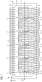
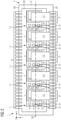
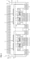
- FIG. 1 to Fig. 5 schematically and exemplarily illustrates a section of a horizontal projection of a power semiconductor device 1, herein also simply referred to as device 1, in accordance with some embodiments.
- the following description refers to each of theses Figures, if not explicitly stated otherwise.
- the power semiconductor device 1 comprises a package 2 having a housing 20, wherein the housing 20 has a first side 201 and a second side 202 opposite to the first side 201.
- the first side 201 and the second side 202 form opposite vertical sidewalls of the housing 20 and extend in parallel to the vertical direction Z and the first lateral direction X.
- the housing 20 may further have a top side and a footprint side, e.g., both extend in parallel to the first lateral direction X and the second lateral direction Y.
- the package 2 may for example have a surface-mounted-device, SMD, configuration, either with top side cooling or with bottom side cooling, or a through-hole-device configuration.
- a plurality of, e.g., identical, power semiconductor chips 1-1 to 1-5 are arranged within the housing 20.
- the Figures show variants with four or five chips, wherein the device 1 may of course comprise more or less than four/five chips.
- each of the power semiconductor chips 1-1 to 1-4/1-5 is identically configured.
- the chips may be identical in terms of size, function and structure.
- each chip has a MOSFET configuration.
- the chip 1-1 may comprise a semiconductor body 10 and, coupled to the semiconductor body 10, a first load terminal 11 and a second load terminal 12.
- the chip 1-1 further comprises a control terminal 13, wherein the semiconductor body 10 is configured to conduct a load current between the first load terminal 11 and the second load terminal 12 based on a control signal received via the control terminal 13.
- Fig. 6 illustrates a vertical design, according to which the first load terminal 11 is arranged at a first side 110 of the semiconductor body 10 and the second load terminal 12 is arranged at a second side 120 of the semiconductor body 10, wherein the first side 110 (e.g., a top side) is opposite of the second side 120 (e.g., a bottom side).
- the semiconductor body 10 extends from the first side 110 along the vertical direction Z to the second side 120.
- the present disclosure is not limited to chips having a vertical design.
- the chips exhibit a horizontal design according to which both load terminals 11 and 12 are arranged at the same side, e.g., either at the first side 110 or at the second side 120.
- the chip 1-1 may further comprise a sense terminal 14, e.g., for sensing a temperature of the chip 1-1 or another parameter.
- the chip 1-1 may have a MOSFET (or another unipolar) configuration and the semiconductor body 10 may be structured, in terms of doped regions, electrodes etc., accordingly.
- the first load terminal 11 may be a source terminal
- the second load terminal 12 may be a drain terminal
- the control terminal 13 may be a gate terminal.
- the chip 1-1 may have an IGBT (or another bipolar) configuration and the semiconductor body 10 may be structured, in terms of doped regions, electrodes etc., accordingly.
- the first load terminal 11 may be an emitter terminal
- the second load terminal 12 may be a collector terminal
- the control terminal 13 may be a gate terminal.
- the semiconductor body 10 of the chip 1-1 can be made of a wide-bandgap-semiconductor material, such as silicon carbide, SiC, or gallium nitride, GaN.
- the chip 1-1 may have a GaN-FET configuration, e.g., a lateral GaN-HEMT (High Electron Mobility Transistor) configuration.
- the semiconductor body 10 is made of silicon, Si.
- the remaining chips 1-2 to 1-4/1-5 of the plurality of chips in the package 2 may be identically configured as chip 1-1.
- the power semiconductor device 1 comprises a plurality of outside terminals 21, 22, 23 configured to provide for an electrical connection between the terminals 11, 12, 13 of the chips 1-1 to 1-2/1-5 within the housing 20 and components of a power circuit (not illustrated) external of the package 2.
- the outside terminals may exhibit a pin structure, as illustrated in Figs. 1 to 5 .
- the part of the respective outside terminal external of the housing 20 may be configured to be coupled to a terminal of circuit, e.g., a converter or inverter circuit, e.g., by soldering.
- the outside terminals comprise:
- Such configuration may allow for an advantageous parallel operation of the chips 1-1 to 1-4/1-5 within the housing 20.
- the chips 1-1 to 1-4/1-5 may be connected in parallel.
- each of the one or more first outside terminals 21 may be electrically connected with each of the first load terminals 11, wherein such parallel connection may occur within the housing or external thereof, as will be explained in more detail below.
- each control terminal 13 is electrically connected with at least one individual third outside terminal of the plurality of third outside terminals 23.
- each chip 1-1 to 1-4/1-5 may be individually connected.
- each chip 1-1 to 1-4/1-5 may receive the same control signal. Due to the individual connection of the control terminals 13, it may be ensured that a distance between a respective one of the third outside terminal 23 to the control terminal 13 of the respective chip is substantially the same for each chip 1-1 to 1-4/1-5, which may in turn ensure that the chips 1-1 to 1-4/1-5 are indeed operated (e.g., switched) simultaneously.
- a symmetric design is proposed according to which each chip 1-1 to 1-4/1-5 of the device 1 may be connected to external components in the same manner. E.g., when the outside terminals 21, 22 and 23 are subjected to given reference voltage values, each of the plurality of identical chips 1-1 to 1-4/1-5 shows the same function due to substantially identical package internal terminal connections.
- the chips 1-1 to 1-4/1-5 are connected in parallel to fulfill the same switching function.
- the power semiconductor device 1 may be a discrete multi-chip power device, e.g., fulfilling the function of one MOSFET or one IGBT.
- each of the second outside terminals 22 is arranged at the second side 202 of the housing 20.
- Each of the first outside terminals 21 and each of the third outside terminals 23 can be arranged at the first side 201.
- the power semiconductor device 1 further comprises a lead frame structure 220 forming both the second outside terminals 22 and, e.g., within the housing, the electrical connection between the second outside terminals 22 and the second load terminals 12 of the chips 1-1 to 1-4/1-5.
- the second load terminals are arranged at the bottom sides 120 of the chips 1-1 to 1-4/1-5, and the bottom sides 120 of the chips 1-1 to 1-4/1-5 are facing to the footprint side of the package 2.
- the lead frame structure 220 may comprise a plate part extending below the chips 1-1 to 1-4/1-5 to establish the electrical connection with the second load terminals 12.
- each of the first outside terminals 21 and, optionally, each of the third outside terminal 23 can be arranged at the first side 201 of the housing 20, i.e., opposite to the second outside terminals 22. Such arrangement may allow for reliably ensuring an electrical insulation between the first outside terminals 21 and the second outside terminal 22.
- the chips 1-1 to 1-4/1-5 are arranged laterally adjacent to each other along a straight line 290.
- the chips 1-1 to 1-4/1-5 may each be arranged in the same orientation, e.g., such that a distance between the control terminal 13 of the respective chip and the associated third outside terminal is substantially the same for each chip 1-1 to 1-4/1-5.
- each chip 1-1 to 1-4/1-5 may be arranged spaced apart from the package sidewall 201 by the same first distance.
- each chip 1-1 to 1-4/1-5 may be arranged spaced apart from the other package sidewall 202 by the same second distance.
- each of the control terminals 13 may be interrogated based on said at least one individual third outside terminal 23.
- two or more individual third outside terminals 23 may be connected in parallel to interrogate the same control terminal 13, but none of the control terminals 13 is electrically connected, within the housing 20, to another one of the control terminals 13.
- the third outside terminals 23 are electrically insulated from each other.
- the chip-associated third outside terminals 23 are each connected to the control terminal 13 of the respective chip by said at least one bond wire 131 (or another electrically conducting component), wherein each bond wire 131 has a length within the range of 90% to 110% of a reference length. Thereby, it may be ensured that a control signal provided at the third outside terminals 23 becomes effective simultaneously for each chip 1-1 to 1-4/1-5.
- each chip 1-1 to 1-4/1-5 further comprises, e.g., at the first side 110 (cf. Fig. 6 ), a sense terminal 14.
- the power semiconductor device 1 may further comprise a plurality of fourth outside terminals 24, wherein each sense terminal 14 is electrically connected with at least one individual fourth outside terminal of the plurality of fourth outside terminals 24.
- an individual parameter e.g., a temperature or voltage
- the fourth outside terminals may also be arranged at the first side 201 of the housing 20, as illustrated in Figs. 1-5 .
- bond wires 141 or the like may be used.
- each chip 1-1 to 1-4/1-5 further comprises, e.g., at the first side 110 (cf. Fig. 6 ), a further terminal 15, e.g., a further sense terminal, which may ( Figs. 3-5 ) or may not (cf. Fig. 1 and 2 ) be connected to an outside terminal 25.
- a further individual parameter e.g., a temperature or voltage
- each first load terminal 11 is electrically connected with at least one individual first outside terminal of the plurality of first outside terminals 21. Since the chip load current must be carried by the respective at least one individual first outside terminal 21, it can be appropriate to associate for than one, e.g., four respective individual first outside terminals 21 with each chip, as illustrated in Fig. 1 . Further, it shall be understood that the chip's first load terminal 11 may comprise single contiguous first load terminal area, as illustrated in Fig. 2 , or exhibit a distributed structure with separate terminal areas 110, as illustrated in Fig. 1 . In the latter case (cf. Fig. 1 ), each terminal area may be coupled to the chip-associated first outside terminal(s) 21 via an individual bridge member 111. In the first case (cf. Fig. 2 ), the first load terminal 11 may be electrically connected with the chip-associated first outside terminal(s) via a larger bridge member 112, e.g., a clip or the like.
- a larger bridge member 112 e.g., a clip
- each first load terminal 11 of a first subset of the plurality of the chips 1-1, 1-2 is electrically connected with at least one individual first outside terminal of the plurality of first outside terminals 21, and each first load terminal 11 of a second subset of the plurality of the chips 1-3, 1-4 is electrically connected with at least one other individual first outside terminal of the plurality of first outside terminals 21.
- the power semiconductor device 1 further comprises a first clip 210-1 forming the electrical connection between the first load terminals 11 of the first subset of the plurality of the chips 1-1, 1-2 and the least one individual first outside terminal 21.
- a second clip 210-2 forms the electrical connection between the first load terminals 11 of the second subset of the plurality of the chips 1-3, 1-4 and the least one other individual first outside terminal 21.
- such configuration of the package allows flexible adaptation of the use of the chips, e.g., according to different power classes. For example, in case of six chips, two phases each having respective three chips may be used for mid power class applications, or six chips may be individually used for low power class applications.
- the embodiment illustrated in Fig. 5 corresponds to the embodiment of Fig. 4 , but further comprises a sense chip 1-99 for sensing the voltage between the first load terminals 11 and the second load terminals 12.
- a sixth outside terminal 26 is provided to electrically contact, via bond wire 261 a first load terminal 11-99 of the sense chip 1-99.
- a second load terminal (not illustrated) of the sense chip 1-99 is electrically connected with the second load terminal of the power semiconductor chips 1-1 to 1-4, e.g., also via the lead frame structure 220.
- a control terminal 13-99 of the sense chip 1-99 is electrically connected with one of the third outside terminals 23 that is not electrically connected to one of the control terminals of the power semiconductor chips 1-1 to 1-4. Thereby, the sense chip 1-99 may be controlled irrespective of the control of the power semiconductor chips 1-1 to 1-4.
- the power semiconductor device 1 further comprises a clip 210, wherein the clip 210 electrically connects each of the first load terminals 11 within the housing 20 with each other and forms the electrical connection between the first load terminals 11 and the first outside terminals 21.
- the first load terminals 11 are electrically connected with each other within the housing 20, and the second load terminals 12 are electrically connected with each other within the housing 20. That is, in this variant, the power semiconductor chips 1-1 to 1-5 are connected in parallel with each other within the housing 20.
- the clip 210 connects three subsets of the first outside terminals 21 to the first load terminals 11. Yet, since each of the power semiconductor chips 1-1 to 1-5 is associated with said at least one individual third outside terminal 23, each of the power semiconductor chips 1-1 to 1-5 may individually controlled.
- a semiconductor region or layer e.g., the semiconductor body 10 and its regions/zones, e.g., regions etc. can be a Si-region or Si-layer or a SiC-region or SiC-layer.
- the semiconductor body 10 and its regions/zones can be made of any semiconductor material suitable for manufacturing a semiconductor device.
- semiconductor materials include, without being limited thereto, elementary semiconductor materials such as silicon (Si) or germanium (Ge), group IV compound semiconductor materials such as silicon carbide (SiC) or silicon germanium (SiGe), binary, ternary or quaternary III-V semiconductor materials such as gallium nitride (GaN), gallium arsenide (GaAs), aluminum gallium nitride (AlGaN) and aluminum indium nitride (AlInN).
- elementary semiconductor materials such as silicon (Si) or germanium (Ge)
- group IV compound semiconductor materials such as silicon carbide (SiC) or silicon germanium (SiGe)
- binary, ternary or quaternary III-V semiconductor materials such as gallium nitride (GaN), gallium arsenide (GaAs), aluminum gallium nitride (AlGaN)
Landscapes
- Lead Frames For Integrated Circuits (AREA)
- Semiconductor Integrated Circuits (AREA)
Priority Applications (2)
| Application Number | Priority Date | Filing Date | Title |
|---|---|---|---|
| EP22158078.0A EP4231345A1 (de) | 2022-02-22 | 2022-02-22 | Leistungshalbleiterbauelement |
| US18/111,242 US20230268255A1 (en) | 2022-02-22 | 2023-02-17 | Power Semiconductor Device |
Applications Claiming Priority (1)
| Application Number | Priority Date | Filing Date | Title |
|---|---|---|---|
| EP22158078.0A EP4231345A1 (de) | 2022-02-22 | 2022-02-22 | Leistungshalbleiterbauelement |
Publications (1)
| Publication Number | Publication Date |
|---|---|
| EP4231345A1 true EP4231345A1 (de) | 2023-08-23 |
Family
ID=80623642
Family Applications (1)
| Application Number | Title | Priority Date | Filing Date |
|---|---|---|---|
| EP22158078.0A Withdrawn EP4231345A1 (de) | 2022-02-22 | 2022-02-22 | Leistungshalbleiterbauelement |
Country Status (2)
| Country | Link |
|---|---|
| US (1) | US20230268255A1 (de) |
| EP (1) | EP4231345A1 (de) |
Citations (5)
| Publication number | Priority date | Publication date | Assignee | Title |
|---|---|---|---|---|
| JPH0590464A (ja) * | 1991-09-27 | 1993-04-09 | Sanyo Electric Co Ltd | 表面実装型半導体装置 |
| US20080122063A1 (en) * | 2006-06-26 | 2008-05-29 | Sanyo Electric Co., Ltd. | Semiconductor device |
| US20110316135A1 (en) * | 2010-06-29 | 2011-12-29 | On Semiconductor Trading, Ltd. | Semiconductor device and method of manufacturing the same |
| US20130264697A1 (en) * | 2012-04-06 | 2013-10-10 | Sumitomo Electric Industries, Ltd. | Semiconductor device |
| US20190304879A1 (en) * | 2018-03-29 | 2019-10-03 | Rohm Co., Ltd. | Semiconductor device and method formanufacturing the same |
Family Cites Families (6)
| Publication number | Priority date | Publication date | Assignee | Title |
|---|---|---|---|---|
| JP5661052B2 (ja) * | 2012-01-18 | 2015-01-28 | 三菱電機株式会社 | パワー半導体モジュールおよびその製造方法 |
| EP4167279A3 (de) * | 2012-09-20 | 2023-09-13 | Rohm Co., Ltd. | Leistungshalbleiter-modul |
| US10802053B2 (en) * | 2016-09-22 | 2020-10-13 | Infineon Technologies Ag | Configuration of integrated current flow sensor |
| JP7567191B2 (ja) * | 2020-03-27 | 2024-10-16 | 富士電機株式会社 | 半導体モジュール |
| US11721616B2 (en) * | 2020-06-04 | 2023-08-08 | Infineon Technologies Austria Ag | Semiconductor package with signal distribution element |
| JP7582147B2 (ja) * | 2021-10-01 | 2024-11-13 | 三菱電機株式会社 | 半導体装置 |
-
2022
- 2022-02-22 EP EP22158078.0A patent/EP4231345A1/de not_active Withdrawn
-
2023
- 2023-02-17 US US18/111,242 patent/US20230268255A1/en active Pending
Patent Citations (5)
| Publication number | Priority date | Publication date | Assignee | Title |
|---|---|---|---|---|
| JPH0590464A (ja) * | 1991-09-27 | 1993-04-09 | Sanyo Electric Co Ltd | 表面実装型半導体装置 |
| US20080122063A1 (en) * | 2006-06-26 | 2008-05-29 | Sanyo Electric Co., Ltd. | Semiconductor device |
| US20110316135A1 (en) * | 2010-06-29 | 2011-12-29 | On Semiconductor Trading, Ltd. | Semiconductor device and method of manufacturing the same |
| US20130264697A1 (en) * | 2012-04-06 | 2013-10-10 | Sumitomo Electric Industries, Ltd. | Semiconductor device |
| US20190304879A1 (en) * | 2018-03-29 | 2019-10-03 | Rohm Co., Ltd. | Semiconductor device and method formanufacturing the same |
Also Published As
| Publication number | Publication date |
|---|---|
| US20230268255A1 (en) | 2023-08-24 |
Similar Documents
| Publication | Publication Date | Title |
|---|---|---|
| US11018109B2 (en) | Power semiconductor module with low gate path inductance | |
| US8461623B2 (en) | Power semiconductor module | |
| US8476885B2 (en) | Monolithic group III-V power converter | |
| US8546937B2 (en) | Semiconductor device | |
| US8472949B2 (en) | Semiconductor assembly | |
| US6249024B1 (en) | Power module with repositioned positive and reduced inductance and capacitance | |
| US10276552B2 (en) | Semiconductor module | |
| CN114078829B (zh) | 一种智能功率模块 | |
| CN113497010A (zh) | 用于电驱动装置的逆变器的半桥模块及逆变器 | |
| US20190237439A1 (en) | Silicon carbide power module | |
| US20190181854A1 (en) | Drive device | |
| EP0987762B1 (de) | Halbleitermodul | |
| CN109768787A (zh) | 半导体装置及其驱动方法 | |
| US11329000B2 (en) | Package for a multi-chip power semiconductor device | |
| US20220102253A1 (en) | Semiconductor package and method of manufacturing a semiconductor package | |
| US20230268255A1 (en) | Power Semiconductor Device | |
| EP3790047B1 (de) | Multi-chip-modul | |
| US20230197581A1 (en) | Power semiconductor module and method of manufacturing the same | |
| US10396774B2 (en) | Intelligent power module operable to be driven by negative gate voltage | |
| CN109600025B (zh) | 可负压栅极驱动的智能功率模块 | |
| US12132122B2 (en) | Single chip power diode and method of producing a single chip power diode | |
| US20240088796A1 (en) | Semiconductor module | |
| US20250318252A1 (en) | Power Semiconductor Device and Method of Producing a Power Semiconductor Device | |
| US20230395582A1 (en) | Semiconductor device | |
| US11398418B2 (en) | Semiconductor module |
Legal Events
| Date | Code | Title | Description |
|---|---|---|---|
| PUAI | Public reference made under article 153(3) epc to a published international application that has entered the european phase |
Free format text: ORIGINAL CODE: 0009012 |
|
| STAA | Information on the status of an ep patent application or granted ep patent |
Free format text: STATUS: THE APPLICATION HAS BEEN PUBLISHED |
|
| AK | Designated contracting states |
Kind code of ref document: A1 Designated state(s): AL AT BE BG CH CY CZ DE DK EE ES FI FR GB GR HR HU IE IS IT LI LT LU LV MC MK MT NL NO PL PT RO RS SE SI SK SM TR |
|
| 18D | Application deemed to be withdrawn |
Effective date: 20240224 |