EP4235635B1 - Structure d'affichage ayant un diélectrique, et dispositif électronique la comprenant - Google Patents
Structure d'affichage ayant un diélectrique, et dispositif électronique la comprenant Download PDFInfo
- Publication number
- EP4235635B1 EP4235635B1 EP22750054.3A EP22750054A EP4235635B1 EP 4235635 B1 EP4235635 B1 EP 4235635B1 EP 22750054 A EP22750054 A EP 22750054A EP 4235635 B1 EP4235635 B1 EP 4235635B1
- Authority
- EP
- European Patent Office
- Prior art keywords
- layer
- edge
- electronic device
- housing
- display
- Prior art date
- Legal status (The legal status is an assumption and is not a legal conclusion. Google has not performed a legal analysis and makes no representation as to the accuracy of the status listed.)
- Active
Links
Images




Classifications
-
- G—PHYSICS
- G09—EDUCATION; CRYPTOGRAPHY; DISPLAY; ADVERTISING; SEALS
- G09F—DISPLAYING; ADVERTISING; SIGNS; LABELS OR NAME-PLATES; SEALS
- G09F9/00—Indicating arrangements for variable information in which the information is built-up on a support by selection or combination of individual elements
- G09F9/30—Indicating arrangements for variable information in which the information is built-up on a support by selection or combination of individual elements in which the desired character or characters are formed by combining individual elements
-
- H—ELECTRICITY
- H01—ELECTRIC ELEMENTS
- H01Q—ANTENNAS, i.e. RADIO AERIALS
- H01Q1/00—Details of, or arrangements associated with, antennas
- H01Q1/12—Supports; Mounting means
- H01Q1/22—Supports; Mounting means by structural association with other equipment or articles
- H01Q1/24—Supports; Mounting means by structural association with other equipment or articles with receiving set
- H01Q1/241—Supports; Mounting means by structural association with other equipment or articles with receiving set used in mobile communications, e.g. GSM
- H01Q1/242—Supports; Mounting means by structural association with other equipment or articles with receiving set used in mobile communications, e.g. GSM specially adapted for hand-held use
- H01Q1/243—Supports; Mounting means by structural association with other equipment or articles with receiving set used in mobile communications, e.g. GSM specially adapted for hand-held use with built-in antennas
-
- H—ELECTRICITY
- H04—ELECTRIC COMMUNICATION TECHNIQUE
- H04M—TELEPHONIC COMMUNICATION
- H04M1/00—Substation equipment, e.g. for use by subscribers
- H04M1/02—Constructional features of telephone sets
- H04M1/0202—Portable telephone sets, e.g. cordless phones, mobile phones or bar type handsets
- H04M1/026—Details of the structure or mounting of specific components
-
- H—ELECTRICITY
- H04—ELECTRIC COMMUNICATION TECHNIQUE
- H04M—TELEPHONIC COMMUNICATION
- H04M1/00—Substation equipment, e.g. for use by subscribers
- H04M1/02—Constructional features of telephone sets
- H04M1/0202—Portable telephone sets, e.g. cordless phones, mobile phones or bar type handsets
- H04M1/026—Details of the structure or mounting of specific components
- H04M1/0266—Details of the structure or mounting of specific components for a display module assembly
- H04M1/0268—Details of the structure or mounting of specific components for a display module assembly including a flexible display panel
-
- H—ELECTRICITY
- H05—ELECTRIC TECHNIQUES NOT OTHERWISE PROVIDED FOR
- H05K—PRINTED CIRCUITS; CASINGS OR CONSTRUCTIONAL DETAILS OF ELECTRIC APPARATUS; MANUFACTURE OF ASSEMBLAGES OF ELECTRICAL COMPONENTS
- H05K5/00—Casings, cabinets or drawers for electric apparatus
- H05K5/0017—Casings, cabinets or drawers for electric apparatus with operator interface units
- H05K5/0018—Casings, cabinets or drawers for electric apparatus with operator interface units having an electronic display
-
- H—ELECTRICITY
- H05—ELECTRIC TECHNIQUES NOT OTHERWISE PROVIDED FOR
- H05K—PRINTED CIRCUITS; CASINGS OR CONSTRUCTIONAL DETAILS OF ELECTRIC APPARATUS; MANUFACTURE OF ASSEMBLAGES OF ELECTRICAL COMPONENTS
- H05K5/00—Casings, cabinets or drawers for electric apparatus
- H05K5/02—Details
- H05K5/0217—Mechanical details of casings
- H05K5/0226—Hinges
-
- H—ELECTRICITY
- H05—ELECTRIC TECHNIQUES NOT OTHERWISE PROVIDED FOR
- H05K—PRINTED CIRCUITS; CASINGS OR CONSTRUCTIONAL DETAILS OF ELECTRIC APPARATUS; MANUFACTURE OF ASSEMBLAGES OF ELECTRICAL COMPONENTS
- H05K5/00—Casings, cabinets or drawers for electric apparatus
- H05K5/02—Details
- H05K5/03—Covers
-
- H—ELECTRICITY
- H04—ELECTRIC COMMUNICATION TECHNIQUE
- H04M—TELEPHONIC COMMUNICATION
- H04M1/00—Substation equipment, e.g. for use by subscribers
- H04M1/02—Constructional features of telephone sets
- H04M1/0202—Portable telephone sets, e.g. cordless phones, mobile phones or bar type handsets
- H04M1/0206—Portable telephones comprising a plurality of mechanically joined movable body parts, e.g. hinged housings
- H04M1/0208—Portable telephones comprising a plurality of mechanically joined movable body parts, e.g. hinged housings characterized by the relative motions of the body parts
- H04M1/0214—Foldable telephones, i.e. with body parts pivoting to an open position around an axis parallel to the plane they define in closed position
- H04M1/0216—Foldable in one direction, i.e. using a one degree of freedom hinge
Definitions
- the electronic device may transmit and/or receive a radio frequency (RF) signal including a voice signal or data (e.g., a message, a photo, a video, a music file, or a game).
- RF radio frequency
- the electronic device feeds to at least a part of a housing of the electronic device and utilizes it as at least one antenna device for communication of the electronic device.
- KR20190052475A relates to a foldable display device comprising: a display panel including a folding region; and a cover unit disposed on the display panel, wherein at least a part of one surface is a curved surface.
- the thickness of the cover unit at a folding axis of the folding region is constant. Therefore, at least a part of the cover unit may be formed as the curved surface, thereby reducing cracks of the cover unit due to an external impact.
- a foldable electronic device using at least a part of a frame or housing as an antenna radiator in an electronic device of an embodiment may include a metal layer for securing the rigidity of a flexible display and protecting a display structure.
- a weight of the electronic device may be reduced by changing a material of the metal layer into a lightweight material.
- the metal layer is formed of this lightweight material
- the corresponding lightweight material may have a high permittivity.
- a layer formed of a material having a high permittivity forms the outermost edge of the display structure, the radiation performance of an antenna adjacent to this layer may be deteriorated.
- An electronic device of various embodiments of the disclosure includes a housing including a first housing forming a first side surface of the electronic device, a second housing forming a second side surface corresponding to the first side surface, and a hinge connecting the first housing and the second housing, and being switchable to a folded or unfolded state about the hinge, a wireless communication circuit disposed inside the housing and transmitting and/or receiving a signal of a specified frequency by feeding to at least a part of the housing, and a display structure coupled to the housing.
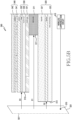
- the display structure of an embodiment includes a cover glass coupled to the housing and forming at least a part of a front surface of the electronic device, a display panel disposed adjacent to one surface of the cover glass, a first layer including a dielectric material and disposed under the display panel, and having a first edge spaced apart from the first side surface by a first distance, and a second layer disposed under the first layer, wherein a second edge of the second layer corresponding to the first edge of the first layer is spaced apart from the first side surface by a second distance less than the first distance.
- An edge of the display panel corresponding to the first edge of the first layer is spaced apart from the first side surface by a third distance greater than the second distance and smaller than the first distance.
- the first edge of the first layer, the second edge of the second layer, and the edge of the display panel are formed in a region corresponding to a region which operates as an antenna radiator by being fed from the wireless communication circuit among the housing.
- the deterioration of antenna performance due to the application of a lightweight material to a metal layer may be improved.
- the damage or deformation of a display structure capable of occurring as a metal layer employs a lightweight material and a structure thereof is changed may be reduced.
- the processor 120 may include a main processor 121 (e.g., a central processing unit (CPU) or an application processor (AP)), or an auxiliary processor 123 (e.g., a graphics processing unit (GPU), a neural processing unit (NPU), an image signal processor (ISP), a sensor hub processor, or a communication processor (CP)) that is operable independently from, or in conjunction with, the main processor 121.
- a main processor 121 e.g., a central processing unit (CPU) or an application processor (AP)
- auxiliary processor 123 e.g., a graphics processing unit (GPU), a neural processing unit (NPU), an image signal processor (ISP), a sensor hub processor, or a communication processor (CP)
- the main processor 121 may be adapted to consume less power than the main processor 121, or to be specific to a specified function.
- the auxiliary processor 123 may be implemented as separate from, or as part of the main processor 121.
- the audio module 170 may convert a sound into an electrical signal and vice versa. According to an embodiment, the audio module 170 may obtain the sound via the input module 150, or output the sound via the sound output module 155 or a headphone of an external electronic device (e.g., an electronic device 102) directly (e.g., wiredly) or wirelessly coupled with the electronic device 101.
- an external electronic device e.g., an electronic device 102
- directly e.g., wiredly
- wirelessly e.g., wirelessly
- the wireless communication module 192 may support various technologies for securing performance on a high-frequency band, such as, e.g., beamforming, massive multiple-input and multiple-output (massive MIMO), full dimensional MIMO (FD-MIMO), array antenna, analog beam-forming, or large scale antenna.
- the wireless communication module 192 may support various requirements specified in the electronic device 101, an external electronic device (e.g., the electronic device 104), or a network system (e.g., the second network 199).
- the wireless communication module 192 may support a peak data rate (e.g., 20Gbps or more) for implementing eMBB, loss coverage (e.g., 164dB or less) for implementing mMTC, or U-plane latency (e.g., 0.5ms or less for each of downlink (DL) and uplink (UL), or a round trip of 1ms or less) for implementing URLLC.
- a peak data rate e.g., 20Gbps or more
- loss coverage e.g., 164dB or less
- U-plane latency e.g., 0.5ms or less for each of downlink (DL) and uplink (UL), or a round trip of 1ms or less
- the signal or the power may then be transmitted or received between the communication module 190 and the external electronic device via the selected at least one antenna.
- another component e.g., a radio frequency integrated circuit (RFIC)
- RFIC radio frequency integrated circuit
- the antenna module 197 may form a mmWave antenna module.
- the mmWave antenna module may include a printed circuit board, a RFIC disposed on a first surface (e.g., the bottom surface) of the printed circuit board, or adjacent to the first surface and capable of supporting a designated high-frequency band (e.g., the mmWave band), and a plurality of antennas (e.g., array antennas) disposed on a second surface (e.g., the top or a side surface) of the printed circuit board, or adjacent to the second surface and capable of transmitting or receiving signals of the designated high-frequency band.
- a RFIC disposed on a first surface (e.g., the bottom surface) of the printed circuit board, or adjacent to the first surface and capable of supporting a designated high-frequency band (e.g., the mmWave band)
- a plurality of antennas e.g., array antennas
- At least some of the above-described components may be coupled mutually and communicate signals (e.g., commands or data) therebetween via an inter-peripheral communication scheme (e.g., a bus, general purpose input and output (GPIO), serial peripheral interface (SPI), or mobile industry processor interface (MIPI)).
- an inter-peripheral communication scheme e.g., a bus, general purpose input and output (GPIO), serial peripheral interface (SPI), or mobile industry processor interface (MIPI)
- commands or data may be transmitted or received between the electronic device 101 and the external electronic device 104 via the server 108 coupled with the second network 199.
- Each of the electronic devices 102 or 104 may be a device of a same type as, or a different type, from the electronic device 101.
- all or some of operations to be executed at the electronic device 101 may be executed at one or more of the external electronic devices 102, 104, or 108. For example, if the electronic device 101 should perform a function or a service automatically, or in response to a request from a user or another device, the electronic device 101, instead of, or in addition to, executing the function or the service, may request the one or more external electronic devices to perform at least part of the function or the service.
- the one or more external electronic devices receiving the request may perform the at least part of the function or the service requested, or an additional function or an additional service related to the request, and transfer an outcome of the performing to the electronic device 101.
- the electronic device 101 may provide the outcome, with or without further processing of the outcome, as at least part of a reply to the request.
- a cloud computing, distributed computing, mobile edge computing (MEC), or client-server computing technology may be used, for example.
- the electronic device 101 may provide ultra low-latency services using, e.g., distributed computing or mobile edge computing.
- the external electronic device 104 may include an internet-of-things (IoT) device.
- the server 108 may be an intelligent server using machine learning and/or a neural network.
- the external electronic device 104 or the server 108 may be included in the second network 199.
- the electronic device 101 may be applied to intelligent services (e.g., smart home, smart city, smart car, or healthcare) based on 5G communication technology or IoT-related technology.
- the electronic device may be one of various types of electronic devices.
- the electronic devices may include, for example, a portable communication device (e.g., a smartphone), a computer device, a portable multimedia device, a portable medical device, a camera, a wearable device, or a home appliance. According to an embodiment of the disclosure, the electronic devices are not limited to those described above.
- each of such phrases as “A or B,” “at least one of A and B,” “at least one of A or B,” “A, B, or C,” “at least one of A, B, and C,” and “at least one of A, B, or C,” may include any one of, or all possible combinations of the items enumerated together in a corresponding one of the phrases.
- such terms as “1st” and “2nd,” or “first” and “second” may be used to simply distinguish a corresponding component from another, and does not limit the components in other aspect (e.g., importance or order).
- an element e.g., a first element
- the element may be coupled with the other element directly (e.g., wiredly), wirelessly, or via a third element.
- module may include a unit implemented in hardware, software, or firmware, and may interchangeably be used with other terms, for example, "logic,” “logic block,” “part,” or “circuitry”.
- a module may be a single integral component, or a minimum unit or part thereof, adapted to perform one or more functions.
- the module may be implemented in a form of an application-specific integrated circuit (ASIC).
- ASIC application-specific integrated circuit
- Various embodiments as set forth herein may be implemented as software (e.g., the program 140) including one or more instructions that are stored in a storage medium (e.g., internal memory 136 or external memory 138) that is readable by a machine (e.g., the electronic device 101).
- a processor e.g., the processor 120 of the machine (e.g., the electronic device 101) may invoke at least one of the one or more instructions stored in the storage medium, and execute it, with or without using one or more other components under the control of the processor. This allows the machine to be operated to perform at least one function according to the at least one instruction invoked.
- the one or more instructions may include a code generated by a complier or a code executable by an interpreter.
- the machine-readable storage medium may be provided in the form of a non-transitory storage medium.
- non-transitory simply means that the storage medium is a tangible device, and does not include a signal (e.g., an electromagnetic wave), but this term does not differentiate between where data is semi-permanently stored in the storage medium and where the data is temporarily stored in the storage medium.
- a signal e.g., an electromagnetic wave
- a method may be included and provided in a computer program product.
- the computer program product may be traded as a product between a seller and a buyer.
- the computer program product may be distributed in the form of a machine-readable storage medium (e.g., compact disc read only memory (CD-ROM)), or be distributed (e.g., downloaded or uploaded) online via an application store (e.g., PlayStore TM ), or between two user devices (e.g., smart phones) directly. If distributed online, at least part of the computer program product may be temporarily generated or at least temporarily stored in the machine-readable storage medium, such as memory of the manufacturer's server, a server of the application store, or a relay server.
- CD-ROM compact disc read only memory
- an application store e.g., PlayStore TM
- two user devices e.g., smart phones
- each component e.g., a module or a program of the above-described components may include a single entity or multiple entities, and some of the multiple entities may be separately disposed in different components. According to various embodiments, one or more of the above-described components may be omitted, or one or more other components may be added. Alternatively or additionally, a plurality of components (e.g., modules or programs) may be integrated into a single component. In such a case, according to various embodiments, the integrated component may still perform one or more functions of each of the plurality of components in the same or similar manner as they are performed by a corresponding one of the plurality of components before the integration.
- operations performed by the module, the program, or another component may be carried out sequentially, in parallel, repeatedly, or heuristically, or one or more of the operations may be executed in a different order or omitted, or one or more other operations may be added.
- FIG. 2A illustrates an electronic device of an unfolded state according to an embodiment.
- FIG. 2B illustrates an electronic device of a folded state according to an embodiment.
- the electronic device 101 may include a foldable housing 200 (hereinafter, abbreviated as “housing” 200) and a flexible or foldable display 260 (hereinafter, abbreviated as “display” 260) which is disposed in a space formed by the housing 200.
- a surface on which the display 260 is disposed may be referred to as a first surface, or a front surface of the electronic device 101.
- a surface opposite to the front surface may be referred to as a second surface, or a rear surface of the electronic device 101.
- a surface surrounding a space between the front surface and the rear surface may be referred to as a third surface, or a side surface of the electronic device 101.
- the housing 200 may have a substantially rectangular shape in the unfolded state of FIG. 2A .
- the housing 200 may have a specified width (W1) and a specified length (L1) longer than the specified width (W1).
- the housing 200 may have a specified width (W1) and a specified length (L1) that is substantially equal to or shorter than the specified width (W1).
- the specified width (W1) may be a width of the display 260.
- the housing 200 of the electronic device 101 can be folded or unfolded with a criterion of a folding axis (A) which is substantially in parallel to a long edge of the rectangle (e.g., an edge going in a y-axis direction among edges of the housing 200 of the electronic device 101 in FIG. 2A ).
- A folding axis
- the housing 200 may include a first housing 201, a second housing 202, and a connecting part 203.
- the connecting part 203 may be disposed between the first housing 201 and the second housing 202.
- the connecting part 203 may be coupled to the first housing 201 and the second housing 202, and the first housing 201 and/or the second housing 202 may be rotated centering on the connecting part 203 (or the folding axis (A)).
- the first housing 201 may include a first side member 2011 and a first rear cover 2013.
- the second housing 202 may include a second side member 2021 and a second rear cover 2023.
- the first side member 2011 may extend along an edge of the first housing 201, and may form at least one portion of a side surface of the electronic device 101.
- the first side member 2011 may include at least one conductive portion formed of a conductive material (e.g., a metal).
- the conductive portion may operate as an antenna radiator for transmitting and/or receiving an RF signal.
- the second side member 2021 may form one portion of a side surface of the electronic device 101, and at least one portion of the second side member 2021 may be formed of a conductive material and operate as an antenna radiator.
- an angle or distance between the first side member 2011 and the second side member 2021 may be varied depending on whether the electronic device 101 is in an unfolded state, a folded state, or an intermediate state.
Landscapes
- Engineering & Computer Science (AREA)
- Microelectronics & Electronic Packaging (AREA)
- Signal Processing (AREA)
- Computer Networks & Wireless Communication (AREA)
- Physics & Mathematics (AREA)
- General Physics & Mathematics (AREA)
- Theoretical Computer Science (AREA)
- Telephone Set Structure (AREA)
- Details Of Aerials (AREA)
Claims (9)
- Dispositif électronique (101) comprenant :un boîtier (200) comprenant un premier boîtier (201) formant une première surface latérale (501) du dispositif électronique (101), un second boîtier (202) formant une seconde surface latérale correspondant à la première surface latérale (501), et une charnière (203) reliant le premier boîtier (201) et le second boîtier (202), et pouvant passer à un état plié ou déplié autour de la structure de charnière (203) ;un circuit de communication sans fil (410) disposé à l'intérieur du boîtier et émettant et/ou recevant un signal d'une fréquence spécifiée en alimentant au moins une partie du boîtier (200) ; etune structure d'affichage (260) couplée au boîtier (200),ladite structure d'affichage (260) comprenant :un verre de couverture (340) couplé au boîtier (200) et formant au moins une partie d'une surface avant du dispositif électronique (101) ;un panneau d'affichage (330) disposé adjacent à une surface du verre de couverture (340) ;une première couche (311) comprenant un matériau diélectrique et disposée sous le panneau d'affichage (330), un premier bord (401A, 401B, 511) de la première couche (311) étant espacé de la première surface latérale (501) d'une première distance ; etune seconde couche (320) disposée sous la première couche (311), un second bord (512) de la seconde couche (320) correspondant au premier bord de la première couche (311) étant espacé de la première surface latérale (501) d'une deuxième distance inférieure à la première distance, etun bord (513) du panneau d'affichage (330) correspondant au premier bord de la première couche (311) étant espacé de la première surface latérale (501) d'une troisième distance supérieure à la deuxième distance et inférieure à la première distance,ledit premier bord (401A, 401B, 511) de la première couche (311), ledit second bord (512) de la seconde couche (320) et ledit bord (513) du panneau d'affichage (330) étant formés dans une zone correspondant à une zone qui fonctionne en tant que radiateur d'antenne en étant alimenté à partir du circuit de communication sans fil (410) parmi le boîtier (200).
- Dispositif électronique (101) de la revendication 1, ledit second bord (512) et ledit bord (513) du panneau d'affichage (330) étant disposés entre le premier bord (401A, 401B, 511) et la première surface latérale (501), lorsqu'ils sont vus depuis une direction perpendiculaire à une surface avant du dispositif électronique (101).
- Dispositif électronique (101) de la revendication 1, ladite seconde couche (320) comprenant au moins l'un d'un numériseur (321) ou d'une plaque métallique (322).
- Dispositif électronique (101) de la revendication 1, ladite première couche (311) comprenant un plastique renforcé de fibres de carbone, CFRP.
- Dispositif électronique (101) de la revendication 1, ladite première couche (311) comprenant en outre une couche diélectrique (620) s'étendant à partir du premier bord (401A, 401B, 511), et ladite couche diélectrique (620) comportant une permittivité inférieure ou égale à 6.
- Dispositif électronique (101) de la revendication 1, ledit matériau diélectrique comportant une permittivité supérieur ou égale à 150.
- Dispositif électronique (101) de la revendication 1, ledit premier bord (401A, 401B, 511) de la première couche (311), ledit second bord (512) de la seconde couche (320) et ledit bord (513) du panneau d'affichage (330) étant formés dans une zone espacée d'une distance prédéfinie de la charnière (203).
- Dispositif électronique (101) de la revendication 1, comprenant une couche adhésive (381) disposée entre le panneau d'affichage (330) et la première couche (311),
ladite couche adhésive (381) comportant un bord correspondant au premier bord (401A, 401B, 511) de la première couche (311). - Dispositif électronique (101) de la revendication 1, ladite première couche (311) comprenant un motif de réseau (370) dans au moins une partie de celle-ci.
Applications Claiming Priority (3)
| Application Number | Priority Date | Filing Date | Title |
|---|---|---|---|
| KR20210016877 | 2021-02-05 | ||
| KR1020210058047A KR20220113226A (ko) | 2021-02-05 | 2021-05-04 | 유전체를 포함하는 디스플레이 구조 및 이를 포함하는 전자 장치 |
| PCT/KR2022/001768 WO2022169305A1 (fr) | 2021-02-05 | 2022-02-04 | Structure d'affichage ayant un diélectrique, et dispositif électronique la comprenant |
Publications (3)
| Publication Number | Publication Date |
|---|---|
| EP4235635A1 EP4235635A1 (fr) | 2023-08-30 |
| EP4235635A4 EP4235635A4 (fr) | 2024-05-29 |
| EP4235635B1 true EP4235635B1 (fr) | 2025-04-02 |
Family
ID=82742436
Family Applications (1)
| Application Number | Title | Priority Date | Filing Date |
|---|---|---|---|
| EP22750054.3A Active EP4235635B1 (fr) | 2021-02-05 | 2022-02-04 | Structure d'affichage ayant un diélectrique, et dispositif électronique la comprenant |
Country Status (4)
| Country | Link |
|---|---|
| US (1) | US12322858B2 (fr) |
| EP (1) | EP4235635B1 (fr) |
| JP (1) | JP7850729B2 (fr) |
| WO (1) | WO2022169305A1 (fr) |
Families Citing this family (3)
| Publication number | Priority date | Publication date | Assignee | Title |
|---|---|---|---|---|
| JP7644836B2 (ja) * | 2021-03-05 | 2025-03-12 | サムスン エレクトロニクス カンパニー リミテッド | 誘電層を含むディスプレイ構造を有する電子装置 |
| KR20230116972A (ko) * | 2022-01-28 | 2023-08-07 | 삼성디스플레이 주식회사 | 폴더블 표시 장치 |
| KR20240128746A (ko) * | 2023-02-17 | 2024-08-27 | 삼성디스플레이 주식회사 | 디지타이저 및 이를 포함하는 표시 장치 |
Family Cites Families (25)
| Publication number | Priority date | Publication date | Assignee | Title |
|---|---|---|---|---|
| US5936613A (en) * | 1993-11-05 | 1999-08-10 | Intertactile Technologies Corporation | Rotary circuit control devices with changeable graphics |
| US9477306B1 (en) * | 2010-08-24 | 2016-10-25 | Amazon Technologies, Inc. | Mutamorphic haptic substrate |
| US20140355194A1 (en) | 2012-01-16 | 2014-12-04 | Nec Casio Mobile Communications, Ltd. | Portable terminal device |
| US9134763B2 (en) * | 2013-11-11 | 2015-09-15 | Symbol Technologies, Llc | Externally mounted display device |
| TWI545381B (zh) * | 2014-05-21 | 2016-08-11 | 群創光電股份有限公司 | 顯示裝置 |
| TWI575756B (zh) * | 2015-01-13 | 2017-03-21 | 群創光電股份有限公司 | 顯示面板 |
| CN110137213B (zh) * | 2018-02-09 | 2025-03-25 | 京东方科技集团股份有限公司 | 像素排列结构及其显示方法、显示基板 |
| TWI616025B (zh) * | 2016-06-16 | 2018-02-21 | 和碩聯合科技股份有限公司 | 穿戴式電子裝置 |
| EP3557852A4 (fr) * | 2016-12-16 | 2020-07-29 | LG Electronics Inc. -1- | Terminal mobile |
| KR101834793B1 (ko) * | 2017-07-28 | 2018-03-06 | 엘지디스플레이 주식회사 | 플렉서블 디스플레이 및 이를 포함하는 전자 장치 |
| KR102408410B1 (ko) * | 2017-11-08 | 2022-06-10 | 엘지디스플레이 주식회사 | 폴더블 표시 장치 |
| CN111479907A (zh) * | 2017-12-19 | 2020-07-31 | 埃克森美孚研究工程公司 | 低硫船用燃料组合物 |
| JP6491770B2 (ja) * | 2018-02-27 | 2019-03-27 | レノボ・シンガポール・プライベート・リミテッド | 携帯用情報機器 |
| CN110290235B (zh) * | 2018-03-19 | 2022-11-18 | 华为技术有限公司 | 电子设备 |
| KR102540815B1 (ko) * | 2018-06-01 | 2023-06-08 | 삼성전자주식회사 | 폴더블 디스플레이를 포함하는 전자 장치 |
| KR102637071B1 (ko) | 2018-11-16 | 2024-02-16 | 삼성디스플레이 주식회사 | 표시장치 및 이를 갖는 전자장치 |
| CN111384585B (zh) * | 2018-12-29 | 2021-08-31 | Oppo广东移动通信有限公司 | 电子设备及电子设备的控制方法 |
| KR102563626B1 (ko) | 2019-01-09 | 2023-08-04 | 삼성전자 주식회사 | 플렉서블 디스플레이 및 이를 포함하는 전자장치 |
| KR102613522B1 (ko) | 2019-02-18 | 2023-12-13 | 삼성전자주식회사 | 베젤 처짐 방지 구조를 포함하는 폴더블 전자 장치 |
| JP2020201698A (ja) * | 2019-06-10 | 2020-12-17 | レノボ・シンガポール・プライベート・リミテッド | 携帯用情報機器及びディスプレイアセンブリ |
| WO2020248246A1 (fr) * | 2019-06-14 | 2020-12-17 | 京东方科技集团股份有限公司 | Substrat d'affichage et son procédé de fabrication et appareil d'affichage |
| KR102121267B1 (ko) | 2019-06-25 | 2020-06-10 | 삼성전자주식회사 | 플렉서블 디스플레이 소자를 구비한 접철식 전자 기기 |
| KR102682163B1 (ko) | 2019-07-05 | 2024-07-08 | 삼성전자주식회사 | 안테나 구조체 및 그를 포함하는 전자 장치 |
| KR102221470B1 (ko) * | 2019-08-08 | 2021-03-02 | 엘지전자 주식회사 | 디스플레이 장치의 제조방법 및 디스플레이 장치 제조를 위한 기판 |
| US20220399375A1 (en) * | 2020-12-23 | 2022-12-15 | Chengdu Boe Optoelectronics Technology Co., Ltd. | Display panel and fabrication method thereof |
-
2022
- 2022-02-04 EP EP22750054.3A patent/EP4235635B1/fr active Active
- 2022-02-04 WO PCT/KR2022/001768 patent/WO2022169305A1/fr not_active Ceased
- 2022-02-04 JP JP2023541650A patent/JP7850729B2/ja active Active
- 2022-08-23 US US17/893,821 patent/US12322858B2/en active Active
Also Published As
| Publication number | Publication date |
|---|---|
| JP2024505814A (ja) | 2024-02-08 |
| WO2022169305A1 (fr) | 2022-08-11 |
| JP7850729B2 (ja) | 2026-04-23 |
| EP4235635A1 (fr) | 2023-08-30 |
| US12322858B2 (en) | 2025-06-03 |
| EP4235635A4 (fr) | 2024-05-29 |
| US20220407219A1 (en) | 2022-12-22 |
Similar Documents
| Publication | Publication Date | Title |
|---|---|---|
| US11995305B2 (en) | Predictive presentation of a user interface on an extendible display | |
| US12322858B2 (en) | Display structure including dielectric material and electronic device including same | |
| US12028999B2 (en) | Electronic device including display | |
| EP4321963B1 (fr) | Dispositif électronique pliable comprenant une pluralité de capteurs d'empreintes digitales | |
| US12453253B2 (en) | Electronic device including camera module | |
| KR20220113226A (ko) | 유전체를 포함하는 디스플레이 구조 및 이를 포함하는 전자 장치 | |
| US12493319B2 (en) | Display structure including dielectric and electronic device including same | |
| US12394886B2 (en) | Display structure including dielectric layer and electronic device including same | |
| US12496799B2 (en) | Electronic device including foldable display | |
| US20230341965A1 (en) | Electronic device including touch sensor integrated display | |
| US20220182521A1 (en) | Electronic device including flexible display and camera | |
| RU2825009C1 (ru) | Электронное устройство, включающее в себя конструкцию дисплея (варианты) | |
| US12443240B2 (en) | Electronic device comprising sensor panel | |
| US12560979B2 (en) | Electronic device including foldable display | |
| EP4472181A1 (fr) | Dispositif électronique comprenant une structure pour supporter une carte de circuit imprimé souple | |
| EP4583497A1 (fr) | Affichage de fourniture de région d'affichage uniforme et dispositif électronique le comprenant | |
| EP4641358A1 (fr) | Dispositif électronique comprenant une structure pour réduire les dommages à un écran | |
| US20240370060A1 (en) | Window glass and electronic device including same | |
| EP4629038A1 (fr) | Module d'affichage comprenant une structure destinée à réduire les dommages, et dispositif électronique le comprenant | |
| US20260072476A1 (en) | Electronic device including reinforcement member | |
| EP4546562A1 (fr) | Structure d'antenne et dispositif électronique la comprenant | |
| KR20220125657A (ko) | 유전층을 포함하는 디스플레이 구조 및 이를 포함하는 전자 장치 | |
| KR20220125667A (ko) | 유전층을 포함하는 디스플레이 구조 및 이를 포함하는 전자 장치 | |
| CN116917837A (zh) | 包括介电层的显示器结构和包括该显示器结构的电子装置 | |
| KR20230055319A (ko) | 폴더블 디스플레이를 포함하는 전자 장치 |
Legal Events
| Date | Code | Title | Description |
|---|---|---|---|
| STAA | Information on the status of an ep patent application or granted ep patent |
Free format text: STATUS: THE INTERNATIONAL PUBLICATION HAS BEEN MADE |
|
| PUAI | Public reference made under article 153(3) epc to a published international application that has entered the european phase |
Free format text: ORIGINAL CODE: 0009012 |
|
| STAA | Information on the status of an ep patent application or granted ep patent |
Free format text: STATUS: REQUEST FOR EXAMINATION WAS MADE |
|
| 17P | Request for examination filed |
Effective date: 20230526 |
|
| AK | Designated contracting states |
Kind code of ref document: A1 Designated state(s): AL AT BE BG CH CY CZ DE DK EE ES FI FR GB GR HR HU IE IS IT LI LT LU LV MC MK MT NL NO PL PT RO RS SE SI SK SM TR |
|
| DAV | Request for validation of the european patent (deleted) | ||
| DAX | Request for extension of the european patent (deleted) | ||
| A4 | Supplementary search report drawn up and despatched |
Effective date: 20240430 |
|
| RIC1 | Information provided on ipc code assigned before grant |
Ipc: H01Q 1/24 20060101ALI20240424BHEP Ipc: H04M 1/02 20060101ALI20240424BHEP Ipc: G09F 9/30 20060101AFI20240424BHEP |
|
| GRAP | Despatch of communication of intention to grant a patent |
Free format text: ORIGINAL CODE: EPIDOSNIGR1 |
|
| STAA | Information on the status of an ep patent application or granted ep patent |
Free format text: STATUS: GRANT OF PATENT IS INTENDED |
|
| RIC1 | Information provided on ipc code assigned before grant |
Ipc: H01Q 1/24 20060101ALI20240930BHEP Ipc: H04M 1/02 20060101ALI20240930BHEP Ipc: G09F 9/30 20060101AFI20240930BHEP |
|
| INTG | Intention to grant announced |
Effective date: 20241014 |
|
| GRAS | Grant fee paid |
Free format text: ORIGINAL CODE: EPIDOSNIGR3 |
|
| GRAA | (expected) grant |
Free format text: ORIGINAL CODE: 0009210 |
|
| STAA | Information on the status of an ep patent application or granted ep patent |
Free format text: STATUS: THE PATENT HAS BEEN GRANTED |
|
| AK | Designated contracting states |
Kind code of ref document: B1 Designated state(s): AL AT BE BG CH CY CZ DE DK EE ES FI FR GB GR HR HU IE IS IT LI LT LU LV MC MK MT NL NO PL PT RO RS SE SI SK SM TR |
|
| REG | Reference to a national code |
Ref country code: GB Ref legal event code: FG4D |
|
| REG | Reference to a national code |
Ref country code: CH Ref legal event code: EP |
|
| REG | Reference to a national code |
Ref country code: DE Ref legal event code: R096 Ref document number: 602022012664 Country of ref document: DE |
|
| REG | Reference to a national code |
Ref country code: IE Ref legal event code: FG4D |
|
| REG | Reference to a national code |
Ref country code: NL Ref legal event code: MP Effective date: 20250402 |
|
| PG25 | Lapsed in a contracting state [announced via postgrant information from national office to epo] |
Ref country code: NL Free format text: LAPSE BECAUSE OF FAILURE TO SUBMIT A TRANSLATION OF THE DESCRIPTION OR TO PAY THE FEE WITHIN THE PRESCRIBED TIME-LIMIT Effective date: 20250402 |
|
| REG | Reference to a national code |
Ref country code: AT Ref legal event code: MK05 Ref document number: 1782098 Country of ref document: AT Kind code of ref document: T Effective date: 20250402 |
|
| PG25 | Lapsed in a contracting state [announced via postgrant information from national office to epo] |
Ref country code: FI Free format text: LAPSE BECAUSE OF FAILURE TO SUBMIT A TRANSLATION OF THE DESCRIPTION OR TO PAY THE FEE WITHIN THE PRESCRIBED TIME-LIMIT Effective date: 20250402 Ref country code: ES Free format text: LAPSE BECAUSE OF FAILURE TO SUBMIT A TRANSLATION OF THE DESCRIPTION OR TO PAY THE FEE WITHIN THE PRESCRIBED TIME-LIMIT Effective date: 20250402 Ref country code: PT Free format text: LAPSE BECAUSE OF FAILURE TO SUBMIT A TRANSLATION OF THE DESCRIPTION OR TO PAY THE FEE WITHIN THE PRESCRIBED TIME-LIMIT Effective date: 20250804 |
|
| REG | Reference to a national code |
Ref country code: LT Ref legal event code: MG9D |
|
| PG25 | Lapsed in a contracting state [announced via postgrant information from national office to epo] |
Ref country code: NO Free format text: LAPSE BECAUSE OF FAILURE TO SUBMIT A TRANSLATION OF THE DESCRIPTION OR TO PAY THE FEE WITHIN THE PRESCRIBED TIME-LIMIT Effective date: 20250702 Ref country code: GR Free format text: LAPSE BECAUSE OF FAILURE TO SUBMIT A TRANSLATION OF THE DESCRIPTION OR TO PAY THE FEE WITHIN THE PRESCRIBED TIME-LIMIT Effective date: 20250703 |
|
| PG25 | Lapsed in a contracting state [announced via postgrant information from national office to epo] |
Ref country code: PL Free format text: LAPSE BECAUSE OF FAILURE TO SUBMIT A TRANSLATION OF THE DESCRIPTION OR TO PAY THE FEE WITHIN THE PRESCRIBED TIME-LIMIT Effective date: 20250402 |
|
| PG25 | Lapsed in a contracting state [announced via postgrant information from national office to epo] |
Ref country code: BG Free format text: LAPSE BECAUSE OF FAILURE TO SUBMIT A TRANSLATION OF THE DESCRIPTION OR TO PAY THE FEE WITHIN THE PRESCRIBED TIME-LIMIT Effective date: 20250402 |
|
| PG25 | Lapsed in a contracting state [announced via postgrant information from national office to epo] |
Ref country code: HR Free format text: LAPSE BECAUSE OF FAILURE TO SUBMIT A TRANSLATION OF THE DESCRIPTION OR TO PAY THE FEE WITHIN THE PRESCRIBED TIME-LIMIT Effective date: 20250402 |
|
| PG25 | Lapsed in a contracting state [announced via postgrant information from national office to epo] |
Ref country code: AT Free format text: LAPSE BECAUSE OF FAILURE TO SUBMIT A TRANSLATION OF THE DESCRIPTION OR TO PAY THE FEE WITHIN THE PRESCRIBED TIME-LIMIT Effective date: 20250402 |
|
| PG25 | Lapsed in a contracting state [announced via postgrant information from national office to epo] |
Ref country code: RS Free format text: LAPSE BECAUSE OF FAILURE TO SUBMIT A TRANSLATION OF THE DESCRIPTION OR TO PAY THE FEE WITHIN THE PRESCRIBED TIME-LIMIT Effective date: 20250702 |
|
| PG25 | Lapsed in a contracting state [announced via postgrant information from national office to epo] |
Ref country code: IS Free format text: LAPSE BECAUSE OF FAILURE TO SUBMIT A TRANSLATION OF THE DESCRIPTION OR TO PAY THE FEE WITHIN THE PRESCRIBED TIME-LIMIT Effective date: 20250802 |
|
| PG25 | Lapsed in a contracting state [announced via postgrant information from national office to epo] |
Ref country code: LV Free format text: LAPSE BECAUSE OF FAILURE TO SUBMIT A TRANSLATION OF THE DESCRIPTION OR TO PAY THE FEE WITHIN THE PRESCRIBED TIME-LIMIT Effective date: 20250402 |
|
| REG | Reference to a national code |
Ref country code: DE Ref legal event code: R097 Ref document number: 602022012664 Country of ref document: DE |
|
| PG25 | Lapsed in a contracting state [announced via postgrant information from national office to epo] |
Ref country code: SM Free format text: LAPSE BECAUSE OF FAILURE TO SUBMIT A TRANSLATION OF THE DESCRIPTION OR TO PAY THE FEE WITHIN THE PRESCRIBED TIME-LIMIT Effective date: 20250402 Ref country code: DK Free format text: LAPSE BECAUSE OF FAILURE TO SUBMIT A TRANSLATION OF THE DESCRIPTION OR TO PAY THE FEE WITHIN THE PRESCRIBED TIME-LIMIT Effective date: 20250402 |
|
| PG25 | Lapsed in a contracting state [announced via postgrant information from national office to epo] |
Ref country code: CZ Free format text: LAPSE BECAUSE OF FAILURE TO SUBMIT A TRANSLATION OF THE DESCRIPTION OR TO PAY THE FEE WITHIN THE PRESCRIBED TIME-LIMIT Effective date: 20250402 |
|
| PG25 | Lapsed in a contracting state [announced via postgrant information from national office to epo] |
Ref country code: EE Free format text: LAPSE BECAUSE OF FAILURE TO SUBMIT A TRANSLATION OF THE DESCRIPTION OR TO PAY THE FEE WITHIN THE PRESCRIBED TIME-LIMIT Effective date: 20250402 |
|
| PG25 | Lapsed in a contracting state [announced via postgrant information from national office to epo] |
Ref country code: SK Free format text: LAPSE BECAUSE OF FAILURE TO SUBMIT A TRANSLATION OF THE DESCRIPTION OR TO PAY THE FEE WITHIN THE PRESCRIBED TIME-LIMIT Effective date: 20250402 |
|
| PG25 | Lapsed in a contracting state [announced via postgrant information from national office to epo] |
Ref country code: IT Free format text: LAPSE BECAUSE OF FAILURE TO SUBMIT A TRANSLATION OF THE DESCRIPTION OR TO PAY THE FEE WITHIN THE PRESCRIBED TIME-LIMIT Effective date: 20250402 |
|
| PLBE | No opposition filed within time limit |
Free format text: ORIGINAL CODE: 0009261 |
|
| STAA | Information on the status of an ep patent application or granted ep patent |
Free format text: STATUS: NO OPPOSITION FILED WITHIN TIME LIMIT |
|
| REG | Reference to a national code |
Ref country code: CH Ref legal event code: L10 Free format text: ST27 STATUS EVENT CODE: U-0-0-L10-L00 (AS PROVIDED BY THE NATIONAL OFFICE) Effective date: 20260211 |
|
| 26N | No opposition filed |
Effective date: 20260105 |
|
| PGFP | Annual fee paid to national office [announced via postgrant information from national office to epo] |
Ref country code: DE Payment date: 20260120 Year of fee payment: 5 |