EP4235744A2 - Dispositif d'optimisation/collimateur de flux pouvant être polarisé pour chambre de pulvérisation pvd - Google Patents
Dispositif d'optimisation/collimateur de flux pouvant être polarisé pour chambre de pulvérisation pvd Download PDFInfo
- Publication number
- EP4235744A2 EP4235744A2 EP23175161.1A EP23175161A EP4235744A2 EP 4235744 A2 EP4235744 A2 EP 4235744A2 EP 23175161 A EP23175161 A EP 23175161A EP 4235744 A2 EP4235744 A2 EP 4235744A2
- Authority
- EP
- European Patent Office
- Prior art keywords
- collimator
- apertures
- aspect ratio
- region
- collimator assembly
- Prior art date
- Legal status (The legal status is an assumption and is not a legal conclusion. Google has not performed a legal analysis and makes no representation as to the accuracy of the status listed.)
- Pending
Links
Images



Classifications
-
- H—ELECTRICITY
- H01—ELECTRIC ELEMENTS
- H01J—ELECTRIC DISCHARGE TUBES OR DISCHARGE LAMPS
- H01J37/00—Discharge tubes with provision for introducing objects or material to be exposed to the discharge, e.g. for the purpose of examination or processing thereof
- H01J37/32—Gas-filled discharge tubes
- H01J37/34—Gas-filled discharge tubes operating with cathodic sputtering
- H01J37/3411—Constructional aspects of the reactor
- H01J37/3447—Collimators, shutters, apertures
-
- C—CHEMISTRY; METALLURGY
- C23—COATING METALLIC MATERIAL; COATING MATERIAL WITH METALLIC MATERIAL; CHEMICAL SURFACE TREATMENT; DIFFUSION TREATMENT OF METALLIC MATERIAL; COATING BY VACUUM EVAPORATION, BY SPUTTERING, BY ION IMPLANTATION OR BY CHEMICAL VAPOUR DEPOSITION, IN GENERAL; INHIBITING CORROSION OF METALLIC MATERIAL OR INCRUSTATION IN GENERAL
- C23C—COATING METALLIC MATERIAL; COATING MATERIAL WITH METALLIC MATERIAL; SURFACE TREATMENT OF METALLIC MATERIAL BY DIFFUSION INTO THE SURFACE, BY CHEMICAL CONVERSION OR SUBSTITUTION; COATING BY VACUUM EVAPORATION, BY SPUTTERING, BY ION IMPLANTATION OR BY CHEMICAL VAPOUR DEPOSITION, IN GENERAL
- C23C14/00—Coating by vacuum evaporation, by sputtering or by ion implantation of the coating forming material
- C23C14/22—Coating by vacuum evaporation, by sputtering or by ion implantation of the coating forming material characterised by the process of coating
- C23C14/34—Sputtering
- C23C14/3407—Cathode assembly for sputtering apparatus, e.g. Target
-
- H—ELECTRICITY
- H10—SEMICONDUCTOR DEVICES; ELECTRIC SOLID-STATE DEVICES NOT OTHERWISE PROVIDED FOR
- H10P—GENERIC PROCESSES OR APPARATUS FOR THE MANUFACTURE OR TREATMENT OF DEVICES COVERED BY CLASS H10
- H10P14/00—Formation of materials, e.g. in the shape of layers or pillars
- H10P14/40—Formation of materials, e.g. in the shape of layers or pillars of conductive or resistive materials
- H10P14/42—Formation of materials, e.g. in the shape of layers or pillars of conductive or resistive materials using a gas or vapour
- H10P14/44—Physical vapour deposition [PVD]
-
- C—CHEMISTRY; METALLURGY
- C23—COATING METALLIC MATERIAL; COATING MATERIAL WITH METALLIC MATERIAL; CHEMICAL SURFACE TREATMENT; DIFFUSION TREATMENT OF METALLIC MATERIAL; COATING BY VACUUM EVAPORATION, BY SPUTTERING, BY ION IMPLANTATION OR BY CHEMICAL VAPOUR DEPOSITION, IN GENERAL; INHIBITING CORROSION OF METALLIC MATERIAL OR INCRUSTATION IN GENERAL
- C23C—COATING METALLIC MATERIAL; COATING MATERIAL WITH METALLIC MATERIAL; SURFACE TREATMENT OF METALLIC MATERIAL BY DIFFUSION INTO THE SURFACE, BY CHEMICAL CONVERSION OR SUBSTITUTION; COATING BY VACUUM EVAPORATION, BY SPUTTERING, BY ION IMPLANTATION OR BY CHEMICAL VAPOUR DEPOSITION, IN GENERAL
- C23C14/00—Coating by vacuum evaporation, by sputtering or by ion implantation of the coating forming material
- C23C14/04—Coating on selected surface areas, e.g. using masks
- C23C14/046—Coating cavities or hollow spaces, e.g. interior of tubes; Infiltration of porous substrates
-
- C—CHEMISTRY; METALLURGY
- C23—COATING METALLIC MATERIAL; COATING MATERIAL WITH METALLIC MATERIAL; CHEMICAL SURFACE TREATMENT; DIFFUSION TREATMENT OF METALLIC MATERIAL; COATING BY VACUUM EVAPORATION, BY SPUTTERING, BY ION IMPLANTATION OR BY CHEMICAL VAPOUR DEPOSITION, IN GENERAL; INHIBITING CORROSION OF METALLIC MATERIAL OR INCRUSTATION IN GENERAL
- C23C—COATING METALLIC MATERIAL; COATING MATERIAL WITH METALLIC MATERIAL; SURFACE TREATMENT OF METALLIC MATERIAL BY DIFFUSION INTO THE SURFACE, BY CHEMICAL CONVERSION OR SUBSTITUTION; COATING BY VACUUM EVAPORATION, BY SPUTTERING, BY ION IMPLANTATION OR BY CHEMICAL VAPOUR DEPOSITION, IN GENERAL
- C23C14/00—Coating by vacuum evaporation, by sputtering or by ion implantation of the coating forming material
- C23C14/06—Coating by vacuum evaporation, by sputtering or by ion implantation of the coating forming material characterised by the coating material
- C23C14/14—Metallic material, boron or silicon
- C23C14/16—Metallic material, boron or silicon on metallic substrates or on substrates of boron or silicon
-
- C—CHEMISTRY; METALLURGY
- C23—COATING METALLIC MATERIAL; COATING MATERIAL WITH METALLIC MATERIAL; CHEMICAL SURFACE TREATMENT; DIFFUSION TREATMENT OF METALLIC MATERIAL; COATING BY VACUUM EVAPORATION, BY SPUTTERING, BY ION IMPLANTATION OR BY CHEMICAL VAPOUR DEPOSITION, IN GENERAL; INHIBITING CORROSION OF METALLIC MATERIAL OR INCRUSTATION IN GENERAL
- C23C—COATING METALLIC MATERIAL; COATING MATERIAL WITH METALLIC MATERIAL; SURFACE TREATMENT OF METALLIC MATERIAL BY DIFFUSION INTO THE SURFACE, BY CHEMICAL CONVERSION OR SUBSTITUTION; COATING BY VACUUM EVAPORATION, BY SPUTTERING, BY ION IMPLANTATION OR BY CHEMICAL VAPOUR DEPOSITION, IN GENERAL
- C23C14/00—Coating by vacuum evaporation, by sputtering or by ion implantation of the coating forming material
- C23C14/22—Coating by vacuum evaporation, by sputtering or by ion implantation of the coating forming material characterised by the process of coating
- C23C14/34—Sputtering
- C23C14/35—Sputtering by application of a magnetic field, e.g. magnetron sputtering
-
- C—CHEMISTRY; METALLURGY
- C23—COATING METALLIC MATERIAL; COATING MATERIAL WITH METALLIC MATERIAL; CHEMICAL SURFACE TREATMENT; DIFFUSION TREATMENT OF METALLIC MATERIAL; COATING BY VACUUM EVAPORATION, BY SPUTTERING, BY ION IMPLANTATION OR BY CHEMICAL VAPOUR DEPOSITION, IN GENERAL; INHIBITING CORROSION OF METALLIC MATERIAL OR INCRUSTATION IN GENERAL
- C23C—COATING METALLIC MATERIAL; COATING MATERIAL WITH METALLIC MATERIAL; SURFACE TREATMENT OF METALLIC MATERIAL BY DIFFUSION INTO THE SURFACE, BY CHEMICAL CONVERSION OR SUBSTITUTION; COATING BY VACUUM EVAPORATION, BY SPUTTERING, BY ION IMPLANTATION OR BY CHEMICAL VAPOUR DEPOSITION, IN GENERAL
- C23C14/00—Coating by vacuum evaporation, by sputtering or by ion implantation of the coating forming material
- C23C14/22—Coating by vacuum evaporation, by sputtering or by ion implantation of the coating forming material characterised by the process of coating
- C23C14/54—Controlling or regulating the coating process
- C23C14/542—Controlling the film thickness or evaporation rate
-
- H—ELECTRICITY
- H01—ELECTRIC ELEMENTS
- H01J—ELECTRIC DISCHARGE TUBES OR DISCHARGE LAMPS
- H01J37/00—Discharge tubes with provision for introducing objects or material to be exposed to the discharge, e.g. for the purpose of examination or processing thereof
- H01J37/32—Gas-filled discharge tubes
- H01J37/32009—Arrangements for generation of plasma specially adapted for examination or treatment of objects, e.g. plasma sources
- H01J37/32403—Treating multiple sides of workpieces, e.g. 3D workpieces
-
- H—ELECTRICITY
- H01—ELECTRIC ELEMENTS
- H01J—ELECTRIC DISCHARGE TUBES OR DISCHARGE LAMPS
- H01J37/00—Discharge tubes with provision for introducing objects or material to be exposed to the discharge, e.g. for the purpose of examination or processing thereof
- H01J37/32—Gas-filled discharge tubes
- H01J37/32431—Constructional details of the reactor
- H01J37/32458—Vessel
- H01J37/32477—Vessel characterised by the means for protecting vessels or internal parts, e.g. coatings
-
- H—ELECTRICITY
- H01—ELECTRIC ELEMENTS
- H01J—ELECTRIC DISCHARGE TUBES OR DISCHARGE LAMPS
- H01J37/00—Discharge tubes with provision for introducing objects or material to be exposed to the discharge, e.g. for the purpose of examination or processing thereof
- H01J37/32—Gas-filled discharge tubes
- H01J37/34—Gas-filled discharge tubes operating with cathodic sputtering
-
- H—ELECTRICITY
- H01—ELECTRIC ELEMENTS
- H01J—ELECTRIC DISCHARGE TUBES OR DISCHARGE LAMPS
- H01J37/00—Discharge tubes with provision for introducing objects or material to be exposed to the discharge, e.g. for the purpose of examination or processing thereof
- H01J37/32—Gas-filled discharge tubes
- H01J37/34—Gas-filled discharge tubes operating with cathodic sputtering
- H01J37/3464—Operating strategies
- H01J37/347—Thickness uniformity of coated layers or desired profile of target erosion
-
- H—ELECTRICITY
- H10—SEMICONDUCTOR DEVICES; ELECTRIC SOLID-STATE DEVICES NOT OTHERWISE PROVIDED FOR
- H10W—GENERIC PACKAGES, INTERCONNECTIONS, CONNECTORS OR OTHER CONSTRUCTIONAL DETAILS OF DEVICES COVERED BY CLASS H10
- H10W20/00—Interconnections in chips, wafers or substrates
- H10W20/01—Manufacture or treatment
- H10W20/031—Manufacture or treatment of conductive parts of the interconnections
Definitions
- the apertures include a first plurality of apertures in a central region having a first aspect ratio, a second plurality of apertures in a peripheral region having a second aspect ratio less than the first aspect ratio, and a third plurality of apertures in a transitional region disposed between the central region and the peripheral region.
- the walls defining the third plurality of apertures of the transitional region form a conical shape surrounding the central region
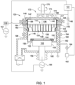
- the magnets 172 may be rotated about the shaft 176 to increase uniformity of the magnetic field across the surface of the sputtering target 142.
- the magnetron 170 is a small magnet magnetron.
- the magnets 172 may be both rotated and moved reciprocally in a linear direction parallel or substantially parallel to the face of the sputtering target 142 to produce a spiral motion.
- the magnets 172 may be rotated about both a central axis and an independently-controlled secondary axis to control both their radial and angular positions.
- the one-piece lower shield 180 encircles the sputtering surface 145 of the sputtering target 142 that faces the substrate support pedestal 152 and encircles a peripheral wall of the substrate support pedestal 152.
- the one-piece lower shield 180 covers and shadows the chamber wall 150 of the processing chamber 100 to reduce deposition of sputtering deposits originating from the sputtering surface 145 of the sputtering target 142 onto the components and surfaces behind the one-piece lower shield 180.
- the one-piece lower shield 180 can protect the surfaces of the substrate support pedestal 152, portions of the substrate 154, the chamber wall 150, and the bottom chamber wall 160 of the processing chamber 100.
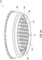
- FIG. 2A depicts a perspective view of a collimator assembly 108 in accordance with implementations of the present disclosure.
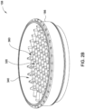
- FIG. 2B depicts another perspective view of the collimator assembly 108 in accordance with implementations of the present disclosure.
- FIG. 3 depicts a top view of the collimator assembly 108 of FIGS. 2A-2B that may be disposed in the processing chamber 100 of FIG. 1 .
- the collimator assembly 108 includes a one-piece upper shield portion 186 coupled with a collimator portion 110.
- the collimator portion 110 includes a plurality of apertures to direct gas and/or material flux within the processing chamber 100.
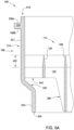
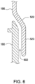
- the shield portion comprises a top ring, a support ledge below the top ring, the support ledge extending radially outward, and a cylindrical band extending downward from the support ledge.
- the cylindrical band has a first vertical or substantially vertical portion, a radially inwardly sloped portion extending downward from the first vertical or substantially vertical portion, and a second vertical or substantially vertical portion extending downward from the radially inward sloped portion, wherein the radially inward sloped portion extends across a portion of the second plurality of apertures in the peripheral region.
- the radially inward sloped portion extends across a portion of the second plurality of apertures in the peripheral region.
- the entrance angle portion has a predetermined angle of about 2.5 degrees and has a length of about 2.54 centimeters.
Landscapes
- Chemical & Material Sciences (AREA)
- Engineering & Computer Science (AREA)
- Physics & Mathematics (AREA)
- Plasma & Fusion (AREA)
- Analytical Chemistry (AREA)
- Materials Engineering (AREA)
- Chemical Kinetics & Catalysis (AREA)
- Mechanical Engineering (AREA)
- Metallurgy (AREA)
- Organic Chemistry (AREA)
- Physical Vapour Deposition (AREA)
- Electrodes Of Semiconductors (AREA)
- Physical Deposition Of Substances That Are Components Of Semiconductor Devices (AREA)
Applications Claiming Priority (4)
| Application Number | Priority Date | Filing Date | Title |
|---|---|---|---|
| US201562246967P | 2015-10-27 | 2015-10-27 | |
| EP21188409.3A EP3920210B1 (fr) | 2015-10-27 | 2016-09-27 | Dispositif d'optimisation/collimateur de flux pouvant être polarisé pour chambre de pulvérisation pvd |
| PCT/US2016/053970 WO2017074633A1 (fr) | 2015-10-27 | 2016-09-27 | Dispositif d'optimisation/collimateur de flux pouvant être polarisé pour chambre de pulvérisateur pvd |
| EP16860473.4A EP3369108B1 (fr) | 2015-10-27 | 2016-09-27 | Dispositif d'optimisation/collimateur de flux pouvant être polarisé pour chambre de pulvérisation pvd |
Related Parent Applications (2)
| Application Number | Title | Priority Date | Filing Date |
|---|---|---|---|
| EP21188409.3A Division EP3920210B1 (fr) | 2015-10-27 | 2016-09-27 | Dispositif d'optimisation/collimateur de flux pouvant être polarisé pour chambre de pulvérisation pvd |
| EP16860473.4A Division EP3369108B1 (fr) | 2015-10-27 | 2016-09-27 | Dispositif d'optimisation/collimateur de flux pouvant être polarisé pour chambre de pulvérisation pvd |
Publications (2)
| Publication Number | Publication Date |
|---|---|
| EP4235744A2 true EP4235744A2 (fr) | 2023-08-30 |
| EP4235744A3 EP4235744A3 (fr) | 2023-10-11 |
Family
ID=58562020
Family Applications (3)
| Application Number | Title | Priority Date | Filing Date |
|---|---|---|---|
| EP23175161.1A Pending EP4235744A3 (fr) | 2015-10-27 | 2016-09-27 | Dispositif d'optimisation/collimateur de flux pouvant être polarisé pour chambre de pulvérisation pvd |
| EP21188409.3A Active EP3920210B1 (fr) | 2015-10-27 | 2016-09-27 | Dispositif d'optimisation/collimateur de flux pouvant être polarisé pour chambre de pulvérisation pvd |
| EP16860473.4A Active EP3369108B1 (fr) | 2015-10-27 | 2016-09-27 | Dispositif d'optimisation/collimateur de flux pouvant être polarisé pour chambre de pulvérisation pvd |
Family Applications After (2)
| Application Number | Title | Priority Date | Filing Date |
|---|---|---|---|
| EP21188409.3A Active EP3920210B1 (fr) | 2015-10-27 | 2016-09-27 | Dispositif d'optimisation/collimateur de flux pouvant être polarisé pour chambre de pulvérisation pvd |
| EP16860473.4A Active EP3369108B1 (fr) | 2015-10-27 | 2016-09-27 | Dispositif d'optimisation/collimateur de flux pouvant être polarisé pour chambre de pulvérisation pvd |
Country Status (8)
| Country | Link |
|---|---|
| US (4) | US9960024B2 (fr) |
| EP (3) | EP4235744A3 (fr) |
| JP (3) | JP7034912B2 (fr) |
| KR (2) | KR102695398B1 (fr) |
| CN (6) | CN110438464A (fr) |
| SG (2) | SG10202003396PA (fr) |
| TW (5) | TWI669752B (fr) |
| WO (1) | WO2017074633A1 (fr) |
Families Citing this family (26)
| Publication number | Priority date | Publication date | Assignee | Title |
|---|---|---|---|---|
| KR102695398B1 (ko) | 2015-10-27 | 2024-08-13 | 어플라이드 머티어리얼스, 인코포레이티드 | Pvd 스퍼터 챔버를 위한 바이어스가능 플럭스 최적화기/콜리메이터 |
| CN109390222B (zh) * | 2017-08-08 | 2021-01-05 | 宁波江丰电子材料股份有限公司 | 准直器检具及其使用方法 |
| USD859333S1 (en) * | 2018-03-16 | 2019-09-10 | Applied Materials, Inc. | Collimator for a physical vapor deposition chamber |
| USD858468S1 (en) * | 2018-03-16 | 2019-09-03 | Applied Materials, Inc. | Collimator for a physical vapor deposition chamber |
| US20190353919A1 (en) * | 2018-05-21 | 2019-11-21 | Applied Materials, Inc. | Multi-zone collimator for selective pvd |
| CN109300764A (zh) * | 2018-10-31 | 2019-02-01 | 北京北方华创微电子装备有限公司 | 反应腔室及半导体加工设备 |
| WO2020088415A1 (fr) * | 2018-10-31 | 2020-05-07 | 北京北方华创微电子装备有限公司 | Chambre de réaction et dispositif de traitement de semi-conducteurs |
| USD937329S1 (en) | 2020-03-23 | 2021-11-30 | Applied Materials, Inc. | Sputter target for a physical vapor deposition chamber |
| USD998575S1 (en) | 2020-04-07 | 2023-09-12 | Applied Materials, Inc. | Collimator for use in a physical vapor deposition (PVD) chamber |
| CN112011776B (zh) * | 2020-08-28 | 2022-10-21 | 北京北方华创微电子装备有限公司 | 半导体工艺设备及其工艺腔室 |
| US11851751B2 (en) * | 2021-07-23 | 2023-12-26 | Taiwan Semiconductor Manufacturing Co., Ltd. | Deposition system and method |
| USD1009816S1 (en) | 2021-08-29 | 2024-01-02 | Applied Materials, Inc. | Collimator for a physical vapor deposition chamber |
| USD997111S1 (en) | 2021-12-15 | 2023-08-29 | Applied Materials, Inc. | Collimator for use in a physical vapor deposition (PVD) chamber |
| USD1038901S1 (en) | 2022-01-12 | 2024-08-13 | Applied Materials, Inc. | Collimator for a physical vapor deposition chamber |
| USD1026054S1 (en) | 2022-04-22 | 2024-05-07 | Applied Materials, Inc. | Collimator for a physical vapor deposition (PVD) chamber |
| CN115449762A (zh) * | 2022-08-22 | 2022-12-09 | 无锡尚积半导体科技有限公司 | 一种用于磁控溅射设备的准直器及磁控溅射设备 |
| USD1025935S1 (en) * | 2022-11-03 | 2024-05-07 | Applied Materials, Inc. | Collimator for a physical vapor deposition (PVD) chamber |
| USD1026839S1 (en) * | 2022-12-16 | 2024-05-14 | Applied Materials, Inc. | Collimator for a physical vapor deposition (PVD) chamber |
| USD1024149S1 (en) * | 2022-12-16 | 2024-04-23 | Applied Materials, Inc. | Collimator for a physical vapor deposition (PVD) chamber |
| USD1025936S1 (en) * | 2022-12-16 | 2024-05-07 | Applied Materials, Inc. | Collimator for a physical vapor deposition (PVD) chamber |
| CN119020736B (zh) * | 2023-05-24 | 2026-02-06 | 北京北方华创微电子装备有限公司 | 物理气相沉积设备的准直装置及物理气相沉积设备 |
| US20250146119A1 (en) * | 2023-11-07 | 2025-05-08 | Applied Materials, Inc. | Dual collimator physical vapor depositions processing chamber |
| WO2025181241A1 (fr) * | 2024-02-28 | 2025-09-04 | Université De Namur | Procédé de fabrication d'articles revêtus |
| USD1103950S1 (en) * | 2024-03-21 | 2025-12-02 | Applied Materials, Inc. | Process chamber collimator |
| USD1110979S1 (en) * | 2024-10-18 | 2026-02-03 | Applied Materials, Inc. | Process chamber collimator |
| USD1110289S1 (en) * | 2024-10-18 | 2026-01-27 | Applied Materials, Inc. | Process chamber collimator |
Family Cites Families (34)
| Publication number | Priority date | Publication date | Assignee | Title |
|---|---|---|---|---|
| US5223108A (en) * | 1991-12-30 | 1993-06-29 | Materials Research Corporation | Extended lifetime collimator |
| JPH06295903A (ja) * | 1993-02-09 | 1994-10-21 | Matsushita Electron Corp | スパッタリング装置 |
| US5380414A (en) | 1993-06-11 | 1995-01-10 | Applied Materials, Inc. | Shield and collimator pasting deposition chamber with a wafer support periodically used as an acceptor |
| US5362372A (en) | 1993-06-11 | 1994-11-08 | Applied Materials, Inc. | Self cleaning collimator |
| US5415753A (en) * | 1993-07-22 | 1995-05-16 | Materials Research Corporation | Stationary aperture plate for reactive sputter deposition |
| US5431799A (en) | 1993-10-29 | 1995-07-11 | Applied Materials, Inc. | Collimation hardware with RF bias rings to enhance sputter and/or substrate cavity ion generation efficiency |
| KR970009828B1 (en) | 1994-02-23 | 1997-06-18 | Sansung Electronics Co Ltd | Fabrication method of collimator |
| EP0703598A1 (fr) * | 1994-09-26 | 1996-03-27 | Applied Materials, Inc. | Electrode entre cible de pulvérisation et pièce à traiter |
| JPH08260139A (ja) * | 1995-03-23 | 1996-10-08 | Sony Corp | 成膜用コリメータ、成膜装置及び電子装置の製造方法 |
| KR970017999A (ko) * | 1995-09-29 | 1997-04-30 | 김광호 | 개선된 구조의 콜리메이터를 갖는 스퍼터링장치 |
| US5650052A (en) | 1995-10-04 | 1997-07-22 | Edelstein; Sergio | Variable cell size collimator |
| KR970017999U (ko) | 1995-10-23 | 1997-05-23 | 전자동세탁기 | |
| US5658442A (en) | 1996-03-07 | 1997-08-19 | Applied Materials, Inc. | Target and dark space shield for a physical vapor deposition system |
| US6482301B1 (en) | 1998-06-04 | 2002-11-19 | Seagate Technology, Inc. | Target shields for improved magnetic properties of a recording medium |
| US6362097B1 (en) | 1998-07-14 | 2002-03-26 | Applied Komatsu Technlology, Inc. | Collimated sputtering of semiconductor and other films |
| US6149776A (en) | 1998-11-12 | 2000-11-21 | Applied Materials, Inc. | Copper sputtering target |
| US20030015421A1 (en) | 2001-07-20 | 2003-01-23 | Applied Materials, Inc. | Collimated sputtering of cobalt |
| JP2005504885A (ja) | 2001-07-25 | 2005-02-17 | アプライド マテリアルズ インコーポレイテッド | 新規なスパッタ堆積方法を使用したバリア形成 |
| US20030029715A1 (en) | 2001-07-25 | 2003-02-13 | Applied Materials, Inc. | An Apparatus For Annealing Substrates In Physical Vapor Deposition Systems |
| US7048837B2 (en) | 2002-09-13 | 2006-05-23 | Applied Materials, Inc. | End point detection for sputtering and resputtering |
| TW200416838A (en) * | 2002-11-20 | 2004-09-01 | Renesas Tech Corp | Method of fabricating semiconductor device |
| JP2007273490A (ja) | 2004-03-30 | 2007-10-18 | Renesas Technology Corp | 半導体集積回路装置の製造方法 |
| EP1710324B1 (fr) | 2005-04-08 | 2008-12-03 | STMicroelectronics S.r.l. | Méthode et chambre de dépot PVD pulsé de chalcogénure pour des mémoires à changement de phase |
| US7355192B2 (en) * | 2006-03-30 | 2008-04-08 | Intel Corporation | Adjustable suspension assembly for a collimating lattice |
| JP5916384B2 (ja) | 2008-04-16 | 2016-05-11 | アプライド マテリアルズ インコーポレイテッドApplied Materials,Incorporated | ウェハ処理堆積物遮蔽構成材 |
| US9062379B2 (en) | 2008-04-16 | 2015-06-23 | Applied Materials, Inc. | Wafer processing deposition shielding components |
| US9316413B2 (en) | 2008-06-11 | 2016-04-19 | Honeywell International Inc. | Selectable efficiency versus comfort for modulating furnace |
| US20090308739A1 (en) * | 2008-06-17 | 2009-12-17 | Applied Materials, Inc. | Wafer processing deposition shielding components |
| US20090308732A1 (en) | 2008-06-17 | 2009-12-17 | Applied Materials, Inc. | Apparatus and method for uniform deposition |
| KR102374073B1 (ko) * | 2009-04-24 | 2022-03-11 | 어플라이드 머티어리얼스, 인코포레이티드 | 웨이퍼 프로세싱 증착 차폐 부품 |
| WO2013136384A1 (fr) * | 2012-03-14 | 2013-09-19 | キヤノンアネルバ株式会社 | Élément de fixation et dispositif sous vide |
| US9831074B2 (en) * | 2013-10-24 | 2017-11-28 | Applied Materials, Inc. | Bipolar collimator utilized in a physical vapor deposition chamber |
| US9543126B2 (en) | 2014-11-26 | 2017-01-10 | Applied Materials, Inc. | Collimator for use in substrate processing chambers |
| KR102695398B1 (ko) * | 2015-10-27 | 2024-08-13 | 어플라이드 머티어리얼스, 인코포레이티드 | Pvd 스퍼터 챔버를 위한 바이어스가능 플럭스 최적화기/콜리메이터 |
-
2016
- 2016-09-27 KR KR1020187014899A patent/KR102695398B1/ko active Active
- 2016-09-27 WO PCT/US2016/053970 patent/WO2017074633A1/fr not_active Ceased
- 2016-09-27 JP JP2018521365A patent/JP7034912B2/ja active Active
- 2016-09-27 SG SG10202003396PA patent/SG10202003396PA/en unknown
- 2016-09-27 EP EP23175161.1A patent/EP4235744A3/fr active Pending
- 2016-09-27 EP EP21188409.3A patent/EP3920210B1/fr active Active
- 2016-09-27 SG SG11201802667PA patent/SG11201802667PA/en unknown
- 2016-09-27 KR KR1020247026805A patent/KR20240127488A/ko active Pending
- 2016-09-27 EP EP16860473.4A patent/EP3369108B1/fr active Active
- 2016-09-27 US US15/277,674 patent/US9960024B2/en active Active
- 2016-10-27 TW TW105134741A patent/TWI669752B/zh active
- 2016-10-27 CN CN201910698016.7A patent/CN110438464A/zh active Pending
- 2016-10-27 CN CN201610958470.8A patent/CN106987815A/zh active Pending
- 2016-10-27 CN CN201621180242.4U patent/CN206418192U/zh active Active
- 2016-10-27 TW TW108124712A patent/TWI702636B/zh active
- 2016-10-27 CN CN202410177120.2A patent/CN118127471A/zh active Pending
- 2016-10-27 CN CN202010731212.2A patent/CN112030123A/zh active Pending
- 2016-10-27 TW TW111114403A patent/TWI839710B/zh active
- 2016-10-27 TW TW109124539A patent/TWI761889B/zh active
- 2016-10-27 CN CN202410177114.7A patent/CN118127470A/zh active Pending
- 2016-10-27 TW TW113110460A patent/TWI909376B/zh active
-
2018
- 2018-03-29 US US15/940,398 patent/US10347474B2/en active Active
-
2019
- 2019-05-30 US US16/426,964 patent/US10727033B2/en active Active
-
2020
- 2020-06-24 US US16/910,151 patent/US11309169B2/en active Active
-
2022
- 2022-03-02 JP JP2022031654A patent/JP7504938B2/ja active Active
-
2024
- 2024-06-12 JP JP2024095005A patent/JP2024127896A/ja active Pending
Also Published As
Similar Documents
| Publication | Publication Date | Title |
|---|---|---|
| US11309169B2 (en) | Biasable flux optimizer / collimator for PVD sputter chamber | |
| US9543126B2 (en) | Collimator for use in substrate processing chambers |
Legal Events
| Date | Code | Title | Description |
|---|---|---|---|
| PUAI | Public reference made under article 153(3) epc to a published international application that has entered the european phase |
Free format text: ORIGINAL CODE: 0009012 |
|
| STAA | Information on the status of an ep patent application or granted ep patent |
Free format text: STATUS: THE APPLICATION HAS BEEN PUBLISHED |
|
| AC | Divisional application: reference to earlier application |
Ref document number: 3369108 Country of ref document: EP Kind code of ref document: P Ref document number: 3920210 Country of ref document: EP Kind code of ref document: P |
|
| AK | Designated contracting states |
Kind code of ref document: A2 Designated state(s): AL AT BE BG CH CY CZ DE DK EE ES FI FR GB GR HR HU IE IS IT LI LT LU LV MC MK MT NL NO PL PT RO RS SE SI SK SM TR |
|
| REG | Reference to a national code |
Ref country code: DE Ref legal event code: R079 Free format text: PREVIOUS MAIN CLASS: H01J0037320000 Ipc: H01L0021285000 |
|
| PUAL | Search report despatched |
Free format text: ORIGINAL CODE: 0009013 |
|
| AK | Designated contracting states |
Kind code of ref document: A3 Designated state(s): AL AT BE BG CH CY CZ DE DK EE ES FI FR GB GR HR HU IE IS IT LI LT LU LV MC MK MT NL NO PL PT RO RS SE SI SK SM TR |
|
| RIC1 | Information provided on ipc code assigned before grant |
Ipc: H01J 37/32 20060101ALI20230901BHEP Ipc: H01J 37/34 20060101ALI20230901BHEP Ipc: C23C 14/16 20060101ALI20230901BHEP Ipc: H01L 21/768 20060101ALI20230901BHEP Ipc: H01L 21/285 20060101AFI20230901BHEP |
|
| STAA | Information on the status of an ep patent application or granted ep patent |
Free format text: STATUS: REQUEST FOR EXAMINATION WAS MADE |
|
| 17P | Request for examination filed |
Effective date: 20240409 |
|
| RBV | Designated contracting states (corrected) |
Designated state(s): AL AT BE BG CH CY CZ DE DK EE ES FI FR GB GR HR HU IE IS IT LI LT LU LV MC MK MT NL NO PL PT RO RS SE SI SK SM TR |