EP4235773A2 - Leitfähige dickschichtpaste für siliziumnitrid und andere substrate - Google Patents
Leitfähige dickschichtpaste für siliziumnitrid und andere substrate Download PDFInfo
- Publication number
- EP4235773A2 EP4235773A2 EP23176249.3A EP23176249A EP4235773A2 EP 4235773 A2 EP4235773 A2 EP 4235773A2 EP 23176249 A EP23176249 A EP 23176249A EP 4235773 A2 EP4235773 A2 EP 4235773A2
- Authority
- EP
- European Patent Office
- Prior art keywords
- thick film
- paste
- conductive thick
- conductive
- film paste
- Prior art date
- Legal status (The legal status is an assumption and is not a legal conclusion. Google has not performed a legal analysis and makes no representation as to the accuracy of the status listed.)
- Withdrawn
Links
Images

Classifications
-
- H—ELECTRICITY
- H05—ELECTRIC TECHNIQUES NOT OTHERWISE PROVIDED FOR
- H05K—PRINTED CIRCUITS; CASINGS OR CONSTRUCTIONAL DETAILS OF ELECTRIC APPARATUS; MANUFACTURE OF ASSEMBLAGES OF ELECTRICAL COMPONENTS
- H05K1/00—Printed circuits
- H05K1/02—Details
- H05K1/09—Use of materials for the conductive, e.g. metallic pattern
- H05K1/092—Dispersed materials, e.g. conductive pastes or inks
-
- B—PERFORMING OPERATIONS; TRANSPORTING
- B22—CASTING; POWDER METALLURGY
- B22F—WORKING METALLIC POWDER; MANUFACTURE OF ARTICLES FROM METALLIC POWDER; MAKING METALLIC POWDER; APPARATUS OR DEVICES SPECIALLY ADAPTED FOR METALLIC POWDER
- B22F1/00—Metallic powder; Treatment of metallic powder, e.g. to facilitate working or to improve properties
- B22F1/09—Mixtures of metallic powders
-
- B—PERFORMING OPERATIONS; TRANSPORTING
- B22—CASTING; POWDER METALLURGY
- B22F—WORKING METALLIC POWDER; MANUFACTURE OF ARTICLES FROM METALLIC POWDER; MAKING METALLIC POWDER; APPARATUS OR DEVICES SPECIALLY ADAPTED FOR METALLIC POWDER
- B22F10/00—Additive manufacturing of workpieces or articles from metallic powder
- B22F10/10—Formation of a green body
-
- B—PERFORMING OPERATIONS; TRANSPORTING
- B22—CASTING; POWDER METALLURGY
- B22F—WORKING METALLIC POWDER; MANUFACTURE OF ARTICLES FROM METALLIC POWDER; MAKING METALLIC POWDER; APPARATUS OR DEVICES SPECIALLY ADAPTED FOR METALLIC POWDER
- B22F7/00—Manufacture of composite layers, workpieces, or articles, comprising metallic powder, by sintering the powder, with or without compacting wherein at least one part is obtained by sintering or compression
- B22F7/02—Manufacture of composite layers, workpieces, or articles, comprising metallic powder, by sintering the powder, with or without compacting wherein at least one part is obtained by sintering or compression of composite layers
- B22F7/04—Manufacture of composite layers, workpieces, or articles, comprising metallic powder, by sintering the powder, with or without compacting wherein at least one part is obtained by sintering or compression of composite layers with one or more layers not made from powder, e.g. made from solid metal
-
- B—PERFORMING OPERATIONS; TRANSPORTING
- B33—ADDITIVE MANUFACTURING TECHNOLOGY
- B33Y—ADDITIVE MANUFACTURING, i.e. MANUFACTURING OF THREE-DIMENSIONAL [3D] OBJECTS BY ADDITIVE DEPOSITION, ADDITIVE AGGLOMERATION OR ADDITIVE LAYERING, e.g. BY 3D PRINTING, STEREOLITHOGRAPHY OR SELECTIVE LASER SINTERING
- B33Y10/00—Processes of additive manufacturing
-
- B—PERFORMING OPERATIONS; TRANSPORTING
- B33—ADDITIVE MANUFACTURING TECHNOLOGY
- B33Y—ADDITIVE MANUFACTURING, i.e. MANUFACTURING OF THREE-DIMENSIONAL [3D] OBJECTS BY ADDITIVE DEPOSITION, ADDITIVE AGGLOMERATION OR ADDITIVE LAYERING, e.g. BY 3D PRINTING, STEREOLITHOGRAPHY OR SELECTIVE LASER SINTERING
- B33Y80/00—Products made by additive manufacturing
-
- B—PERFORMING OPERATIONS; TRANSPORTING
- B41—PRINTING; LINING MACHINES; TYPEWRITERS; STAMPS
- B41M—PRINTING, DUPLICATING, MARKING, OR COPYING PROCESSES; COLOUR PRINTING
- B41M1/00—Inking and printing with a printer's forme
- B41M1/12—Stencil printing; Silk-screen printing
-
- B—PERFORMING OPERATIONS; TRANSPORTING
- B41—PRINTING; LINING MACHINES; TYPEWRITERS; STAMPS
- B41M—PRINTING, DUPLICATING, MARKING, OR COPYING PROCESSES; COLOUR PRINTING
- B41M1/00—Inking and printing with a printer's forme
- B41M1/26—Printing on other surfaces than ordinary paper
- B41M1/34—Printing on other surfaces than ordinary paper on glass or ceramic surfaces
-
- B—PERFORMING OPERATIONS; TRANSPORTING
- B41—PRINTING; LINING MACHINES; TYPEWRITERS; STAMPS
- B41M—PRINTING, DUPLICATING, MARKING, OR COPYING PROCESSES; COLOUR PRINTING
- B41M5/00—Duplicating or marking methods; Sheet materials for use therein
- B41M5/0023—Digital printing methods characterised by the inks used
-
- B—PERFORMING OPERATIONS; TRANSPORTING
- B41—PRINTING; LINING MACHINES; TYPEWRITERS; STAMPS
- B41M—PRINTING, DUPLICATING, MARKING, OR COPYING PROCESSES; COLOUR PRINTING
- B41M5/00—Duplicating or marking methods; Sheet materials for use therein
- B41M5/0041—Digital printing on surfaces other than ordinary paper
- B41M5/007—Digital printing on surfaces other than ordinary paper on glass, ceramic, tiles, concrete, stones, etc.
-
- C—CHEMISTRY; METALLURGY
- C09—DYES; PAINTS; POLISHES; NATURAL RESINS; ADHESIVES; COMPOSITIONS NOT OTHERWISE PROVIDED FOR; APPLICATIONS OF MATERIALS NOT OTHERWISE PROVIDED FOR
- C09D—COATING COMPOSITIONS, e.g. PAINTS, VARNISHES OR LACQUERS; FILLING PASTES; CHEMICAL PAINT OR INK REMOVERS; INKS; CORRECTING FLUIDS; WOODSTAINS; PASTES OR SOLIDS FOR COLOURING OR PRINTING; USE OF MATERIALS THEREFOR
- C09D17/00—Pigment pastes, e.g. for mixing in paints
- C09D17/004—Pigment pastes, e.g. for mixing in paints containing an inorganic pigment
- C09D17/006—Metal
-
- C—CHEMISTRY; METALLURGY
- C09—DYES; PAINTS; POLISHES; NATURAL RESINS; ADHESIVES; COMPOSITIONS NOT OTHERWISE PROVIDED FOR; APPLICATIONS OF MATERIALS NOT OTHERWISE PROVIDED FOR
- C09D—COATING COMPOSITIONS, e.g. PAINTS, VARNISHES OR LACQUERS; FILLING PASTES; CHEMICAL PAINT OR INK REMOVERS; INKS; CORRECTING FLUIDS; WOODSTAINS; PASTES OR SOLIDS FOR COLOURING OR PRINTING; USE OF MATERIALS THEREFOR
- C09D17/00—Pigment pastes, e.g. for mixing in paints
- C09D17/004—Pigment pastes, e.g. for mixing in paints containing an inorganic pigment
- C09D17/007—Metal oxide
-
- C—CHEMISTRY; METALLURGY
- C09—DYES; PAINTS; POLISHES; NATURAL RESINS; ADHESIVES; COMPOSITIONS NOT OTHERWISE PROVIDED FOR; APPLICATIONS OF MATERIALS NOT OTHERWISE PROVIDED FOR
- C09D—COATING COMPOSITIONS, e.g. PAINTS, VARNISHES OR LACQUERS; FILLING PASTES; CHEMICAL PAINT OR INK REMOVERS; INKS; CORRECTING FLUIDS; WOODSTAINS; PASTES OR SOLIDS FOR COLOURING OR PRINTING; USE OF MATERIALS THEREFOR
- C09D5/00—Coating compositions, e.g. paints, varnishes or lacquers, characterised by their physical nature or the effects produced; Filling pastes
- C09D5/24—Electrically-conducting paints
-
- H—ELECTRICITY
- H01—ELECTRIC ELEMENTS
- H01B—CABLES; CONDUCTORS; INSULATORS; SELECTION OF MATERIALS FOR THEIR CONDUCTIVE, INSULATING OR DIELECTRIC PROPERTIES
- H01B1/00—Conductors or conductive bodies characterised by the conductive materials; Selection of materials as conductors
- H01B1/20—Conductive material dispersed in non-conductive organic material
- H01B1/22—Conductive material dispersed in non-conductive organic material the conductive material comprising metals or alloys
-
- B—PERFORMING OPERATIONS; TRANSPORTING
- B22—CASTING; POWDER METALLURGY
- B22F—WORKING METALLIC POWDER; MANUFACTURE OF ARTICLES FROM METALLIC POWDER; MAKING METALLIC POWDER; APPARATUS OR DEVICES SPECIALLY ADAPTED FOR METALLIC POWDER
- B22F2301/00—Metallic composition of the powder or its coating
- B22F2301/10—Copper
-
- B—PERFORMING OPERATIONS; TRANSPORTING
- B22—CASTING; POWDER METALLURGY
- B22F—WORKING METALLIC POWDER; MANUFACTURE OF ARTICLES FROM METALLIC POWDER; MAKING METALLIC POWDER; APPARATUS OR DEVICES SPECIALLY ADAPTED FOR METALLIC POWDER
- B22F2301/00—Metallic composition of the powder or its coating
- B22F2301/25—Noble metals, i.e. Ag Au, Ir, Os, Pd, Pt, Rh, Ru
- B22F2301/255—Silver or gold
-
- B—PERFORMING OPERATIONS; TRANSPORTING
- B22—CASTING; POWDER METALLURGY
- B22F—WORKING METALLIC POWDER; MANUFACTURE OF ARTICLES FROM METALLIC POWDER; MAKING METALLIC POWDER; APPARATUS OR DEVICES SPECIALLY ADAPTED FOR METALLIC POWDER
- B22F2302/00—Metal Compound, non-Metallic compound or non-metal composition of the powder or its coating
- B22F2302/25—Oxide
-
- H—ELECTRICITY
- H05—ELECTRIC TECHNIQUES NOT OTHERWISE PROVIDED FOR
- H05K—PRINTED CIRCUITS; CASINGS OR CONSTRUCTIONAL DETAILS OF ELECTRIC APPARATUS; MANUFACTURE OF ASSEMBLAGES OF ELECTRICAL COMPONENTS
- H05K2201/00—Indexing scheme relating to printed circuits covered by H05K1/00
- H05K2201/02—Fillers; Particles; Fibers; Reinforcement materials
- H05K2201/0203—Fillers and particles
- H05K2201/0263—Details about a collection of particles
- H05K2201/0266—Size distribution
-
- H—ELECTRICITY
- H05—ELECTRIC TECHNIQUES NOT OTHERWISE PROVIDED FOR
- H05K—PRINTED CIRCUITS; CASINGS OR CONSTRUCTIONAL DETAILS OF ELECTRIC APPARATUS; MANUFACTURE OF ASSEMBLAGES OF ELECTRICAL COMPONENTS
- H05K2201/00—Indexing scheme relating to printed circuits covered by H05K1/00
- H05K2201/02—Fillers; Particles; Fibers; Reinforcement materials
- H05K2201/0203—Fillers and particles
- H05K2201/0263—Details about a collection of particles
- H05K2201/0272—Mixed conductive particles, i.e. using different conductive particles, e.g. differing in shape
-
- H—ELECTRICITY
- H10—SEMICONDUCTOR DEVICES; ELECTRIC SOLID-STATE DEVICES NOT OTHERWISE PROVIDED FOR
- H10W—GENERIC PACKAGES, INTERCONNECTIONS, CONNECTORS OR OTHER CONSTRUCTIONAL DETAILS OF DEVICES COVERED BY CLASS H10
- H10W70/00—Package substrates; Interposers; Redistribution layers [RDL]
- H10W70/60—Insulating or insulated package substrates; Interposers; Redistribution layers
- H10W70/62—Insulating or insulated package substrates; Interposers; Redistribution layers characterised by their interconnections
- H10W70/66—Conductive materials thereof
- H10W70/666—Organic materials or pastes
-
- H—ELECTRICITY
- H10—SEMICONDUCTOR DEVICES; ELECTRIC SOLID-STATE DEVICES NOT OTHERWISE PROVIDED FOR
- H10W—GENERIC PACKAGES, INTERCONNECTIONS, CONNECTORS OR OTHER CONSTRUCTIONAL DETAILS OF DEVICES COVERED BY CLASS H10
- H10W70/00—Package substrates; Interposers; Redistribution layers [RDL]
- H10W70/60—Insulating or insulated package substrates; Interposers; Redistribution layers
- H10W70/67—Insulating or insulated package substrates; Interposers; Redistribution layers characterised by their insulating layers or insulating parts
- H10W70/69—Insulating materials thereof
- H10W70/692—Ceramics or glasses
Definitions
- This invention relates to lead- and cadmium- free conductive copper thick film pastes for use in producing circuits and electronic devices on aluminum nitride, alumina and silicon nitride substrates.
- the thick film circuit is one well-known form of monolithic integrated microelectronic circuit. Circuits of this type are particularly useful where a large number of passive components are required, or where moderately high power dissipation is required. Thick film circuits are less costly to produce and, depending on composition and dimensional features, can yield a broader range of resistance values than thin film circuits.
- Thick film circuits consist of patterns of conductors, resistors and other passive circuit components printed on a particular substrate.
- a variety of pastes are applied onto a substrate or successive circuit layers through a screen or a template of a specific printed pattern. The successive layers are dried after printing and fired in a belt furnace to sinter the material.
- the substrate is often a ceramic material, such as alumina.
- a ceramic material such as alumina.
- other ceramic material with improved mechanical properties may be considered.
- thermal expansion coefficient may also be important.
- thick film pastes are typically compositions of glass particles, metal and/or metal oxide particles, together with organic solvents, resins and viscosity control agents known as thixotropes. The compositions of these thick film pastes depend upon the type of passive electrical component being printed.
- metal-containing thick film compositions i.e., pastes, inks, tapes, etc.
- resistors, dielectrics and conductors which are employed in hybrid microelectronic components have been developed in the field of hybrid microelectronics.
- compositions include a conductor (e.g., silver, palladium, copper, aluminum, gold, platinum, and the like as well as alloys of each of these different metals), resistive or dielectric components, a binder or an inorganic fluxing material, (e.g., a glass or inorganic oxides), and an organic components or vehicle comprising generally a solvent with a resin and a thixotrope and/or a wetting agent.
- a conductor e.g., silver, palladium, copper, aluminum, gold, platinum, and the like as well as alloys of each of these different metals
- resistive or dielectric components e.g., a resistive or dielectric components
- a binder or an inorganic fluxing material e.g., a glass or inorganic oxides
- organic components or vehicle comprising generally a solvent with a resin and a thixotrope and/or a wetting agent.
- the above-described paste or ink compositions are applied in the desired configuration or pattern onto a suitable substrate to form the desired circuit for use as a hybrid microelectronic component.
- a paste is a raw, unfired (green or "wet") mixture of glass and/or metal components together with an organic component (typically a binder or vehicle, and organic solvent).
- Silicon nitride has high strength and fracture toughness even at high temperatures. Therefore, it is used as high-temperature structural components for automotive engines, gas turbines, and combustor parts.
- silicon nitride is ideally suited for direct bonding of silicon-based circuit devices such as insulated-gate bipolar transistors (IGBT) used as electronic switches in high power circuits.
- IGBT insulated-gate bipolar transistors
- Packages of these devices often experience extreme temperature variations due to sudden changes of high electrical power.
- Silicon nitride's low coefficient of thermal expansion combined with high flexural strength and fairly high thermal conductivity make it suitable for applications requiring high thermal shock resistance.
- silicon nitride is a very non-reactive material
- a suitable metallic conductive thick film paste composition that is available to form circuits on a silicon nitride is not known.
- This disclosure provides details of screen printable metallic thick film paste compositions containing copper, silver and titanium metal powders suitable to form such circuits. Fired film showed very good electrical conductivity and adhesion to the substrate.
- Inkjet printing, digital printing and additive manufacturing (3D printing) application methods are also envisioned.
- Other processing techniques and conditions include; screen print, stencil printing, syringe deposition; One or two layers deposited by digital printing techniques; Firing atmospheres including ambient, Helium, Argon, Xenon, Neon, Krypton, Nitrogen (N 2 ) and combinations thereof. Layers may be fired individually or together. Multiple firings may be undertaken to build thickness of a finally fired component. Layers may be co-fired (1, 2, 3, or more).
- silicon nitride (SiNx or Si 3 N 4 ) substrates the present subject matter applies to AIN as well.
- Other substrates of interest include AIN, SiON, BN, and Alumina.
- the products of the invention may be used in MLCCs, LTCC, capacitors, resistors, cellular phones, computers, computer components, stereophonic equipment, home appliances, automotive components, televisions and other electronic products.
- Alloys containing Ag, Cu and Ti metal powders were identified as suitable candidates to bond Silicon nitride to other materials such as Silicon, stainless steel etc. These compositions are very fluid just above the melting point. Moreover, they are used only in vacuum or in Argon (inert) atmosphere.
- dried screen-printed patterns are fired in a belt furnace either in air or in N 2 atmosphere. Any composition that contains Cu as a part of conductor is fired in N 2 atmosphere.
- Industrial standard for thick film processing is 850-900°C. After firing, pattern dimensions in x-y directions should not change. The fired film should densify and bond very well to the substrate. If the formulation is intended for good electrical conductivity, the resistivity should be as low as possible, typically a few milli-ohms per square.
- compositions with Ag, Cu, and Ti powders were tested. Individual metal powder concentrations away from the eutectic region were selected to control the amount of liquid formation at 875-900°C. Compositions suitable for firing at 875-900°C in N 2 atmosphere with good adhesion and low electrical resistivity were identified.
- the bonding operation is carried out either in vacuum or in an inert atmosphere such as Argon.
- Typical active metal brazing alloy compositions are made with Ag-Cu eutectic with small amounts of active metal such as Ti.
- the present subject matter provides a lead-free and cadmium-free conductive thick film paste, comprising 20-40 wt.% first Cu (copper metal), 20-23 wt.% second Cu (copper metal), 3-12 wt.% Cu2O, 0.01-25 wt.% Ag, 0.01-25 wt.% of at least one metal element selected from Ti, V, Zr, Mn, Cr, Co, and Sn, and 5-20 wt.% organic component.
- the first Cu has a D50 particle size in microns about 2-12, 3-11, 4-10, 5-9, 6-8 and ranges not specified that are between values selected from the ranges in this sentence.
- the first Cu has a D50 particle size in microns of about 0.01-8, 0.01- 5, or 0.5 to 3 or ranges not specified that are between values selected from the ranges in this sentence.
- a second Cu has a D50 particle size in microns in the range of about 12-30, 14-27, 16-25, 17-24, 18-23, 19-22, 20-21 and ranges not specified that are between values selected from the ranges in this sentence.
- the second Cu has a D50 particle size in microns of about 0.01-8, 0.01- 5, or 0.5 to 3 or ranges not specified that are between values selected from the ranges in this sentence.
- a second Cu has a D50 particle size in microns in ranges of about 12-30, 14-27, 16-25, 17-24, 18-23, 19-22, 20-21 and ranges not specified that are between values selected from the ranges in this sentence.
- a paste is an unfired composition.
- the present subject matter provides a lead-free and cadmium-free conductive thick film paste including a glass component and a copper (Cu) component.
- the glass component includes 15-65 wt.% alkaline earth oxide, 0.01-10 wt.% alkali oxide, 22-70 wt.% (B 2 O 3 +SiO 2 ), and 0.01-15 wt.% Al 2 O 3 .
- the alkaline earth oxide is selected from the group consisting of MgO, CaO, SrO, BaO, and ZnO.
- the alkali oxide is selected from the group consisting of Li 2 O, Na 2 O, K 2 O, and Rb 2 O.
- the present subject matter provides a method of forming a conductive thick film on a substrate.
- the method includes applying at least one layer of a first conductive thick film paste and a second conductive thick film to form a conductive thick film on the substrate.
- the first conductive thick film paste includes in wt.% 20-40 wt.% first Cu, 20-23 wt.% second Cu, 3-12 wt.% Cu 2 O, 0.01-25 wt.% Ag, 0.01-25 wt.% at least one metal element selected from Ti, V, Zr, Mn, Cr, Co, and Sn, and 12-20 wt.% organic component.
- the first Cu has a D50 particle size in microns about 2 up to12, 3-11, 4-10, 5-9, 6-8 and ranges not specified that are between values selected from the ranges in this sentence.
- a second Cu has a D50 particle size in microns about 12-30, 14-27, 16-25, 17-24, 18-23, 19-22, 20-21 and ranges not specified that are between values selected from the ranges in this sentence.
- the second conductive thick film paste includes a glass component and a copper (Cu) component.
- the glass component includes 15-65 wt.% alkaline earth oxide, 0.01-10 wt.% alkali oxide, 22-70 wt.% (B 2 O 3 +SiO 2 ), and 0.01-15 wt.% Al 2 O 3 .
- the alkaline earth oxide is selected from the group consisting of MgO, CaO, SrO, and BaO.
- ZnO may be included in the alkaline earth oxide component. Oxides of Ca, Ba, and Zn are preferred, and oxides of Ca and Zn are most preferred.
- the alkali oxide is selected from the group consisting of Li 2 O, Na 2 O, K 2 O, and Rb 2 O and combinations thereof.
- the method further includes drying the first and second conductive thick film pastes on the substrate.
- the method further includes firing the dried first conductive thick film paste and the dried second conductive thick film paste to form the fired conductive thick film on the substrate.
- the substrate is selected from the group consisting of aluminum oxide, aluminum nitride, silicon nitride, and boron nitride.
- the present subject matter provides an electronic device including a substrate, and a fired conductive thick film disposed on at least a portion of the substrate.
- the fired conductive thick film includes at least one first fired conductive thick film and one second fired conductive thick film.
- the substrate is selected from the group consisting of aluminum oxide, aluminum nitride, and silicon nitride.
- the first fired conductive thick film includes the conductive thick film paste including 20-40 wt.% first Cu, 20-23 wt.% second Cu, 3-12 wt.% Cu 2 O, 0.01-25 wt.% Ag, 0.01-25 wt.% at least a metal element selected from Ti, V, Zr, Mn, Cr, Co, and Sn, and 12-20 wt.% organic component.
- the first Cu has a D50 particle size in microns about 2-12, 3-11, 4-10, 5-9, 6-8 and ranges not specified that are between values selected from the ranges in this sentence.
- a second Cu has a D50 particle size in microns about 12-30, 14-27, 16-25, 17-24, 18-23, 19-22, 20-21 and ranges not specified that are between values selected from the ranges in this sentence.
- the second fired conductive thick film includes the conductive thick film paste including a glass component and a copper (Cu) component.
- the glass component includes 15-65 wt.% alkaline earth oxide, 0.01-10 wt.% alkali oxide, 22-70 wt.% (B 2 O 3 +SiO 2 ), and 0.01-15 wt.% Al 2 O 3 .
- the alkaline earth oxide is selected from the group consisting of MgO, CaO, SrO, BaO, and ZnO.
- the alkali oxide is selected from the group consisting of Li 2 O, Na 2 O, K 2 O, and Rb 2 O.
- the present invention provides a lead-free and cadmium-free conductive thick film paste, which contains copper, for use in producing hybrid microelectronic components across a wide temperature range.
- This thick film paste including copper is formed on aluminum oxide, aluminum nitride, and silicon nitride without suffering sintering and includes a glass component that flows at relatively low firing temperatures.
- the automotive industry, the optoelectronics industry, or military requires a plurality of silicon based circuit devices in the electronic systems.
- One of the silicon based circuit devices include, for example, an insulated-gate-bipolar-transistors (IGBT) used as electronic switches in high power circuits.
- IGBT insulated-gate-bipolar-transistors
- the electronic systems including the IGBT from time to time requires experiencing extreme temperature variations due to sudden changes of high electric power.
- IGBTs are fabricated on a ceramic substrate such as aluminum oxide (alumina) and aluminum nitride.
- a thin layer of copper is metallized on the alumina substrate.
- inventive thick films possess additional desirable characteristics such as good solderability (i.e., excellent solder wetting), good wire bondability, low resistivity, and provide excellent adhesion to a variety of substrates, including 96% alumina and glass coated stainless steel substrates, as well as low resistivity, and a microstructure after firing that is dense and substantially free of pores.
- Copper is an ideal conductor material for thick film and power electronic applications because it has a high electrical conductivity, high thermal conductivity, resists solder leaching, and resists electro migration much better than other conductors such as silver, and can handle a high current density.
- Prior art low-temperature firing copper thick film systems exhibit minimal adhesion to common substrates, poor solderability and often contain undesirable metals such as lead or cadmium.
- the inventive paste compositions are conductive. While the line between conductors and resistors is often unclear, the paste compositions of the present invention have a sheet resistivity of about 2.1-3.1 miliohm / sq / mil. And maximum resistivity of about 20 milliOhms per square (mOhm/square).
- the present subject matter also provides an electronic device having a lead-free and cadmium-free conductive thick film applied thereto and fired to form an electrical circuit.
- Electronic devices upon which the lead-free and cadmium-free conductive thick film can be applied and fired include direct bonding of silicon based circuit devices such as insulated-gate-bipolar-transistors (IGBT), which is used as electronic switches in high power circuits.
- IGBT insulated-gate-bipolar-transistors
- the term "electronic device” means any electronic device that includes thick film and/or hybrid thick film circuitry that would survive at least the firing temperatures disclosed herein and benefit from the conductive circuitry provided by the lead-free and cadmium-free thick film paste composition.
- the present subject matter provides a lead- and cadmium-free conductive thick film pastes having at least Cu a metal component and a glass component.
- the metal component comprises copper.
- the glass component comprises a first glass and a second glass, and is free of lead, cadmium and compounds of lead and cadmium.
- the lead-free and cadmium-free conductive thick film paste of the present subject matter is generally applied to a surface of an electronic device upon which has been formed one or more circuits or other electronic components (e.g., transistors, capacitors, and resistors).
- the conductive thick film paste is preferably dried and fired, as is more thoroughly described below, to form a lead and cadmium free electrical circuit on the substrate.
- the phrase "lead-free and cadmium-free" means that no lead, or PbO, cadmium, or CdO, has been intentionally added to the composition, and that the composition comprises less than about 0.1% by weight Pb or Cd after firing.
- the inventive conductive thick film paste may be applied to a substrate by means of screen printing, syringe deposition, and digital printing technique.
- the paste may contain an organic components or vehicle, providing appropriate viscosity in order to pass through the screen.
- the paste may also contain a thixotropic material in order to set up rapidly after being screened to give good resolution. While the rheological properties are of primary importance, the organic components is preferably formulated also to give appropriate wettability of the solids and the substrate, good drying rate, dried film strength sufficient to withstand rough handling, and good firing properties. Satisfactory appearance of the fired composition is also important.
- the organic components for most conductive thick film pastes is typically a solution of a resin dissolved in a solvent and, frequently, a solvent solution containing both resin and a thixotropic agent.
- the solvent usually boils within the range of about 130°C to about 350°C.
- the most frequently used resin for this purpose is ethyl cellulose.
- resins such as ethyl hydroxy ethyl cellulose, wood rosin, mixtures of ethyl cellulose and phenolic resins, polymethacrylates of lower alcohols and monobutyl ether of ethylene glycol monoacetate can also be used.
- solvents for thick film applications are terpenes such as alpha- or beta-terpineol or mixtures thereof with other solvents such as kerosene, dibutyl phthalate, butyl carbitol, butyl carbitol acetate, hexylene glycol, texanol, and high-boiling alcohols and alcohol esters.
- solvents such as kerosene, dibutyl phthalate, butyl carbitol, butyl carbitol acetate, hexylene glycol, texanol, and high-boiling alcohols and alcohol esters.
- thixotropic agents organic based thixotropes such as, for example, hydrogenated castor oil and derivatives thereof. It is of course, not always necessary to incorporate a thixotropic agent because the solvent/resin properties coupled with the sheer thinning inherent in any suspension may alone be suitable in this regard.
- a wetting agent may be employed such as fatty acid esters, e.g., N-tallow-1,3-diaminopropane di-oleate, N-tallow trimethylene diamine diacetate, N-coco trimethylene diamine, beta diamines, N-oleyl trimethylene diamine, N-tallow trimethylene diamine, and/or N-tallow trimethylene diamine dioleate.
- the ratio of organic components to solids in the inventive conductive compositions may vary considerably and is dependent upon the manner in which the conductive compositions are to be applied and the type of organic components used. Normally to achieve good coverage, the conductive composition may contain by weight 60-90% solids and 40-10% of a liquid organic components. Such conductive compositions are usually of semi-fluid consistency and are referred to commonly as "pastes.”
- the first conductive thick film paste preferably contains from about 75% to about 94% by weight solids and from about 6 to about 25% by weight of the liquid organic components.
- the preferred ranges of components in the solids portion for the first conductive thick film paste according to the present subject matter is as follows (Table 1) : a) a first copper, preferably from about 20.0 to about 40.0 %, more preferably from about 20.0 to about 36.0 %, most preferably from about 23.0 to about 29.0 % of the first conductive thick film paste; b) a second copper, preferably from about 20.0 to about 36.0 %, more preferably from about 20.0 to about 30.0 %, most preferably from about 20.0 to about 25.0 % of the first conductive thick film paste; c) cuprous oxide (Cu 2 O) comprising, preferably from about 0.01 to about 12.0 %, more preferably from about 4.0 to about 12.0 %, most preferably from about 4.0 to about 9.0 % of the first
- the at least one metal element is selected from the group consisting of Ti, V, Zr, Mn, Cr, Co, and Sn. In a preferred embodiment, the at least one metal element is selected from the group selected from Ti, V, Zr, Cr, and Sn. In a more preferred embodiment, the at least a metal element is selected from the group selected from Ti, and Sn. In a most preferred embodiment, the at least a metal element is Ti. Table 1. Solid portion of first conductive thick film paste Composition Preferred More Preferred Most Preferred First Cu 20-40 20-36 23-29 Second Cu 20-36 20-30 20-25 Cuprous oxide (Cu 2 O) 0.01-12 4-12 4-9 Silver (Ag) 0.01-25 2-20 8-17 Metal element 0.01-25 1-20 10-16
- the preferred composition according to the present invention is as follows: 1) at least about 90 percent by weight organic solvent; 2) up to about 15 percent by weight resin; 3) up to about 4 percent by weight thixotropic agent; and 4) up to about 2 percent by weight wetting agent.
- Exemplary vehicles are EV2803, 235 and No flow m7 all available from Ferro Corporation which consist of ethyl cellulose dissolved in Terpineol and Texanol.
- the copper metal is advantageously provided in the form of powders and/or flakes.
- the second conductive thick film paste preferably contains from about 70% to about 94% by weight solids and from about 8 to about 30% by weight of the liquid organic components.
- the preferred ranges of components in the solids portion for the second conductive thick film paste according to the present subject matter is as follows (Table 2) : a) a first copper, preferably from about 14 to about 23%, more preferably from about 15 to about 23%, most preferably from about 17 to about 22% of the second conductive thick film paste; b) a second copper, preferably from about 20 to about 28%, more preferably from about 22 to about 28%, most preferably from about 23 to about 26% of the second conductive thick film paste; c) a third copper, preferably from about 15 to about 24%, more preferably from about 15 to about 24%, most preferably from about 18 to about 24% of the second conductive thick film paste; and d) cuprous oxide (Cu 2 O) comprising, preferably from about 0.1 to about 11%, more preferably from about
- the solids portion for the second conductive thick film paste also includes the glass component usually provided initially in the form of one or more glass powders.
- the present subject matter provides a conductive thick film paste, said paste including a Pb- and Cd- free glass component, said glass component comprising in mole%: about 15 to about 65% alkaline earth oxide, about 0.01 to about 10% alkali oxide, about 22 to about 70% (B 2 O 3 + SiO 2 ), and about 0.01 to about 15% Al 2 O 3 .
- At least one alkaline earth oxide is selected from MgO, CaO, SrO, BaO, and ZnO.
- at least one alkaline earth oxide is selected from MgO, CaO, and ZnO.
- at least one alkaline earth oxide is selected from CaO, and ZnO.
- At least one alkali oxide is selected from Li 2 O, Na 2 O, K 2 O, and Rb 2 O.
- compositional ranges are preferred and it is not the intention to be limited to these ranges where one of ordinary skill in the art would recognize that these ranges may vary depending upon specific applications, specific components and conditions for processing and forming the end products.
- a numerical range bounded by zero at the lower end the disclosure is also read as having a value of 0.01 or 0.1 at the lower end.
- the paste according to the present invention may be conveniently prepared on a three-roll mill.
- the amount and type of organic components utilized are determined mainly by the final desired formulation viscosity, fineness of grind of the paste, and wet print thickness.
- the particulate inorganic solids are mixed with the organic components and dispersed with suitable equipment, such as a three-roll mill, to form a suspension, resulting in a composition for which the viscosity will be in the range of about 50 to about 200 kcps, preferably about 100 to about 150 kcps, at a shear rate of 9.6 sec -1 as determined on a Brookfield viscometer 2HBT, spindle CP-51, measured at 25°C.
- the circuit substrates according to the present subject matter are preferably produced by applying the first conductive thick film paste of the present subject matter to a substrate, usually by the process of screen printing, to a desired wet thickness, e.g., from about 60 to about 80 microns. Automatic screen printing techniques can be employed using a 80-325 mesh screen.
- the printed pattern is then dried at below 200°C, e.g., preferably at about 175°C for about 20-40 minutes.
- the second conductive thick film paste of the present subject matter is applied to the top of the dried first conductive thick film paste.
- the printed pattern is then dried at below 200°C, e.g., preferably at about 175°C for about 20-40 minutes before firing.
- the glass is fused and the metal is sintered in a controlled, non-oxidizing atmosphere belt conveyor furnace.
- the firing is generally done according to a temperature profile that will allow burnout of the organic matter at about 300°C to about 550°C, a period of peak temperature of about 850°C to about 1050°C, lasting about 5-15 minutes, followed by a controlled cool-down cycle to prevent over-sintering, unwanted chemical reactions at intermediate temperatures or substrate fracture, which can occur when the substrate cools too quickly.
- a non-oxidizing atmosphere such as nitrogen, argon or mixtures thereof is used to prevent oxidation of metal, especially copper, which tends to oxidize in air even at room temperature.
- a nitrogen atmosphere is preferred.
- the amount of oxygen in nitrogen may be preferably controlled to lower than 10 ppm.
- the overall firing procedure will preferably extend over a period of about 60 to 85 minutes, with about 25 to 30 minutes to reach the firing temperature, about 5 to 15 minutes at the firing temperature, and about 30 to 40 minutes in cool down.
- An exemplary firing cycle is, assuming room temperature of 20°C, ramp up at about 30°C/min to a peak temperature of 900°C, holding at 900°C for 12 minutes, and cooling at 60°C/min for about 15 minutes to exit the furnace at about 60°C.
- Conductive thick film pastes include the first conductive thick film paste and the second conductive thick film paste.
- the first conductive thick film paste is formed directly on the top of the substrate, and the second conductive thick film paste is formed directly on the top of the first conductive thick film paste, where the first conductive thick film paste is in a dry state.
- First conductive thick film paste was made by mixing appropriate amounts of copper powders with two (2) different particle sizes, silver powders, cuprous oxide (Cu 2 O) powders, at least a metal element, Boric acid, Triton X-100, Ethanox 702 with organic vehicles, first in a planetary mixer for homogenization, and next in a three-roll mill to achieve a fineness of grind of less than 50, preferably ⁇ 40, more preferably ⁇ 30, still more preferably ⁇ 20, even more preferably ⁇ 10 ⁇ m.
- Second conductive thick film paste was made by mixing copper powders with three (3) different particle sizes, Cu 2 O powders, and glass powders, boric acid, Triton X-100, Ethanox 702 with organic vehicles, first in a planetary mixer for homogenization, and next in a three-roll mill to achieve a fineness of grind of less than 20 ⁇ m.
- the viscosity of the first and second conductive thick film pastes was measured with a Brookfield HBT viscometer 2HB, 2.5 rpm at 25 °C using spindle CP-51. Shelf life of the green pastes is good.
- the second conductive thick film paste includes Pb free and Cd free glass powder.
- the glass powder formulation includes about 15-65% of alkaline earth oxide, about 0.01-10 wt.% of alkali oxide, about 22-70 wt.% of (B 2 O 3 +SiO 2 ), and about 0.01-15 wt.% of Al 2 O 3 .
- the alkaline earth oxide is one or more selected from the group consisting of MgO, CaO, SrO, BaO, and ZnO.
- the alkali oxide is one or more selected from the group consisting of Li 2 O, Na 2 O, K 2 O, and Rb 2 O.
- Suitable commercially available glasses from Ferro Corporation include, EG0026, EG0028, EG2807, EG3046, LF256; EG2810, BBS2.
- the metal component comprises copper metal.
- Copper metal typically is provided in the form of at least one of powder and/or flakes.
- Copper powders may have a plurality of copper powders having different particle size distribution and/or particle morphology.
- more than one size range of copper particles may be used for the first and second conductive thick film pastes, respectively.
- the copper powder may include a first copper powder having D50 of about 5 micron, and a specific surface area (SSA).
- the first copper powder is sold under the name ICP UF-5-AC, and available from Makin-UK.
- a second copper powder has D50 of about 0.3-0.5 micron.
- the second copper powder is sold under the product name CU-F400 available from CNPC.
- the copper powder may include a first copper powder having D50 of about 5 micron.
- the first copper powder is sold under the name ICP UF-5-AC, and available from Makin-UK.
- a second copper powder has D50 of about 1.5 micron, and specific surface area (SSA) of 0.65 m 2 /g.
- the second copper powder is sold under Cu 22-201, and available from Technic Corporation.
- a third copper powder has D50 of about 10 micron.
- the third copper powder is sold under Cu-APC0412000CX00, and available from Safina Corporation.
- the first conductive thick film includes flake shaped silver (Ag) powder with D50 of less than 9 micron.
- the specific surface area (SSA) ranges 0.65-1.35 m 2 /g.
- the Ag powder is sold under Silver Flake SF-4, available from Ames Corporation.
- the Titanium (Ti) powder has D100 of less than 20 micron, and is sold under Ti-101, available from AEE Corporation.
- Commercially available Cuprous oxide (Cu 2 O) is used in forming both the first and second conducive thick films.
- substrates used were: (1) silicon nitride (Maruwa, Japan), (2) aluminum nitride (Maruwa, Japan), and (3) 96% alumina (CoorsTek, USA).
- the first conductive thick film pastes were screen printed on the substrates using 80 mesh screens and a pattern appropriate for testing resistivity and adhesion.
- the printed pastes are dried in a box oven at 175°C for 30 minutes.
- the second conductive thick film pastes were screen printed on the dried first conductive thick film pastes using 80 mesh screens and a pattern appropriate for testing resistivity and adhesion.
- the printed second conductive thick film pastes are dried in the box oven at 175°C for 30 minutes.
- the thickness of the green screen-printed paste was about 80-120 ⁇ m and upon drying decreased to 50-65 ⁇ m.
- thicknesses are possible in various embodiments, such as green thicknesses in microns of 10-50 (with 325 mesh screen), 70-130, 75-125, 85-115, 90-110, 95-105, and ranges not specified that are between values selected from the ranges in this sentence.
- Other possible fired thicknesses in various embodiments such as fired thicknesses in microns of 5-25, 40-90, 45-85, 50-80, 55-75, 60-70, and ranges with upper and lower bounds selected from the ranges in this sentence.
- Firing profile and conditions A belt furnace was used, with a belt speed of 1.88 inches (4.78 cm) per minute. The sample was heated to peak temperature over the course of 28 minutes. The sample was held at the peak temperature for 10-30 minutes. The sample was cooled at a controlled rate to about 60°C, this cooling requiring about 38 minutes. Samples were fired in a nitrogen atmosphere having less than 10 ppm O 2 . Peak temperature was 650°C, or 1050°C, or other values in between.
- Testing performed included electrical characteristics, initial adhesion to substrate, and aged adhesion to substrate. Electrical testing included determination of resistivity, expressed in mOhm/square, calculated from the measured resistance of a serpentine pattern that is 500 micron wide having 200 squares and a fired thickness of about 30 ⁇ m, then normalized to 25.4 ⁇ m.
- Adhesion was measured by dip soldering, in which a 22 AWG Cu-Sn wire was soldered to a 0.080" by 0.080" square pad using 62Sn/36Pb/2Ag solder and KESTER ® RMA solder flux 197.
- KESTER ® is the registered trademark of Kester Solder, Des Plaines, III. 60018-2675.
- the wires were then pulled at 90° to failure using the Shepard Crook method.
- Adhesion strength was expressed as pounds of force needed to break the wire. Aged adhesion was measured after subjecting the soldered joint to a temperature of 150°C for 48 hours.
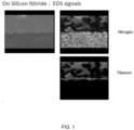
- Fig. 1 shows that Ti is detected as a continuous layer at the interface, and indicates an interfacial reaction and bonding to the substrates.
- the fired paste is above the reaction zone, and the substrate is below the reaction zone.
- Example 1 The compositions of inventive thick film pastes, paste A, paste B, and paste C are described in Table 3. Silicon nitride and aluminum nitride were used as substrates. Either paste A or paste B is formed directly on the substrate as an adhesion layer. After either paste A or paste B is dried, Paste C is formed on the either paste A or paste B. It is noted that the detailed composition of paste A and paste B are slightly different from each other to tailor the adhesion of Cu thick film on the substrate. After paste C is dried, the dried conductive thick film stack was fired in a N 2 atmosphere at 900°C. Selected electrical and mechanical properties of the stack including paste C on paste A, after firing on silicon nitride and aluminum nitride, are shown in Table 4.
- an aged adhesion of at least 3 pounds of force is considered to be acceptable for thick films formed on a substrate.
- Aged adhesion was above the acceptable level, and was in the range of 5-6 pounds force, which is promising for use for an extended period.
- Sheet resistivity of the fired conductive thick film was in the range of 2.1 to 3.1 mOhm/square. Considering that typically 1-5 mOhm/square is considered to be a good conductor, it is expected that the conductive thick film according to the present subject matter would work as thick film circuitry on silicon nitride and aluminum nitride. Table 3.
- compositions for Pastes A, B, and C Pastes Ingredients A B C First Cu powder 23-29 23-29 14-23 Second Cu powder 20-25 20-25 - Second Cu powder - - 20-28 Third Cu powder - - 15-24 Cuprous oxide (Cu 2 O) 4-9 4-9 5-11 Ag 8-17 8-17 - Metal element 10-16 10-16 - Glass - - 1-10 Boric acid 0.60 0.60 0.68 Triton X-100 1.40 1.40 1.49 Irganox 1076 0.10 Ethanox 702 0.40 0.40 No flow m7 8.20 7.70 8.69 Vehicle EV2803 - - 0.60 Vehicle 235 INT 6.40 7.50 9.07 Hexylene Glycol 0.30 0.20 0.48 Texanol - - 1.48 Table 4.
- Example 2 The inventive thick film pastes B and C in Table 3 were selected to form a thick film stack. Silicon nitride, aluminum nitride, and alumina were used as substrates. Thick film pastes B and C are formed on each substrate such that the paste B is in direct contact with the substrate. After paste B is dried at a similar temperature as paste A in Example 1, paste C is formed on the paste B and dried. The thick film stack was fired in an N 2 atmosphere at 900°C. Selected electrical and mechanical properties of the fired conductive thick film stack are shown in Table 5. Sheet resistivity of the fired conductive thick film was, regardless of the substrate used, in the range of 3.0 and 3.1 mOhm/square, and was in acceptable range as electrically conductive circuitry.
- the conductive thick film stack according to the present subject matter showed improved adhesion (both initial and aged) on silicon nitride substrate over other substrates including aluminum nitride and alumina.
- the Invention is further defined by the following Items.
- Item A-1 A lead-free and cadmium-free conductive thick film paste comprising in wt.%:
- Item A-4 The thick film paste of any of items A-1 or A-2 or A-3, further comprising an organic components portion, the paste comprising by weight from about 10 to about 20% organic components portion.
- a lead-free and cadmium-free conductive thick film paste comprising a glass component and a copper (Cu) component, the glass component in wt.% comprising:
- Item B-2 The thick film paste of item B-1, wherein the alkaline earth oxide is selected from MgO, CaO, and ZnO.
- Item B-3 The thick film paste of item B-2 or item B-2, wherein the alkaline earth oxide is selected from CaO, and ZnO.
- Item B-4 The thick film paste of any of items B-1, B-2 or B-3, wherein D50 of the glass component is from about 0.5 to about 20 micron.
- Item B-5 The thick film paste of any of items B-1, B-2, B-3, or B-4 wherein the Cu comprises in wt.%:
- Item B-6 The thick film paste of item B-1, wherein the Cu comprises in wt.%:
- Item B-7 The thick film paste of item B-1, further comprising a organic components portion, the paste comprising by weight from about 10 to about 30% organic components portion.
- a method of forming a fired conductive thick film on a substrate comprising:
- Item C-2 The method of item C-1, wherein the at least one of the conductive thick film paste of any of items A-1 through A-4, and the conductive thick film paste any of items B-1 through B-7 is applied by one selected from the group consisting of additive manufacturing, screen printing, syringe deposition, and digital printing technique.
- Item C-3 The method of item C-1 or C-2, wherein the firing is conducted at a temperature of from about 850 to about 1050 °C.
- Item C-4 The method of any of items C-1 through C-3, wherein the firing is conducted at a temperature of from about 850 to about 900 °C.
- Item C-5 The method of any of items C-1 through C-4, wherein the atmosphere contains less than 10 parts per million (ppm) oxygen.
- Item C-6 The method of any of items C-1 through C-4, wherein the firing is conducted in a reducing atmosphere.
- Item C-7 The method of any of items C-1 through C-6, wherein the reducing atmosphere comprises nitrogen (N2).
- An electronic device comprising:
- Item D-2 The electronic device of item D-1, wherein an interface comprising nitrogen is formed between the substrate and the lead-free and cadmium-free conductive thick film.
- Item D-3 The electronic device of item D-1 or item D-2, wherein the interface further comprises Ti.
- Item D-4 The electronic device of any of items D-1 through D-3, wherein the first conductive thick film is disposed directly on the substrate.
- Item D-5 The electronic device of any of items D-1 through D-4, wherein the second conductive thick film is disposed on the first conductive thick film.
- Item D-6 The electronic device of any of items D-1 through D-5, wherein the lead-free and cadmium-free conductive thick film is formed by firing at a temperature of from about 850 to about 1050 °C.
- the thick film pastes of the present invention may be utilized in conjunction with a variety of substrates, including but not limited to porcelain enamel coated steel, beryllia substrates, glass substrates, barium titanate substrates, silicon substrate, boron nitride substrate, and silicon carbide substrates. Additionally, it will be appreciated that in addition to the screen printing technique utilized in the previous Examples, the thick film pastes of the present invention may be applied using a variety of additional techniques known in the art including spraying, brushing, dipping, ink-jet or doctor blade.
- glass as used herein is intended to be afforded a broad interpretation and thus it encompasses both glasses, and glass-ceramics that display some degree of crystallization.
- the present invention is summarized by the following items:
Landscapes
- Chemical & Material Sciences (AREA)
- Engineering & Computer Science (AREA)
- Materials Engineering (AREA)
- Manufacturing & Machinery (AREA)
- Organic Chemistry (AREA)
- Life Sciences & Earth Sciences (AREA)
- Wood Science & Technology (AREA)
- Dispersion Chemistry (AREA)
- Inorganic Chemistry (AREA)
- Ceramic Engineering (AREA)
- Microelectronics & Electronic Packaging (AREA)
- Composite Materials (AREA)
- Mechanical Engineering (AREA)
- Physics & Mathematics (AREA)
- Spectroscopy & Molecular Physics (AREA)
- Parts Printed On Printed Circuit Boards (AREA)
- Conductive Materials (AREA)
- Manufacturing Of Electric Cables (AREA)
- Production Of Multi-Layered Print Wiring Board (AREA)
Applications Claiming Priority (3)
| Application Number | Priority Date | Filing Date | Title |
|---|---|---|---|
| US201862728382P | 2018-09-07 | 2018-09-07 | |
| PCT/US2019/049838 WO2020051390A1 (en) | 2018-09-07 | 2019-09-06 | Conductive thick film paste for silicon nitride and other substrates |
| EP19858462.5A EP3824481B1 (de) | 2018-09-07 | 2019-09-06 | Leitfähige dickschichtpaste für siliziumnitrid und andere substrate |
Related Parent Applications (2)
| Application Number | Title | Priority Date | Filing Date |
|---|---|---|---|
| EP19858462.5A Division-Into EP3824481B1 (de) | 2018-09-07 | 2019-09-06 | Leitfähige dickschichtpaste für siliziumnitrid und andere substrate |
| EP19858462.5A Division EP3824481B1 (de) | 2018-09-07 | 2019-09-06 | Leitfähige dickschichtpaste für siliziumnitrid und andere substrate |
Publications (2)
| Publication Number | Publication Date |
|---|---|
| EP4235773A2 true EP4235773A2 (de) | 2023-08-30 |
| EP4235773A3 EP4235773A3 (de) | 2023-10-04 |
Family
ID=69723221
Family Applications (2)
| Application Number | Title | Priority Date | Filing Date |
|---|---|---|---|
| EP23176249.3A Withdrawn EP4235773A3 (de) | 2018-09-07 | 2019-09-06 | Leitfähige dickschichtpaste für siliziumnitrid und andere substrate |
| EP19858462.5A Active EP3824481B1 (de) | 2018-09-07 | 2019-09-06 | Leitfähige dickschichtpaste für siliziumnitrid und andere substrate |
Family Applications After (1)
| Application Number | Title | Priority Date | Filing Date |
|---|---|---|---|
| EP19858462.5A Active EP3824481B1 (de) | 2018-09-07 | 2019-09-06 | Leitfähige dickschichtpaste für siliziumnitrid und andere substrate |
Country Status (6)
| Country | Link |
|---|---|
| US (1) | US20220225501A1 (de) |
| EP (2) | EP4235773A3 (de) |
| JP (1) | JP7256260B2 (de) |
| CN (1) | CN112673435B (de) |
| TW (1) | TWI717004B (de) |
| WO (1) | WO2020051390A1 (de) |
Families Citing this family (2)
| Publication number | Priority date | Publication date | Assignee | Title |
|---|---|---|---|---|
| CN113948236B (zh) * | 2021-12-21 | 2022-03-29 | 西安宏星电子浆料科技股份有限公司 | 一种耐磨损高精度油位传感器用厚膜银钯导体浆料 |
| TWI870684B (zh) * | 2022-07-22 | 2025-01-21 | 凱鍶科技股份有限公司 | 抗氧化導電散熱銅漿黏著劑及其製造方法 |
Family Cites Families (19)
| Publication number | Priority date | Publication date | Assignee | Title |
|---|---|---|---|---|
| JPH0346705A (ja) * | 1989-07-14 | 1991-02-28 | Showa Denko Kk | 銅ペースト |
| JP3507084B2 (ja) * | 1991-12-13 | 2004-03-15 | イー・アイ・デュポン・ドウ・ヌムール・アンド・カンパニー | 銅導体組成物 |
| JPH07135394A (ja) * | 1993-11-09 | 1995-05-23 | Ngk Spark Plug Co Ltd | 厚膜コンデンサ付きセラミック配線基板及びその製造方法 |
| JP3756283B2 (ja) * | 1997-03-31 | 2006-03-15 | 三ツ星ベルト株式会社 | 窒化アルミ基板用銅導体ペースト及び窒化アルミ基板 |
| EP1598364A1 (de) * | 2004-05-21 | 2005-11-23 | AGIRx Limited | Chimerischer löslicher Hyper IL-11 Rezeptor und dessen Verwendung |
| US7176152B2 (en) * | 2004-06-09 | 2007-02-13 | Ferro Corporation | Lead-free and cadmium-free conductive copper thick film pastes |
| US7326367B2 (en) * | 2005-04-25 | 2008-02-05 | E.I. Du Pont De Nemours And Company | Thick film conductor paste compositions for LTCC tape in microwave applications |
| CN101816045A (zh) * | 2007-10-18 | 2010-08-25 | E.I.内穆尔杜邦公司 | 无铅导电组合物以及用于制造半导体装置的方法:含镁添加剂 |
| CN102270513B (zh) * | 2010-06-03 | 2013-05-08 | 西安宏星电子浆料科技有限责任公司 | 氧化铝基板使用的厚膜导体浆料及其制备方法 |
| US9374892B1 (en) * | 2011-11-01 | 2016-06-21 | Triton Microtechnologies | Filling materials and methods of filling through holes for improved adhesion and hermeticity in glass substrates and other electronic components |
| EP2706538A3 (de) * | 2012-09-10 | 2014-04-23 | Heraeus Precious Metals North America Conshohocken LLC | Kupferzusammensetzung mit niedriger Brenntemperatur |
| US9236155B2 (en) * | 2013-02-04 | 2016-01-12 | E I Du Pont De Nemours And Company | Copper paste composition and its use in a method for forming copper conductors on substrates |
| EP2804183B1 (de) * | 2013-05-14 | 2019-04-17 | Fraunhofer-Gesellschaft zur Förderung der Angewandten Forschung e.V. | Braunrote Cu-haltige Zusammensetzung und ein Kompositmaterial mit der braunroten Cu-haltigen Zusammensetzung |
| US9799421B2 (en) * | 2013-06-07 | 2017-10-24 | Heraeus Precious Metals North America Conshohocken Llc | Thick print copper pastes for aluminum nitride substrates |
| US9666731B2 (en) * | 2013-10-21 | 2017-05-30 | Samsung Sdi Co., Ltd. | Composition for solar cell electrodes, electrode fabricated using the same, and solar cell having the electrode |
| EP3093319A1 (de) * | 2015-05-13 | 2016-11-16 | Heraeus Deutschland GmbH & Co. KG | Elektrisch leitfähige zusammensetzung |
| JP6354970B2 (ja) * | 2015-10-01 | 2018-07-11 | 昭栄化学工業株式会社 | 導電性ペースト及び積層セラミック部品の端子電極形成方法 |
| JP6569545B2 (ja) | 2016-01-27 | 2019-09-04 | 住友金属鉱山株式会社 | 厚膜銅電極または配線とその形成方法 |
| US11183315B2 (en) * | 2016-08-03 | 2021-11-23 | Shoei Chemical Inc. | Conductive paste |
-
2019
- 2019-09-06 WO PCT/US2019/049838 patent/WO2020051390A1/en not_active Ceased
- 2019-09-06 EP EP23176249.3A patent/EP4235773A3/de not_active Withdrawn
- 2019-09-06 TW TW108132248A patent/TWI717004B/zh active
- 2019-09-06 CN CN201980058397.0A patent/CN112673435B/zh not_active Expired - Fee Related
- 2019-09-06 EP EP19858462.5A patent/EP3824481B1/de active Active
- 2019-09-06 JP JP2021512377A patent/JP7256260B2/ja active Active
- 2019-09-06 US US17/272,736 patent/US20220225501A1/en not_active Abandoned
Also Published As
| Publication number | Publication date |
|---|---|
| JP2021536676A (ja) | 2021-12-27 |
| CN112673435A (zh) | 2021-04-16 |
| EP3824481B1 (de) | 2023-11-08 |
| EP3824481A1 (de) | 2021-05-26 |
| US20220225501A1 (en) | 2022-07-14 |
| EP3824481A4 (de) | 2022-08-03 |
| TWI717004B (zh) | 2021-01-21 |
| EP4235773A3 (de) | 2023-10-04 |
| JP7256260B2 (ja) | 2023-04-11 |
| CN112673435B (zh) | 2023-01-06 |
| WO2020051390A1 (en) | 2020-03-12 |
| TW202015073A (zh) | 2020-04-16 |
Similar Documents
| Publication | Publication Date | Title |
|---|---|---|
| US7504349B2 (en) | Lead-free and cadmium-free conductive copper thick film pastes | |
| US4172919A (en) | Copper conductor compositions containing copper oxide and Bi2 O3 | |
| US7611645B2 (en) | Thick film conductor compositions and the use thereof in LTCC circuits and devices | |
| JP5303552B2 (ja) | セラミック基板用導体ペーストおよび電気回路 | |
| US5165986A (en) | Copper conductive composition for use on aluminum nitride substrate | |
| JPH0350365B2 (de) | ||
| CN101238531B (zh) | 用于电容器的含有无铅无镉玻璃的铜端电极油墨 | |
| US20100200283A1 (en) | Insulation paste for a metal core substrate and electronic device | |
| US4871608A (en) | High-density wiring multilayered substrate | |
| EP3824481B1 (de) | Leitfähige dickschichtpaste für siliziumnitrid und andere substrate | |
| JP2002163928A (ja) | ガラス組成物およびこれを用いた厚膜ペースト | |
| CA1165994A (en) | Thick film conductor compositions | |
| US4567151A (en) | Binder glass of Bi2 O3 -SiO2 -GeO2 (-PbO optional) admixed with ZnO/ZnO and Bi2 O3 | |
| US5120473A (en) | Metallizing composition for use with ceramics | |
| KR102851511B1 (ko) | 후막 저항 페이스트, 후막 저항체, 및 전자 부품 | |
| JPH0455536B2 (de) |
Legal Events
| Date | Code | Title | Description |
|---|---|---|---|
| PUAI | Public reference made under article 153(3) epc to a published international application that has entered the european phase |
Free format text: ORIGINAL CODE: 0009012 |
|
| STAA | Information on the status of an ep patent application or granted ep patent |
Free format text: STATUS: THE APPLICATION HAS BEEN PUBLISHED |
|
| REG | Reference to a national code |
Ref country code: DE Ref legal event code: R079 Free format text: PREVIOUS MAIN CLASS: H01L0023498000 Ipc: H01B0001220000 |
|
| AC | Divisional application: reference to earlier application |
Ref document number: 3824481 Country of ref document: EP Kind code of ref document: P |
|
| AK | Designated contracting states |
Kind code of ref document: A2 Designated state(s): AL AT BE BG CH CY CZ DE DK EE ES FI FR GB GR HR HU IE IS IT LI LT LU LV MC MK MT NL NO PL PT RO RS SE SI SK SM TR |
|
| PUAL | Search report despatched |
Free format text: ORIGINAL CODE: 0009013 |
|
| AK | Designated contracting states |
Kind code of ref document: A3 Designated state(s): AL AT BE BG CH CY CZ DE DK EE ES FI FR GB GR HR HU IE IS IT LI LT LU LV MC MK MT NL NO PL PT RO RS SE SI SK SM TR |
|
| RIC1 | Information provided on ipc code assigned before grant |
Ipc: H01L 23/498 20060101ALI20230828BHEP Ipc: H01L 23/15 20060101ALI20230828BHEP Ipc: H05K 1/09 20060101ALI20230828BHEP Ipc: H05K 3/12 20060101ALI20230828BHEP Ipc: H01B 13/00 20060101ALI20230828BHEP Ipc: H01B 12/06 20060101ALI20230828BHEP Ipc: H01B 1/22 20060101AFI20230828BHEP |
|
| STAA | Information on the status of an ep patent application or granted ep patent |
Free format text: STATUS: REQUEST FOR EXAMINATION WAS MADE |
|
| P01 | Opt-out of the competence of the unified patent court (upc) registered |
Effective date: 20231022 |
|
| 17P | Request for examination filed |
Effective date: 20231106 |
|
| RBV | Designated contracting states (corrected) |
Designated state(s): AL AT BE BG CH CY CZ DE DK EE ES FI FR GB GR HR HU IE IS IT LI LT LU LV MC MK MT NL NO PL PT RO RS SE SI SK SM TR |
|
| STAA | Information on the status of an ep patent application or granted ep patent |
Free format text: STATUS: THE APPLICATION HAS BEEN WITHDRAWN |
|
| 17Q | First examination report despatched |
Effective date: 20240208 |
|
| 18W | Application withdrawn |
Effective date: 20240205 |
|
| RAP3 | Party data changed (applicant data changed or rights of an application transferred) |
Owner name: VIBRANTZ CORPORATION |