EP4235783A2 - Dispositifs de circuit intégré comprenant des éléments empilés et leurs procédés de formation - Google Patents
Dispositifs de circuit intégré comprenant des éléments empilés et leurs procédés de formation Download PDFInfo
- Publication number
- EP4235783A2 EP4235783A2 EP23157586.1A EP23157586A EP4235783A2 EP 4235783 A2 EP4235783 A2 EP 4235783A2 EP 23157586 A EP23157586 A EP 23157586A EP 4235783 A2 EP4235783 A2 EP 4235783A2
- Authority
- EP
- European Patent Office
- Prior art keywords
- substrate
- bonding pad
- bonding
- integrated circuit
- circuit device
- Prior art date
- Legal status (The legal status is an assumption and is not a legal conclusion. Google has not performed a legal analysis and makes no representation as to the accuracy of the status listed.)
- Pending
Links
Images






Classifications
-
- H—ELECTRICITY
- H10—SEMICONDUCTOR DEVICES; ELECTRIC SOLID-STATE DEVICES NOT OTHERWISE PROVIDED FOR
- H10D—INORGANIC ELECTRIC SEMICONDUCTOR DEVICES
- H10D84/00—Integrated devices formed in or on semiconductor substrates that comprise only semiconducting layers, e.g. on Si wafers or on GaAs-on-Si wafers
- H10D84/80—Integrated devices formed in or on semiconductor substrates that comprise only semiconducting layers, e.g. on Si wafers or on GaAs-on-Si wafers characterised by the integration of at least one component covered by groups H10D12/00 or H10D30/00, e.g. integration of IGFETs
- H10D84/811—Combinations of field-effect devices and one or more diodes, capacitors or resistors
-
- H—ELECTRICITY
- H10—SEMICONDUCTOR DEVICES; ELECTRIC SOLID-STATE DEVICES NOT OTHERWISE PROVIDED FOR
- H10W—GENERIC PACKAGES, INTERCONNECTIONS, CONNECTORS OR OTHER CONSTRUCTIONAL DETAILS OF DEVICES COVERED BY CLASS H10
- H10W20/00—Interconnections in chips, wafers or substrates
- H10W20/40—Interconnections external to wafers or substrates, e.g. back-end-of-line [BEOL] metallisations or vias connecting to gate electrodes
- H10W20/41—Interconnections external to wafers or substrates, e.g. back-end-of-line [BEOL] metallisations or vias connecting to gate electrodes characterised by their conductive parts
- H10W20/427—Power or ground buses
-
- H—ELECTRICITY
- H10—SEMICONDUCTOR DEVICES; ELECTRIC SOLID-STATE DEVICES NOT OTHERWISE PROVIDED FOR
- H10W—GENERIC PACKAGES, INTERCONNECTIONS, CONNECTORS OR OTHER CONSTRUCTIONAL DETAILS OF DEVICES COVERED BY CLASS H10
- H10W90/00—Package configurations
-
- H—ELECTRICITY
- H10—SEMICONDUCTOR DEVICES; ELECTRIC SOLID-STATE DEVICES NOT OTHERWISE PROVIDED FOR
- H10D—INORGANIC ELECTRIC SEMICONDUCTOR DEVICES
- H10D84/00—Integrated devices formed in or on semiconductor substrates that comprise only semiconducting layers, e.g. on Si wafers or on GaAs-on-Si wafers
- H10D84/01—Manufacture or treatment
- H10D84/0123—Integrating together multiple components covered by H10D12/00 or H10D30/00, e.g. integrating multiple IGBTs
- H10D84/0126—Integrating together multiple components covered by H10D12/00 or H10D30/00, e.g. integrating multiple IGBTs the components including insulated gates, e.g. IGFETs
- H10D84/0149—Manufacturing their interconnections or electrodes, e.g. source or drain electrodes
-
- H—ELECTRICITY
- H10—SEMICONDUCTOR DEVICES; ELECTRIC SOLID-STATE DEVICES NOT OTHERWISE PROVIDED FOR
- H10D—INORGANIC ELECTRIC SEMICONDUCTOR DEVICES
- H10D84/00—Integrated devices formed in or on semiconductor substrates that comprise only semiconducting layers, e.g. on Si wafers or on GaAs-on-Si wafers
- H10D84/01—Manufacture or treatment
- H10D84/02—Manufacture or treatment characterised by using material-based technologies
- H10D84/03—Manufacture or treatment characterised by using material-based technologies using Group IV technology, e.g. silicon technology or silicon-carbide [SiC] technology
- H10D84/038—Manufacture or treatment characterised by using material-based technologies using Group IV technology, e.g. silicon technology or silicon-carbide [SiC] technology using silicon technology, e.g. SiGe
-
- H—ELECTRICITY
- H10—SEMICONDUCTOR DEVICES; ELECTRIC SOLID-STATE DEVICES NOT OTHERWISE PROVIDED FOR
- H10D—INORGANIC ELECTRIC SEMICONDUCTOR DEVICES
- H10D88/00—Three-dimensional [3D] integrated devices
-
- H—ELECTRICITY
- H10—SEMICONDUCTOR DEVICES; ELECTRIC SOLID-STATE DEVICES NOT OTHERWISE PROVIDED FOR
- H10P—GENERIC PROCESSES OR APPARATUS FOR THE MANUFACTURE OR TREATMENT OF DEVICES COVERED BY CLASS H10
- H10P50/00—Etching of wafers, substrates or parts of devices
-
- H—ELECTRICITY
- H10—SEMICONDUCTOR DEVICES; ELECTRIC SOLID-STATE DEVICES NOT OTHERWISE PROVIDED FOR
- H10W—GENERIC PACKAGES, INTERCONNECTIONS, CONNECTORS OR OTHER CONSTRUCTIONAL DETAILS OF DEVICES COVERED BY CLASS H10
- H10W20/00—Interconnections in chips, wafers or substrates
- H10W20/40—Interconnections external to wafers or substrates, e.g. back-end-of-line [BEOL] metallisations or vias connecting to gate electrodes
- H10W20/41—Interconnections external to wafers or substrates, e.g. back-end-of-line [BEOL] metallisations or vias connecting to gate electrodes characterised by their conductive parts
- H10W20/42—Vias, e.g. via plugs
-
- H—ELECTRICITY
- H10—SEMICONDUCTOR DEVICES; ELECTRIC SOLID-STATE DEVICES NOT OTHERWISE PROVIDED FOR
- H10W—GENERIC PACKAGES, INTERCONNECTIONS, CONNECTORS OR OTHER CONSTRUCTIONAL DETAILS OF DEVICES COVERED BY CLASS H10
- H10W20/00—Interconnections in chips, wafers or substrates
- H10W20/40—Interconnections external to wafers or substrates, e.g. back-end-of-line [BEOL] metallisations or vias connecting to gate electrodes
- H10W20/41—Interconnections external to wafers or substrates, e.g. back-end-of-line [BEOL] metallisations or vias connecting to gate electrodes characterised by their conductive parts
- H10W20/435—Cross-sectional shapes or dispositions of interconnections
-
- H—ELECTRICITY
- H10—SEMICONDUCTOR DEVICES; ELECTRIC SOLID-STATE DEVICES NOT OTHERWISE PROVIDED FOR
- H10W—GENERIC PACKAGES, INTERCONNECTIONS, CONNECTORS OR OTHER CONSTRUCTIONAL DETAILS OF DEVICES COVERED BY CLASS H10
- H10W72/00—Interconnections or connectors in packages
- H10W72/90—Bond pads, in general
-
- H—ELECTRICITY
- H10—SEMICONDUCTOR DEVICES; ELECTRIC SOLID-STATE DEVICES NOT OTHERWISE PROVIDED FOR
- H10W—GENERIC PACKAGES, INTERCONNECTIONS, CONNECTORS OR OTHER CONSTRUCTIONAL DETAILS OF DEVICES COVERED BY CLASS H10
- H10W80/00—Direct bonding of chips, wafers or substrates
-
- H—ELECTRICITY
- H10—SEMICONDUCTOR DEVICES; ELECTRIC SOLID-STATE DEVICES NOT OTHERWISE PROVIDED FOR
- H10W—GENERIC PACKAGES, INTERCONNECTIONS, CONNECTORS OR OTHER CONSTRUCTIONAL DETAILS OF DEVICES COVERED BY CLASS H10
- H10W80/00—Direct bonding of chips, wafers or substrates
- H10W80/301—Bonding techniques, e.g. hybrid bonding
-
- H—ELECTRICITY
- H10—SEMICONDUCTOR DEVICES; ELECTRIC SOLID-STATE DEVICES NOT OTHERWISE PROVIDED FOR
- H10W—GENERIC PACKAGES, INTERCONNECTIONS, CONNECTORS OR OTHER CONSTRUCTIONAL DETAILS OF DEVICES COVERED BY CLASS H10
- H10W80/00—Direct bonding of chips, wafers or substrates
- H10W80/701—Direct bonding of chips, wafers or substrates characterised by the pads after the direct bonding
-
- H—ELECTRICITY
- H10—SEMICONDUCTOR DEVICES; ELECTRIC SOLID-STATE DEVICES NOT OTHERWISE PROVIDED FOR
- H10W—GENERIC PACKAGES, INTERCONNECTIONS, CONNECTORS OR OTHER CONSTRUCTIONAL DETAILS OF DEVICES COVERED BY CLASS H10
- H10W90/00—Package configurations
- H10W90/701—Package configurations characterised by the relative positions of pads or connectors relative to package parts
- H10W90/791—Package configurations characterised by the relative positions of pads or connectors relative to package parts of direct-bonded pads
- H10W90/792—Package configurations characterised by the relative positions of pads or connectors relative to package parts of direct-bonded pads between multiple chips
-
- H—ELECTRICITY
- H10—SEMICONDUCTOR DEVICES; ELECTRIC SOLID-STATE DEVICES NOT OTHERWISE PROVIDED FOR
- H10W—GENERIC PACKAGES, INTERCONNECTIONS, CONNECTORS OR OTHER CONSTRUCTIONAL DETAILS OF DEVICES COVERED BY CLASS H10
- H10W99/00—Subject matter not provided for in other groups of this subclass
-
- H—ELECTRICITY
- H10—SEMICONDUCTOR DEVICES; ELECTRIC SOLID-STATE DEVICES NOT OTHERWISE PROVIDED FOR
- H10D—INORGANIC ELECTRIC SEMICONDUCTOR DEVICES
- H10D84/00—Integrated devices formed in or on semiconductor substrates that comprise only semiconducting layers, e.g. on Si wafers or on GaAs-on-Si wafers
- H10D84/201—Integrated devices formed in or on semiconductor substrates that comprise only semiconducting layers, e.g. on Si wafers or on GaAs-on-Si wafers characterised by the integration of only components covered by H10D1/00 or H10D8/00, e.g. RLC circuits
- H10D84/204—Integrated devices formed in or on semiconductor substrates that comprise only semiconducting layers, e.g. on Si wafers or on GaAs-on-Si wafers characterised by the integration of only components covered by H10D1/00 or H10D8/00, e.g. RLC circuits of combinations of diodes or capacitors or resistors
-
- H—ELECTRICITY
- H10—SEMICONDUCTOR DEVICES; ELECTRIC SOLID-STATE DEVICES NOT OTHERWISE PROVIDED FOR
- H10D—INORGANIC ELECTRIC SEMICONDUCTOR DEVICES
- H10D84/00—Integrated devices formed in or on semiconductor substrates that comprise only semiconducting layers, e.g. on Si wafers or on GaAs-on-Si wafers
- H10D84/60—Integrated devices formed in or on semiconductor substrates that comprise only semiconducting layers, e.g. on Si wafers or on GaAs-on-Si wafers characterised by the integration of at least one component covered by groups H10D10/00 or H10D18/00, e.g. integration of BJTs
- H10D84/611—Combinations of BJTs and one or more of diodes, resistors or capacitors
- H10D84/613—Combinations of vertical BJTs and one or more of diodes, resistors or capacitors
- H10D84/615—Combinations of vertical BJTs and one or more of resistors or capacitors
-
- H—ELECTRICITY
- H10—SEMICONDUCTOR DEVICES; ELECTRIC SOLID-STATE DEVICES NOT OTHERWISE PROVIDED FOR
- H10D—INORGANIC ELECTRIC SEMICONDUCTOR DEVICES
- H10D84/00—Integrated devices formed in or on semiconductor substrates that comprise only semiconducting layers, e.g. on Si wafers or on GaAs-on-Si wafers
- H10D84/80—Integrated devices formed in or on semiconductor substrates that comprise only semiconducting layers, e.g. on Si wafers or on GaAs-on-Si wafers characterised by the integration of at least one component covered by groups H10D12/00 or H10D30/00, e.g. integration of IGFETs
- H10D84/82—Integrated devices formed in or on semiconductor substrates that comprise only semiconducting layers, e.g. on Si wafers or on GaAs-on-Si wafers characterised by the integration of at least one component covered by groups H10D12/00 or H10D30/00, e.g. integration of IGFETs of only field-effect components
- H10D84/83—Integrated devices formed in or on semiconductor substrates that comprise only semiconducting layers, e.g. on Si wafers or on GaAs-on-Si wafers characterised by the integration of at least one component covered by groups H10D12/00 or H10D30/00, e.g. integration of IGFETs of only field-effect components of only insulated-gate FETs [IGFET]
- H10D84/837—Integrated devices formed in or on semiconductor substrates that comprise only semiconducting layers, e.g. on Si wafers or on GaAs-on-Si wafers characterised by the integration of at least one component covered by groups H10D12/00 or H10D30/00, e.g. integration of IGFETs of only field-effect components of only insulated-gate FETs [IGFET] comprising vertical IGFETs
-
- H—ELECTRICITY
- H10—SEMICONDUCTOR DEVICES; ELECTRIC SOLID-STATE DEVICES NOT OTHERWISE PROVIDED FOR
- H10D—INORGANIC ELECTRIC SEMICONDUCTOR DEVICES
- H10D84/00—Integrated devices formed in or on semiconductor substrates that comprise only semiconducting layers, e.g. on Si wafers or on GaAs-on-Si wafers
- H10D84/80—Integrated devices formed in or on semiconductor substrates that comprise only semiconducting layers, e.g. on Si wafers or on GaAs-on-Si wafers characterised by the integration of at least one component covered by groups H10D12/00 or H10D30/00, e.g. integration of IGFETs
- H10D84/82—Integrated devices formed in or on semiconductor substrates that comprise only semiconducting layers, e.g. on Si wafers or on GaAs-on-Si wafers characterised by the integration of at least one component covered by groups H10D12/00 or H10D30/00, e.g. integration of IGFETs of only field-effect components
- H10D84/83—Integrated devices formed in or on semiconductor substrates that comprise only semiconducting layers, e.g. on Si wafers or on GaAs-on-Si wafers characterised by the integration of at least one component covered by groups H10D12/00 or H10D30/00, e.g. integration of IGFETs of only field-effect components of only insulated-gate FETs [IGFET]
- H10D84/85—Complementary IGFETs, e.g. CMOS
-
- H—ELECTRICITY
- H10—SEMICONDUCTOR DEVICES; ELECTRIC SOLID-STATE DEVICES NOT OTHERWISE PROVIDED FOR
- H10W—GENERIC PACKAGES, INTERCONNECTIONS, CONNECTORS OR OTHER CONSTRUCTIONAL DETAILS OF DEVICES COVERED BY CLASS H10
- H10W72/00—Interconnections or connectors in packages
- H10W72/01—Manufacture or treatment
- H10W72/019—Manufacture or treatment of bond pads
-
- H—ELECTRICITY
- H10—SEMICONDUCTOR DEVICES; ELECTRIC SOLID-STATE DEVICES NOT OTHERWISE PROVIDED FOR
- H10W—GENERIC PACKAGES, INTERCONNECTIONS, CONNECTORS OR OTHER CONSTRUCTIONAL DETAILS OF DEVICES COVERED BY CLASS H10
- H10W72/00—Interconnections or connectors in packages
- H10W72/01—Manufacture or treatment
- H10W72/019—Manufacture or treatment of bond pads
- H10W72/01904—Manufacture or treatment of bond pads using temporary auxiliary members, e.g. using sacrificial coatings or handle substrates
-
- H—ELECTRICITY
- H10—SEMICONDUCTOR DEVICES; ELECTRIC SOLID-STATE DEVICES NOT OTHERWISE PROVIDED FOR
- H10W—GENERIC PACKAGES, INTERCONNECTIONS, CONNECTORS OR OTHER CONSTRUCTIONAL DETAILS OF DEVICES COVERED BY CLASS H10
- H10W72/00—Interconnections or connectors in packages
- H10W72/90—Bond pads, in general
- H10W72/931—Shapes of bond pads
- H10W72/934—Cross-sectional shape, i.e. in side view
-
- H—ELECTRICITY
- H10—SEMICONDUCTOR DEVICES; ELECTRIC SOLID-STATE DEVICES NOT OTHERWISE PROVIDED FOR
- H10W—GENERIC PACKAGES, INTERCONNECTIONS, CONNECTORS OR OTHER CONSTRUCTIONAL DETAILS OF DEVICES COVERED BY CLASS H10
- H10W72/00—Interconnections or connectors in packages
- H10W72/90—Bond pads, in general
- H10W72/941—Dispositions of bond pads
- H10W72/942—Dispositions of bond pads relative to underlying supporting features, e.g. bond pads, RDLs or vias
-
- H—ELECTRICITY
- H10—SEMICONDUCTOR DEVICES; ELECTRIC SOLID-STATE DEVICES NOT OTHERWISE PROVIDED FOR
- H10W—GENERIC PACKAGES, INTERCONNECTIONS, CONNECTORS OR OTHER CONSTRUCTIONAL DETAILS OF DEVICES COVERED BY CLASS H10
- H10W72/00—Interconnections or connectors in packages
- H10W72/90—Bond pads, in general
- H10W72/951—Materials of bond pads
- H10W72/952—Materials of bond pads comprising metals or metalloids, e.g. PbSn, Ag or Cu
-
- H—ELECTRICITY
- H10—SEMICONDUCTOR DEVICES; ELECTRIC SOLID-STATE DEVICES NOT OTHERWISE PROVIDED FOR
- H10W—GENERIC PACKAGES, INTERCONNECTIONS, CONNECTORS OR OTHER CONSTRUCTIONAL DETAILS OF DEVICES COVERED BY CLASS H10
- H10W80/00—Direct bonding of chips, wafers or substrates
- H10W80/211—Direct bonding of chips, wafers or substrates using auxiliary members, e.g. aids for protecting the bonding area
-
- H—ELECTRICITY
- H10—SEMICONDUCTOR DEVICES; ELECTRIC SOLID-STATE DEVICES NOT OTHERWISE PROVIDED FOR
- H10W—GENERIC PACKAGES, INTERCONNECTIONS, CONNECTORS OR OTHER CONSTRUCTIONAL DETAILS OF DEVICES COVERED BY CLASS H10
- H10W80/00—Direct bonding of chips, wafers or substrates
- H10W80/301—Bonding techniques, e.g. hybrid bonding
- H10W80/312—Bonding techniques, e.g. hybrid bonding characterised by the direct bonding of electrically conductive pads
-
- H—ELECTRICITY
- H10—SEMICONDUCTOR DEVICES; ELECTRIC SOLID-STATE DEVICES NOT OTHERWISE PROVIDED FOR
- H10W—GENERIC PACKAGES, INTERCONNECTIONS, CONNECTORS OR OTHER CONSTRUCTIONAL DETAILS OF DEVICES COVERED BY CLASS H10
- H10W80/00—Direct bonding of chips, wafers or substrates
- H10W80/301—Bonding techniques, e.g. hybrid bonding
- H10W80/327—Bonding techniques, e.g. hybrid bonding characterised by the direct bonding of insulating parts, e.g. of silicon oxide layers
-
- H—ELECTRICITY
- H10—SEMICONDUCTOR DEVICES; ELECTRIC SOLID-STATE DEVICES NOT OTHERWISE PROVIDED FOR
- H10W—GENERIC PACKAGES, INTERCONNECTIONS, CONNECTORS OR OTHER CONSTRUCTIONAL DETAILS OF DEVICES COVERED BY CLASS H10
- H10W90/00—Package configurations
- H10W90/701—Package configurations characterised by the relative positions of pads or connectors relative to package parts
- H10W90/791—Package configurations characterised by the relative positions of pads or connectors relative to package parts of direct-bonded pads
- H10W90/798—Package configurations characterised by the relative positions of pads or connectors relative to package parts of direct-bonded pads between a chip and a stacked discrete passive device
Definitions
- the present disclosure generally relates to the field of electronics and, more particularly, to integrated circuit devices including stacked elements.
- MOL middle-of-line
- BEOL back-end-of-line
- integrated circuit devices may include a transistor, a passive device, a substrate extending between the transistor and the passive device and a power rail.
- the passive device may be spaced apart from the substrate.
- Each of the passive device and the power rail may have a first surface facing the substrate, and the first surface of the passive device is closer than the first surface of the power rail to the substrate.
- integrated circuit devices may include a transistor comprising a source/drain region, a passive device, a first substrate extending between the transistor and the passive device, a second substrate that is spaced apart from the first substrate in a first direction and first and second bonding pads between the first and second substrates.
- the passive device may include a portion in the second substrate.
- the first bonding pad may be electrically connected to the source/drain region of the transistor, and the second bonding pad may be electrically connected to the portion of the passive device.
- methods of forming an integrated circuit devices may include providing a first structure and a second structure.
- the first structure may include a transistor, a first bonding pad, a first substrate extending between the transistor and the first bonding pad
- the second structure may include a second substrate and a second bonding pad.
- the methods may also include attaching the first structure to the second structure. After attaching the first structure to the second structure, the first bonding pad may contact the second bonding pad. Further, the methods may include forming a portion of a passive device in the second substrate before or after attaching the first structure to the second structure.
- an integrated circuit device may be formed by a bonding process and may include stacked elements (e.g., a transistor, a diode or a resistor).
- the integrated circuit device may be a single integrated circuit device (e.g., a single chip or a single package) in which all stacked elements are connected through conductive elements (e.g., a wire, a contact plug or a via) provided in the integrated circuit device.
- the integrated circuit device may include a first structure and a second structure attached to each other through a bonding process.
- the first structure may include a first substrate and a monolithic stacked transistor structure formed on the first substrate, and the second structure may include a second substrate and various passive devices formed on the second substrate.
- passive devices of the integrated circuit device may be formed on the second substrate of the second structure. Accordingly, the back-end-of-line (BEOL) portion of a fabrication process for the first structure may be simplified, and the second substrate may have a thickness sufficient to form various doped regions of passive devices therein, as the thickness of the second substrate can be provided regardless of a thickness of the first substrate. In some embodiments, the first structure may not include a passive device of the integrated circuit device.
- BEOL back-end-of-line
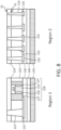
- FIG. 1 illustrates cross-sectional views of an integrated circuit device according to some embodiments of the present invention.
- the integrated circuit device may include a Region 1 and a Region 2.
- the Region 1 and the Region 2 may be spaced apart from each other in a horizontal direction (e.g., a first direction D1 and a second direction D2).
- the Region 1 may include various standard cells (e.g., logic cells).
- the standard cells may include, for example, an inverter, a 2-input NAND gate, a 3-input NAND gate, a 2-input NOR gate, a 3-input NOR gate, an And-Or inverter (AOI), an Or-And inverter (OAI), an XNOR gate, an XOR gate, a multiplexer (MUX), a latch, or a D-flip-flop.
- the Region 2 may include passive devices such as a resistor, a diode, a bipolar junction transistor, or an electrostatic discharge (ESD) protection circuit.
- the Region 1 of the integrated circuit device may include a first portion of a first structure ST1 and a first portion of a second structure ST2.
- the Region 2 of the integrated circuit device may include a second portion of the first structure ST1 and a second portion of the second structure ST2.
- the first structure ST1 and the second structure ST2 may be stacked in a vertical direction (e.g., a third direction D3).
- the first structure ST1 may include a first substrate 110.
- the horizontal direction may be parallel to one of opposing surfaces (e.g., a first surface S1 and a second surface S2 in FIG. 8 ) of the first substrate 110.
- the vertical direction may be perpendicular to one of those opposing surfaces of the first substrate 110.
- the second structure ST2 may include a second substrate 210.
- the first substrate 110 and the second substrate 210 may extend parallel to each other.
- Each of the first substrate 110 and the second substrate 210 may include one or more semiconductor materials, for example, Si, Ge, SiGe, GaP, GaAs, SiC, SiGeC and/or InP.
- each of the first substrate 110 and the second substrate 210 may be a bulk substrate (e.g., a bulk silicon substrate) or a semiconductor on insulator (SOI) substrate.
- each of the first substrate 110 and the second substrate 210 may be a silicon wafer.
- the first structure ST1 may also include a transistor 128 (e.g., a transistor of a logic cell) in the Region 1.
- the transistor 128 may include an active region 124, a gate structure 125, gate spacers 126 on opposing sides of the gate structure 125, respectively, and source/drain regions 127 adjacent to the opposing sides of the gate structure 125, respectively.
- the active region 124 may contact the first substrate 110 as illustrated in FIG. 1 , or the active region 124 may be a portion of the first substrate 110 defined by an isolation pattern (e.g., a field insulator).
- the transistor 128 may be a vertical field effect transistor (VFET) that includes source/drain regions spaced apart from each other in the vertical direction, and one of the source/drain regions may be formed in the first substrate 110.
- VFET vertical field effect transistor
- FIG. 1 illustrates the transistor 128 having a particular configuration, it should be noted that the transistor 128 may be any one of various types of transistors.
- the gate structure 125 may include a gate electrode on the active region 124 and a gate insulator extending between the active region 124 and the gate electrode.
- the gate electrode may include a semiconductor layer (e.g., a poly silicon layer), a work function layer (e.g., TiC layer, TiAl layer, TiAlC layer or TiN layer) and/or a metal layer (e.g., a tungsten layer, an aluminum layer or a copper layer), and the gate insulator may include a silicon oxide layer and/or a high-k material layer.
- the high-k material layer may include, for example, hafnium silicate, zirconium silicate, hafnium dioxide and/or zirconium dioxide.
- the gate spacers 126 may include an insulating material (e.g., silicon oxide, silicon nitride, silicon oxynitride, silicon carbide and/or a low-k material).
- the low-k material may include, for example, fluorine-doped silicon dioxide, organosilicate glass, carbon-doped oxide, porous silicon dioxide, porous organosilicate glass, spin-on organic polymeric dielectric, or spin-on silicon based polymeric dielectric.
- the source/drain regions 127 may include, for example, a semiconductor material (e.g., Si or SiGe) and/or impurities (e.g., boron, aluminum, gallium, indium, phosphorus, arsenic, antimony, bismuth and/or lithium).
- a semiconductor material e.g., Si or SiGe
- impurities e.g., boron, aluminum, gallium, indium, phosphorus, arsenic, antimony, bismuth and/or lithium.
- a first insulating layer 120 may be provided on the first substrate 110, and the transistor 128 may be provided in the first insulating layer 120.
- First, second and third contact plugs 121, 122 and 123 may also be provided in the first insulating layer 120. In some embodiments, each of the first, second and third contact plugs 121, 122 and 123 may extend through the first substrate 110 and the first insulating layer 120.
- a second insulating layer 130 may be provided on the first insulating layer 120, and first, second and third wires 131, 132 and 133 may be provided in the second insulating layer 130.
- the first, second and third wires 131, 132 and 133 may be electrically connected to the first, second and third contact plugs 121, 122 and 123, respectively.
- the first, second and third wires 131, 132 and 133 may contact the first, second and third contact plugs 121, 122 and 123, respectively.
- the first wire 131 may electrically connect the source/drain region 127 to the first contact plug 121.
- a back-end metal structure 140 may be provided on the second insulating layer 130.
- the back-end metal structure 140 may include metal vias and metal lines formed by a BEOL process. Some of the metal lines of the back-end metal structure 140 may be spaced apart from each other in the vertical direction and may be electrically connected to each other through vias. Although not illustrated, various elements (e.g., the gate electrode 125 and the first wire 131) may be electrically connected to at least one of the metal lines of the back-end metal structure 140.
- the metal vias and the metal lines of the back-end metal structure 140 may include, for example, ruthenium (Ru), cobalt (Co) and/or tungsten (W).
- the first structure ST1 may further include a first bonding insulator 160 extending on the first substrate 110 and a first etch stop layer 150 extending between the first substrate 110 and the first bonding insulator 160.
- the first etch stop layer 150 may contact the first substrate 110 and/or the first bonding insulator 160.
- opposing surfaces of the first etch stop layer 150 may contact the first substrate 110 and the first bonding insulator 160, respectively, as illustrated in FIG. 1 .
- the first structure ST1 may include a first bonding pad 161 in the Region 1 and second and third bonding pads 162 and 163 in the Region 2.
- Each of the first, second, and third bonding pads 161, 162 and 163 may extend through the first bonding insulator 160 and the first etch stop layer 150.
- the first, second and third bonding pads 161, 162 and 163 may be electrically connected to the first, second and third contact plugs 121, 122 and 123, respectively.
- the first, second and third bonding pads 161, 162 and 163 may contact the first, second and third contact plugs 121, 122 and 123, respectively.
- a width of each of the first, second and third bonding pads 161, 162 and 163 in the horizontal direction may increase as a distance from the first substrate 110 increases, as illustrated in FIG. 1 .
- the second structure ST2 may also include a passive device 216 including doped regions provided in the second substrate 210.
- the passive device 216 may be a bipolar junction transistor including three doped regions (i.e., first, second and third doped regions 213, 214 and 215) as illustrated in FIG. 1 .
- the first and third doped regions 213 and 215 may have a first conductivity type (e.g., P-type or N-type), and the second doped region 214 may have a second conductivity type that is opposite the first conductivity type.
- the first and third doped regions 213 and 215 may be P-type regions, and the second doped region 214 may be an N-type region.
- the passive device 216 may be a diode including only two doped regions that have opposite conductivity types.
- the second structure ST2 may also include a third insulating layer 220, a second etch stop layer 250 and a second bonding insulator 260 stacked on the second substrate 210.
- the second etch stop layer 250 may extend between the second bonding insulator 260 and the third insulating layer 220. In some embodiments, opposing surfaces of the second etch stop layer 250 may contact the second bonding insulator 260 and the third insulating layer 220, respectively, as illustrated in FIG. 1 .
- a resistor structure 226 may be provided in the third insulating layer 220 of the Region 2.
- the resistor structure 226 may include a resistor 225 and resistor contacts 224 that are spaced apart from each other in the horizontal direction.
- the resistor 225 may include a semiconductor material and/or metal.
- the resistor 225 may include a material the same as or different from the resistor contacts 224.
- the resistor 225 and the resistor contacts 224 may include a metal layer (e.g., a ruthenium layer, a molybdenum layer, a copper layer, a cobalt layer, an aluminum layer and/or a tungsten layer) and/or a metal nitride layer (e.g., a titanium nitride layer and/or a tantalum nitride layer).
- the resistor 225 may have a thickness in the vertical direction in a range of from about 1 nanometer (nm) to about 15 nm.
- the thickness of the resistor 225 in the vertical direction may be in a range of from about 5 nm to about 10 nm.
- the resistor 225 may be provided in the third insulating layer 220, as illustrated in FIG. 1 , or may be provided in the second substrate 210.
- the resistor 225 may include impurities (e.g., boron, aluminum, gallium, indium, phosphorus, arsenic, antimony, bismuth and/or lithium).
- the resistor contacts 224 may be provided in the third insulating layer 220, as illustrated in FIG. 1 , or may be provided in the second substrate 210.
- fourth and fifth contact plugs 221 and 222 may be provided in the third insulating layer 220, and fourth, fifth and sixth bonding pads 261, 262 and 263 may be provided in the second etch stop layer 250 and the second bonding insulator 260.
- the fourth and fifth contact plugs 221 and 222 may extend through the third insulating layer 220 and the second substrate 210 and may be electrically connected to the fourth and fifth bonding pads 261 and 262, respectively.
- the fourth and fifth contact plugs 221 and 222 may contact the fourth and fifth bonding pads 261 and 262, respectively.
- the resistor contacts 224 may be electrically connected to the sixth bonding pads 263, respectively. In some embodiments, the resistor contacts 224 may contact the sixth bonding pads 263, respectively.
- a width of each of the fourth, fifth and sixth bonding pads 261, 262 and 263 may increase as a distance from the second substrate 210 increases, as illustrated in FIG. 1 .
- the first, second and third bonding pads 161, 162 and 163 may contact the fourth, fifth and sixth bonding pads 261, 262 and 263, respectively.
- the first bonding pad 161 and the fourth bonding pad 261 may be collectively referred to as a first merged bonding pad, a width of which in the horizontal direction may increase and then decrease as a distance from the first substrate 110 increases, as illustrated in FIG. 1 .
- the second bonding pad 162 and the fifth bonding pad 262 may be collectively referred to as a second merged bonding pad, a width of which in the horizontal direction may increase and then decrease as a distance from the first substrate 110 increases.
- the third bonding pad 163 and the sixth bonding pad 263 may be collectively referred to as a third merged bonding pad, a width of which in the horizontal direction may increase and then decrease as a distance from the first substrate 110 increases.
- the integrated circuit device may include first and second power rails 311 and 312 that are provided on a surface (e.g., a fourth surface S4 in FIG. 11 ) of the second substrate 210.
- the first and second power rails 311 and 312 may be provided in a fourth insulating layer 310.
- the first and second power rails 311 and 312 and the fourth insulating layer 310 may contact the second substrate 210.
- Each of the first and second power rails 311 and 312 may extend along one of standard cell boundaries.
- one of the first and second power rails 311 and 312 may be electrically connected to multiple cells.
- the first power rail 311 may be electrically connected to source/drain regions that are included in multiple cells, respectively.
- Each of the first and second power rails 311 and 312 may be electrically connected to a first power having a first voltage (e.g., a drain voltage) or a second power having a second voltage (e.g., a source voltage).
- a power delivery network (PDN) structure 324 may be provided on the first and second power rails 311 and 312.
- the first and second power rails 311 and 312 may be provided between the second substrate 210 and the PDN structure 324 as illustrated in FIG. 1 .
- the PDN structure 324 may include a fifth insulating layer 320 and first and second power wires 321 and 322 that are provided in the fifth insulating layer 320.
- the first power wire 321 may be electrically connected to the first power rail 311. In some embodiments, the first power wire 321 may contact the first power rail 311.
- Each of the first and second etch stop layers 150 and 250 may include, for example, a silicon nitride layer and/or silicon oxynitride layer.
- the first bonding insulator 160 may include a material different from the first etch stop layer 150 such that the first bonding insulator 160 may have an etch selectivity with respect to the first etch stop layer 150.
- the second bonding insulator 260 may include a material different from the second etch stop layer 250 such that the second bonding insulator 260 may have an etch selectivity with respect to the second etch stop layer 250.
- Each of the first and second bonding insulators 160 and 260 may include, for example, a silicon oxide layer.
- Each of the first to fifth contact plugs 121, 122, 123, 221 and 222, each of the first to sixth bonding pads 161, 162, 163, 261, 262 and 263, each of the first and second power rails 311 and 312, and each of the first and second power wires 321 and 322 may be a conductor and may include a conductive material (e.g., Ru, Co and/or W).
- a conductive material e.g., Ru, Co and/or W
- Each of the first, second, third, fourth and fifth insulating layers 120, 130, 220, 310 and 320 may include an insulating material (e.g., silicon oxide, silicon oxynitride, silicon carbide and/or a low-k material).
- an insulating material e.g., silicon oxide, silicon oxynitride, silicon carbide and/or a low-k material.
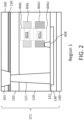
- FIG. 2 is a cross-sectional view of a first structure ST1' in a Region 1 of an integrated circuit device according to some embodiments of the present invention.
- the first structure ST1' may be similar to the first structure ST1 illustrated in FIG. 1 , with a primary difference being that the first structure ST1' includes a stacked transistor structure.
- the stacked transistor structure may include an upper transistor and a lower transistor that is provided between the first substrate 110 and the upper transistor.
- the upper transistor may include an upper active region 402U, an upper gate electrode 404U, and upper source/drain regions 406U.
- the upper source/drain regions 406U may contact opposing sides of the upper active region 402U, respectively.
- the lower transistor may include a lower active region 402L, a lower gate electrode 404L and lower source/drain regions 406L.
- the lower source/drain regions 406L may contact opposing sides of the lower active region 402L, respectively.
- the upper gate electrode 404U and the lower gate electrode 404L may be separated from each other by a gate isolation layer that is provided between the upper gate electrode 404U and the lower gate electrode 404L.
- the integrated circuit device may also include a source/drain contact 408 electrically connecting the upper source/drain region 406U to the first wire 131.
- the source/drain contact 408 may contact the upper source/drain region 406U and/or the first wire 131.
- the source/drain contact 408 may electrically connect the lower source/drain region 406L, instead of the upper source/drain region 406U, to the first wire 131.
- the upper transistor and the lower transistor may have different conductivity types.
- the upper transistor may be a P-type transistor
- the lower transistor may be an N-type transistor.
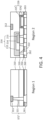
- FIG. 3 is a cross-sectional view of a second structure ST2' of an integrated circuit device according to some embodiments of the present invention.
- the second structure ST2' may be similar to the second structure ST2 illustrated in FIG. 1 , with a primary difference being that the second structure ST2' does not include the third insulating layer 220.
- the passive device 216 may contact the second etch stop layer 250, and the resistor structure 226 may be provided in the second substrate 210.
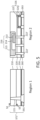
- FIG. 4 is a cross-sectional view of a second structure ST2" of an integrated circuit device according to some embodiments of the present invention.
- the second structure ST2" may be similar to the second structure ST2 in FIG. 1 , with a primary difference being that the first and second power rails 311 and 312 are provided in the second substrate 210.
- surfaces of the first and second power rails 311 and 312 may be coplanar with a surface (e.g., the fourth surface S4 in FIG. 11 ) of the second substrate 210.
- the first and second power rails 311 and 312 may be formed by forming first and second trenches in the second substrate 210 by removing portions of the second substrate 210 and then forming the first and second power rails 311 and 312 in the first and second trenches, respectively.
- the first and second trenches may be formed in the second substrate 210 by performing an etch process on the surface (e.g., the fourth surface S4 in FIG. 11 ) of the second substrate 210.
- FIG. 5 is a cross-sectional view of a second structure ST2′′′ of an integrated circuit device according to some embodiments of the present invention.
- the second structure ST2′′′ may be similar to the second structure ST2 in FIG. 1 , with primary differences being that the passive device 216 is closer to a fourth surface S4 than a third surface S3 of the second substrate 210, and portions of the fifth contact plug 222' may be provided in the second substrate 210.
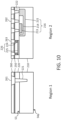
- FIG. 6 is a flow chart of methods of forming an integrated circuit device according to some embodiments of the present invention
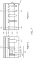
- FIGS. 7 through 12 are cross-sectional views illustrating methods of forming an integrated circuit device according to some embodiments of the present invention.
- the methods may include providing a first structure ST1 (Block 610).
- a transistor 128 may be formed on a first surface S1 of a first substrate 110 and a first insulating layer 120 may be formed around the transistor 128.
- the first insulating layer 120 may contact the first surface S1 of the first substrate 110.
- the first substrate 110 may include a preliminary second surface S2p opposite the first surface S1.
- First, second and third contact plugs 121, 122 and 123 may be formed in the first insulating layer 120.
- the first surface S1 may be referred to as an upper surface or a front side, and the preliminary second surface S2p may be referred to as a preliminary lower surface or a preliminary back side.
- the first, second and third contact plugs 121, 122 and 123 may extend through the first insulating layer 120 and may protrude into the first substrate 110.
- First, second and third wires 131, 132 and 133 may be formed on the first insulating layer 120, and a second insulating layer 130 may be formed around the first, second and third wires 131, 132 and 133.
- a back-end metal structure 140 may be formed on the second insulating layer 130 and then a carrier wafer 170 may be attached to the back-end metal structure 140.
- the carrier wafer 170 is used as a mechanical and handling support.
- the carrier wafer 170 may be made of a semiconductor material (e.g., silicon), glass and/or quartz.
- the structure shown in FIG. 7 may be turned around (e.g., flipped), and a process (e.g., a grinding process, a wet etch process and/or a dry etch process) that removes a lower portion of the first substrate 110 may be performed on the preliminary second surface S2p until the first, second and third contact plugs 121, 122 and 123 are exposed.
- a process e.g., a grinding process, a wet etch process and/or a dry etch process
- Surfaces of the first, second and third contact plugs 121, 122 and 123 may be coplanar with a second surface S2 of the first substrate 110 after removing the lower portion of the first substrate 110.
- a distance between the first surface S1 and the second surface S2 of the first substrate 110 may be in a range of 50 nm to 100 nm.
- the second surface S2 may be referred to as a lower surface or a back side.
- a first etch stop layer 150 and a first bonding insulator 160 may be sequentially formed on the second surface S2 of the first substrate 110.
- First, second and third openings, each of which may extend through the first etch stop layer 150 and the first bonding insulator 160, may be formed, and first, second and third bonding pads 161, 162 and 163 may be formed in the first, second and third openings, respectively.
- Surfaces of the first, second and third bonding pads 161, 162 and 163 may be coplanar with a surface of the first bonding insulator 160.
- the first etch stop layer 150 may include a material different from the first bonding insulator 160 to have an etch selectivity with respect to the first bonding insulator 160.
- the first, second and third openings may be formed by a two-step etch process that includes a first step etching the first bonding insulator 160 until the first etch stop layer 150 is exposed and a second step etching the first etch stop layer 150 until the first substrate 110 is exposed. The first step is stopped once the first etch stop layer 150 is exposed.
- the methods may also include providing a second structure ST2 (Block 610).
- a passive device 216 may be formed in a second substrate 210.
- First, second and third doped regions 213, 214 and 215 of the passive device 216 may be formed by implanting impurities into the second substrate 210. In some embodiments, those impurities may be implanted through a third surface S3 of the second substrate 210.
- a resistor structure 226 may be formed on the third surface S3 of the second substrate 210, and a third insulating layer 220 may be formed on the passive device 216 and the resistor structure 226.
- the second substrate 210 may include a preliminary fourth surface S4p opposite the third surface S3.
- the third surface S3 may be referred to as an upper surface or a front side, and the preliminary fourth surface S4p may be referred to as a preliminary lower surface or a preliminary back side.
- a third insulating layer 220 may be formed on the third surface S3 of the second substrate 210.
- the third insulating layer 220 may contact the third surface S3 of the second substrate 210.
- Fifth and sixth contact plugs 221 and 222 may be formed in the third insulating layer 220.
- the fifth and sixth contact plugs 221 and 222 may extend through the third insulating layer 220, and a portion of the fifth contact plug 221 may protrude into the second substrate 210.
- a second etch stop layer 250 and a second bonding insulator 260 may be sequentially formed on the third insulating layer 220.
- fourth, fifth and sixth openings each of which may extend through the second etch stop layer 250 and the second bonding insulator 260, may be formed, and then fourth, fifth and sixth bonding pads 261, 262 and 263 may be formed in the fourth, fifth and sixth openings, respectively.
- Surfaces of fourth, fifth and sixth bonding pads 261, 262 and 263 may be coplanar with a surface of the second bonding insulator 260.
- the second etch stop layer 250 may include a material different from the second bonding insulator 260 to have an etch selectivity with respect to the second bonding insulator 260.
- the fourth, fifth and sixth openings may be formed by a two-step etch process that includes a first step etching the second bonding insulator 260 until the second etch stop layer 250 is exposed and a second step etching the second etch stop layer 250 until the third insulating layer 220 is exposed. The first step is stopped once the second etch stop layer 250 is exposed.
- the structure shown in FIG. 10 may be turned around (e.g., flipped), and a process (e.g., a grinding process, a wet etch process and/or a dry etch process) that removes a lower portion of the second substrate 210 may be performed on the preliminary fourth surface S4p until the fifth contact plug 221 is exposed.
- a surface of the fifth contact plug 221 may be coplanar with a fourth surface S4 of the second substrate 210 after removing the lower portion of the second substrate 210.
- a distance between the third surface S3 and the fourth surface S4 of the second substrate 210 may be in a range of 50 nm to 100 nm. In some embodiments, the distance between the third surface S3 and the fourth surface S4 of the second substrate 210 may be longer than the distance between the first surface S1 and the second surface S2 of the first substrate 110.
- the fourth surface S4 may be referred to as a lower surface or a back side.
- the methods may also include attaching the first structure ST1 to the second structure ST2 (Block 620) using a bonding process.
- the bonding process may include an annealing process.
- the first, second and third bonding pads 161, 162 and 163 may contact the fourth, fifth and sixth bonding pads 261, 262 and 263, respectively, and the first bonding insulator 160 may contact the second bonding insulator 260, after attaching the first structure ST1 to the second structure ST2.
- first, second and third doped regions 213, 214 and 215 of the passive device 216 are formed before attaching the first structure ST1 to the second structure ST2, in some embodiments, at least one of the first, second and third doped regions 213, 214 and 215 may be formed after attaching the first structure ST1 to the second structure ST2 by implanting impurities into the second substrate 210 through the fourth surface S4 of the second substrate 210.
- the method may further include forming first and second power rails 311 and 312 on the second structure ST2 (Block 630) and forming a PDN structure 324 on the first and second power rails 311 and 312 (Block 640).
- first and second power rails 311 and 312 and a fourth insulating layer 310 may be formed on the second substrate 210.
- first and second power wires 321 and 322 and a fifth insulating layer 320 may be formed on the fourth insulating layer 310.
- the carrier wafer 170 may be removed after the PDN structure 324 is formed.
- Example embodiments of the present invention are described herein with reference to cross-sectional views that are schematic illustrations of idealized embodiments and intermediate structures of example embodiments. As such, variations from the shapes of the illustrations as a result, for example, of manufacturing techniques and/or tolerances, are to be expected. Thus, example embodiments of the present invention should not be construed as limited to the particular shapes illustrated herein but include deviations in shapes that result, for example, from manufacturing, unless the context clearly indicates otherwise.
Landscapes
- Semiconductor Integrated Circuits (AREA)
Applications Claiming Priority (2)
| Application Number | Priority Date | Filing Date | Title |
|---|---|---|---|
| US202263313763P | 2022-02-25 | 2022-02-25 | |
| US17/738,393 US12588489B2 (en) | 2022-02-25 | 2022-05-06 | Integrated circuit devices including stacked elements and methods of forming the same |
Publications (2)
| Publication Number | Publication Date |
|---|---|
| EP4235783A2 true EP4235783A2 (fr) | 2023-08-30 |
| EP4235783A3 EP4235783A3 (fr) | 2024-01-03 |
Family
ID=85321104
Family Applications (1)
| Application Number | Title | Priority Date | Filing Date |
|---|---|---|---|
| EP23157586.1A Pending EP4235783A3 (fr) | 2022-02-25 | 2023-02-20 | Dispositifs de circuit intégré comprenant des éléments empilés et leurs procédés de formation |
Country Status (4)
| Country | Link |
|---|---|
| US (1) | US12588489B2 (fr) |
| EP (1) | EP4235783A3 (fr) |
| KR (1) | KR20230127868A (fr) |
| TW (1) | TW202349631A (fr) |
Families Citing this family (2)
| Publication number | Priority date | Publication date | Assignee | Title |
|---|---|---|---|---|
| US12482746B2 (en) * | 2021-10-22 | 2025-11-25 | International Business Machines Corporation | Early backside first power delivery network |
| US12087669B1 (en) * | 2023-08-14 | 2024-09-10 | Samsung Electronics Co., Ltd. | Integrated circuit devices including discharging path and methods of forming the same |
Family Cites Families (13)
| Publication number | Priority date | Publication date | Assignee | Title |
|---|---|---|---|---|
| US8273617B2 (en) | 2009-09-30 | 2012-09-25 | Suvolta, Inc. | Electronic devices and systems, and methods for making and using the same |
| US10217667B2 (en) | 2011-06-28 | 2019-02-26 | Monolithic 3D Inc. | 3D semiconductor device, fabrication method and system |
| US20130175542A1 (en) | 2011-04-11 | 2013-07-11 | International Rectifier Corporation | Group III-V and Group IV Composite Diode |
| GB2529582B (en) | 2013-06-25 | 2019-10-23 | Intel Corp | Monolithic three-dimensional (3D) ICs with local inter-level interconnects |
| US10559594B2 (en) | 2017-04-11 | 2020-02-11 | Ahmad Tarakji | Approach to the manufacturing of monolithic 3-dimensional high-rise integrated-circuits with vertically-stacked double-sided fully-depleted silicon-on-insulator transistors |
| US10325821B1 (en) | 2017-12-13 | 2019-06-18 | International Business Machines Corporation | Three-dimensional stacked vertical transport field effect transistor logic gate with buried power bus |
| US11362189B2 (en) | 2018-09-27 | 2022-06-14 | Intel Corporation | Stacked self-aligned transistors with single workfunction metal |
| US11201148B2 (en) | 2018-10-29 | 2021-12-14 | Tokyo Electron Limited | Architecture for monolithic 3D integration of semiconductor devices |
| US20200212038A1 (en) | 2018-12-28 | 2020-07-02 | Intel Corporation | Self-aligned stacked ge/si cmos transistor structure |
| US11437376B2 (en) | 2019-05-31 | 2022-09-06 | Tokyo Electron Limited | Compact 3D stacked-CFET architecture for complex logic cells |
| US11803682B2 (en) | 2020-01-22 | 2023-10-31 | Taiwan Semiconductor Manufacturing Company Ltd. | Semiconductor device including standard cell having split portions |
| US12046567B2 (en) * | 2020-05-21 | 2024-07-23 | Taiwan Semiconductor Manufacturing Company Ltd. | Electrostatic discharge circuit and method of forming the same |
| US11581281B2 (en) * | 2020-06-26 | 2023-02-14 | Taiwan Semiconductor Manufacturing Co., Ltd. | Packaged semiconductor device and method of forming thereof |
-
2022
- 2022-05-06 US US17/738,393 patent/US12588489B2/en active Active
-
2023
- 2023-01-04 KR KR1020230001318A patent/KR20230127868A/ko active Pending
- 2023-02-20 EP EP23157586.1A patent/EP4235783A3/fr active Pending
- 2023-02-22 TW TW112106487A patent/TW202349631A/zh unknown
Also Published As
| Publication number | Publication date |
|---|---|
| KR20230127868A (ko) | 2023-09-01 |
| US12588489B2 (en) | 2026-03-24 |
| EP4235783A3 (fr) | 2024-01-03 |
| US20230275021A1 (en) | 2023-08-31 |
| TW202349631A (zh) | 2023-12-16 |
Similar Documents
| Publication | Publication Date | Title |
|---|---|---|
| CN110364507B (zh) | 半导体元件 | |
| US20210288137A1 (en) | Semiconductor device and a method of fabricating the same | |
| US7879650B2 (en) | Method of providing protection against charging damage in hybrid orientation transistors | |
| EP4235783A2 (fr) | Dispositifs de circuit intégré comprenant des éléments empilés et leurs procédés de formation | |
| EP4156271A2 (fr) | Structures de diodes de dispositifs empilés et leurs procédés de formation | |
| US12062628B2 (en) | Semiconductor device | |
| KR20230076089A (ko) | 파워 레일을 갖는 집적 회로 소자들 및 그 제조 방법 | |
| JP4340831B2 (ja) | Soi素子の基板構造及びその製造方法 | |
| US20240274598A1 (en) | Integrated circuit device and method for manufacturing the same | |
| TWI409946B (zh) | 半導體裝置及其形成方法 | |
| CN115775796B (zh) | 静电释放防护器件及其制造方法、半导体器件 | |
| US20080142861A1 (en) | Symmetric capacitor structure | |
| JP2023051808A (ja) | 半導体構造および半導体構造を製造する方法(電力レールの下でのソース/ドレイン・コンタクトの位置決め) | |
| CN116666373A (zh) | 集成电路器件及其形成方法 | |
| US20260068331A1 (en) | Vertical diode utilizing backside power delivery network | |
| US20260006875A1 (en) | Semiconductor device with backside substrate cut under the sti structure | |
| EP4723835A1 (fr) | Dispositifs de circuit intégré comprenant des transistors empilés et leurs procédés de fabrication | |
| US20240274603A1 (en) | Standard cell and ic structure with trench isolation through active regions and gate electrodes | |
| JP3254549B2 (ja) | 半導体装置及びその製造方法 | |
| CN121728832A (zh) | 半导体结构及其形成方法 | |
| CN121604402A (zh) | 电气结构及其制备方法 | |
| CN122002899A (zh) | 集成电路器件及制造集成电路器件的方法 | |
| CN120980948A (zh) | 包括场效应晶体管的半导体器件和制造该半导体器件的方法 | |
| CN120613332A (zh) | 半导体器件及其制造方法 | |
| US20040183102A1 (en) | Semiconductor antenna proximity lines |
Legal Events
| Date | Code | Title | Description |
|---|---|---|---|
| PUAI | Public reference made under article 153(3) epc to a published international application that has entered the european phase |
Free format text: ORIGINAL CODE: 0009012 |
|
| STAA | Information on the status of an ep patent application or granted ep patent |
Free format text: STATUS: THE APPLICATION HAS BEEN PUBLISHED |
|
| AK | Designated contracting states |
Kind code of ref document: A2 Designated state(s): AL AT BE BG CH CY CZ DE DK EE ES FI FR GB GR HR HU IE IS IT LI LT LU LV MC ME MK MT NL NO PL PT RO RS SE SI SK SM TR |
|
| PUAL | Search report despatched |
Free format text: ORIGINAL CODE: 0009013 |
|
| AK | Designated contracting states |
Kind code of ref document: A3 Designated state(s): AL AT BE BG CH CY CZ DE DK EE ES FI FR GB GR HR HU IE IS IT LI LT LU LV MC ME MK MT NL NO PL PT RO RS SE SI SK SM TR |
|
| RIC1 | Information provided on ipc code assigned before grant |
Ipc: H01L 21/60 20060101ALN20231124BHEP Ipc: H01L 25/18 20230101ALI20231124BHEP Ipc: H01L 25/16 20230101AFI20231124BHEP |
|
| STAA | Information on the status of an ep patent application or granted ep patent |
Free format text: STATUS: REQUEST FOR EXAMINATION WAS MADE |
|
| 17P | Request for examination filed |
Effective date: 20240625 |
|
| RBV | Designated contracting states (corrected) |
Designated state(s): AL AT BE BG CH CY CZ DE DK EE ES FI FR GB GR HR HU IE IS IT LI LT LU LV MC ME MK MT NL NO PL PT RO RS SE SI SK SM TR |