EP4235807A1 - Rückseitenmetallelektrode einer n-typ-topcon-solarzelle und herstellungsverfahren dafür sowie zelle - Google Patents
Rückseitenmetallelektrode einer n-typ-topcon-solarzelle und herstellungsverfahren dafür sowie zelle Download PDFInfo
- Publication number
- EP4235807A1 EP4235807A1 EP21912815.4A EP21912815A EP4235807A1 EP 4235807 A1 EP4235807 A1 EP 4235807A1 EP 21912815 A EP21912815 A EP 21912815A EP 4235807 A1 EP4235807 A1 EP 4235807A1
- Authority
- EP
- European Patent Office
- Prior art keywords
- silver
- grids
- aluminum
- metal electrode
- film layer
- Prior art date
- Legal status (The legal status is an assumption and is not a legal conclusion. Google has not performed a legal analysis and makes no representation as to the accuracy of the status listed.)
- Pending
Links
- 229910052751 metal Inorganic materials 0.000 title claims abstract description 48
- 239000002184 metal Substances 0.000 title claims abstract description 48
- 238000002360 preparation method Methods 0.000 title 1
- BQCADISMDOOEFD-UHFFFAOYSA-N Silver Chemical compound [Ag] BQCADISMDOOEFD-UHFFFAOYSA-N 0.000 claims abstract description 112
- 229910052709 silver Inorganic materials 0.000 claims abstract description 112
- 239000004332 silver Substances 0.000 claims abstract description 112
- 229910052782 aluminium Inorganic materials 0.000 claims abstract description 68
- XAGFODPZIPBFFR-UHFFFAOYSA-N aluminium Chemical compound [Al] XAGFODPZIPBFFR-UHFFFAOYSA-N 0.000 claims abstract description 68
- 238000007639 printing Methods 0.000 claims abstract description 24
- 238000002161 passivation Methods 0.000 claims abstract description 19
- 239000000758 substrate Substances 0.000 claims abstract description 16
- 229910004294 SiNxHy Inorganic materials 0.000 claims description 18
- 238000000034 method Methods 0.000 claims description 17
- 229910021420 polycrystalline silicon Inorganic materials 0.000 claims description 11
- VYPSYNLAJGMNEJ-UHFFFAOYSA-N Silicium dioxide Chemical compound O=[Si]=O VYPSYNLAJGMNEJ-UHFFFAOYSA-N 0.000 claims description 8
- 238000009792 diffusion process Methods 0.000 claims description 8
- 238000004518 low pressure chemical vapour deposition Methods 0.000 claims description 8
- 238000000623 plasma-assisted chemical vapour deposition Methods 0.000 claims description 8
- 229910052814 silicon oxide Inorganic materials 0.000 claims description 8
- 229910017107 AlOx Inorganic materials 0.000 claims description 7
- 239000011248 coating agent Substances 0.000 claims description 6
- 238000000576 coating method Methods 0.000 claims description 6
- 238000005245 sintering Methods 0.000 claims description 4
- 238000000151 deposition Methods 0.000 claims 2
- 239000000969 carrier Substances 0.000 abstract description 8
- 230000005540 biological transmission Effects 0.000 abstract description 7
- -1 silver-aluminum Chemical compound 0.000 abstract description 3
- 210000001503 joint Anatomy 0.000 abstract description 2
- 238000005476 soldering Methods 0.000 abstract description 2
- 238000004519 manufacturing process Methods 0.000 description 6
- 238000000231 atomic layer deposition Methods 0.000 description 4
- 230000000052 comparative effect Effects 0.000 description 4
- 238000000608 laser ablation Methods 0.000 description 4
- 229910021419 crystalline silicon Inorganic materials 0.000 description 3
- 238000006243 chemical reaction Methods 0.000 description 2
- 238000011161 development Methods 0.000 description 2
- 230000000694 effects Effects 0.000 description 2
- 238000007650 screen-printing Methods 0.000 description 2
- 230000009286 beneficial effect Effects 0.000 description 1
- 238000009826 distribution Methods 0.000 description 1
- 230000001795 light effect Effects 0.000 description 1
- 238000011056 performance test Methods 0.000 description 1
- 238000003672 processing method Methods 0.000 description 1
- 239000002994 raw material Substances 0.000 description 1
Images

Classifications
-
- H—ELECTRICITY
- H10—SEMICONDUCTOR DEVICES; ELECTRIC SOLID-STATE DEVICES NOT OTHERWISE PROVIDED FOR
- H10F—INORGANIC SEMICONDUCTOR DEVICES SENSITIVE TO INFRARED RADIATION, LIGHT, ELECTROMAGNETIC RADIATION OF SHORTER WAVELENGTH OR CORPUSCULAR RADIATION
- H10F77/00—Constructional details of devices covered by this subclass
- H10F77/20—Electrodes
- H10F77/206—Electrodes for devices having potential barriers
- H10F77/211—Electrodes for devices having potential barriers for photovoltaic cells
- H10F77/215—Geometries of grid contacts
-
- H—ELECTRICITY
- H10—SEMICONDUCTOR DEVICES; ELECTRIC SOLID-STATE DEVICES NOT OTHERWISE PROVIDED FOR
- H10F—INORGANIC SEMICONDUCTOR DEVICES SENSITIVE TO INFRARED RADIATION, LIGHT, ELECTROMAGNETIC RADIATION OF SHORTER WAVELENGTH OR CORPUSCULAR RADIATION
- H10F10/00—Individual photovoltaic cells, e.g. solar cells
- H10F10/10—Individual photovoltaic cells, e.g. solar cells having potential barriers
- H10F10/16—Photovoltaic cells having only PN heterojunction potential barriers
- H10F10/164—Photovoltaic cells having only PN heterojunction potential barriers comprising heterojunctions with Group IV materials, e.g. ITO/Si or GaAs/SiGe photovoltaic cells
- H10F10/165—Photovoltaic cells having only PN heterojunction potential barriers comprising heterojunctions with Group IV materials, e.g. ITO/Si or GaAs/SiGe photovoltaic cells the heterojunctions being Group IV-IV heterojunctions, e.g. Si/Ge, SiGe/Si or Si/SiC photovoltaic cells
-
- H—ELECTRICITY
- H10—SEMICONDUCTOR DEVICES; ELECTRIC SOLID-STATE DEVICES NOT OTHERWISE PROVIDED FOR
- H10F—INORGANIC SEMICONDUCTOR DEVICES SENSITIVE TO INFRARED RADIATION, LIGHT, ELECTROMAGNETIC RADIATION OF SHORTER WAVELENGTH OR CORPUSCULAR RADIATION
- H10F71/00—Manufacture or treatment of devices covered by this subclass
- H10F71/121—The active layers comprising only Group IV materials
-
- H—ELECTRICITY
- H10—SEMICONDUCTOR DEVICES; ELECTRIC SOLID-STATE DEVICES NOT OTHERWISE PROVIDED FOR
- H10F—INORGANIC SEMICONDUCTOR DEVICES SENSITIVE TO INFRARED RADIATION, LIGHT, ELECTROMAGNETIC RADIATION OF SHORTER WAVELENGTH OR CORPUSCULAR RADIATION
- H10F71/00—Manufacture or treatment of devices covered by this subclass
- H10F71/129—Passivating
-
- H—ELECTRICITY
- H10—SEMICONDUCTOR DEVICES; ELECTRIC SOLID-STATE DEVICES NOT OTHERWISE PROVIDED FOR
- H10F—INORGANIC SEMICONDUCTOR DEVICES SENSITIVE TO INFRARED RADIATION, LIGHT, ELECTROMAGNETIC RADIATION OF SHORTER WAVELENGTH OR CORPUSCULAR RADIATION
- H10F77/00—Constructional details of devices covered by this subclass
- H10F77/30—Coatings
- H10F77/306—Coatings for devices having potential barriers
- H10F77/311—Coatings for devices having potential barriers for photovoltaic cells
-
- H—ELECTRICITY
- H10—SEMICONDUCTOR DEVICES; ELECTRIC SOLID-STATE DEVICES NOT OTHERWISE PROVIDED FOR
- H10F—INORGANIC SEMICONDUCTOR DEVICES SENSITIVE TO INFRARED RADIATION, LIGHT, ELECTROMAGNETIC RADIATION OF SHORTER WAVELENGTH OR CORPUSCULAR RADIATION
- H10F77/00—Constructional details of devices covered by this subclass
- H10F77/30—Coatings
- H10F77/306—Coatings for devices having potential barriers
- H10F77/311—Coatings for devices having potential barriers for photovoltaic cells
- H10F77/315—Coatings for devices having potential barriers for photovoltaic cells the coatings being antireflective or having enhancing optical properties
-
- H—ELECTRICITY
- H10—SEMICONDUCTOR DEVICES; ELECTRIC SOLID-STATE DEVICES NOT OTHERWISE PROVIDED FOR
- H10F—INORGANIC SEMICONDUCTOR DEVICES SENSITIVE TO INFRARED RADIATION, LIGHT, ELECTROMAGNETIC RADIATION OF SHORTER WAVELENGTH OR CORPUSCULAR RADIATION
- H10F77/00—Constructional details of devices covered by this subclass
- H10F77/70—Surface textures, e.g. pyramid structures
- H10F77/703—Surface textures, e.g. pyramid structures of the semiconductor bodies, e.g. textured active layers
-
- Y—GENERAL TAGGING OF NEW TECHNOLOGICAL DEVELOPMENTS; GENERAL TAGGING OF CROSS-SECTIONAL TECHNOLOGIES SPANNING OVER SEVERAL SECTIONS OF THE IPC; TECHNICAL SUBJECTS COVERED BY FORMER USPC CROSS-REFERENCE ART COLLECTIONS [XRACs] AND DIGESTS
- Y02—TECHNOLOGIES OR APPLICATIONS FOR MITIGATION OR ADAPTATION AGAINST CLIMATE CHANGE
- Y02P—CLIMATE CHANGE MITIGATION TECHNOLOGIES IN THE PRODUCTION OR PROCESSING OF GOODS
- Y02P70/00—Climate change mitigation technologies in the production process for final industrial or consumer products
- Y02P70/50—Manufacturing or production processes characterised by the final manufactured product
Definitions
- the present disclosure relates to a technical field of N-type TOPCon solar cells, and specifically to a back-side metal electrode of an N-type TOPCon solar cell, a method for preparing a back-side metal electrode of N-Type TOPCon Solar Cell, and an N-type TOPCon solar cell using a back-side metal electrode as a back-side electrode.
- an N-type crystalline silicon cell is long in minority carrier lifetime, good in weak light effect and low in temperature coefficient, has no light-induced attenuation, and is the hope of crystalline silicon solar cells marching toward theoretical maximum efficiency.
- the substrate of an N-type TOPCon cell is an N-type Si wafer; a P + doped layer is obtained on the front side by means of B diffusion, and a corresponding passivation dielectric film is deposited on the front side by means of Atomic Layer Deposition (ALD) or Plasma Enhanced Chemical Vapor Deposition (PECVD); and a corresponding passivation dielectric film and an N+ doped layer are deposited on the back side by means of PECVD or Low Pressure Chemical Vapor Deposition (LPCVD).
- ALD Atomic Layer Deposition
- PECVD Plasma Enhanced Chemical Vapor Deposition
- LPCVD Low Pressure Chemical Vapor Deposition
- Corresponding metal electrodes are usually obtained on the front and back sides by means of screen printing. Silver aluminum paste is used on the front side, and silver paste is used on the back side.
- a passivation dielectric film is partially removed from the back side by means of laser ablation, then aluminum paste is printed, and a metal electrode with an ohmic contact is formed by means of sintering.
- the method requires additional device costs for laser ablation, and on the other hand, the method may damage the passivation dielectric film over a larger area, resulting in reduction of a passivation effect and reduction of electrode efficiency on the back side, thus affecting the Voc of the cell, and reducing cell efficiency.
- the line resistance of a metal grid line printed by singly using the aluminum paste is higher than that of a silver grid line, such that the FF of the cell is affected, resulting in reduction of cell efficiency.
- the present disclosure is intended to provide a back-side metal electrode of an N-type TOPCon solar cell, so as to reduce the use of silver paste on the back side, and prevent the performance of the electrode from being affected.
- Some embodiments of the present disclosure provide a method for preparing the above back-side metal electrode of an N-type TOPCon solar cell.
- Some embodiments of the present disclosure provide an N-type TOPCon solar cell using the above back-side metal electrode.
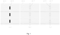
- a back-side metal electrode of an N-type TOPCon solar cell includes a substrate, and further includes a plurality of first silver fine grids disposed on a passivation film on a back side of the substrate, a plurality of second aluminum fine grids overlaid on the plurality of first silver fine grids, and a plurality of first silver main grids disposed perpendicular to the plurality of first silver fine grids, wherein each of the plurality of first silver main grids is of a segmented structure; and the back-side metal electrode further includes a plurality of second aluminum main grids, which are formed, in a printing manner, between sections of each of the plurality of the first silver main grids and around the sections.
- the plurality of first silver fine grids and the plurality of first silver main grids are printed on the passivation film; each of the plurality of first silver main grids is designed in a segmented structure; then the plurality of second aluminum fine grids are overprinted on the plurality of first silver fine grids; and the plurality of second aluminum main grids are printed on the remaining part of the plurality of first silver main grids, that is, between any two adjacent grid segments of the plurality of grid segments and around each of the plurality of grid segments, so as to make the plurality of second aluminum main grids and the plurality of first silver main grids form a partial contact channel.
- back-side carriers are collected by first passing through the plurality of first silver fine grids, then are transmitted to the plurality of second aluminum fine grids, are gathered to the plurality of second aluminum main grids, then are in contact with part of the plurality of second aluminum main grids by means of the plurality of first silver main grids, and are transferred to an external circuit by means of the plurality of first silver main grids, such that the silver paste is prevented from being excessively used on the back-side metal electrode, but is partially replaced with the aluminum paste.
- a number of the plurality of first silver fine grids is 106-122, and a width of each of the plurality of first silver fine grids is 25-40 um, and a height of the plurality of first silver fine grids is 5-10 um.
- a number of the plurality of first silver main grids is 5-12, and a number of the plurality of grid segments in each of the first silver main grids is 4-12, and a length of each of the plurality of grid segments is 2-8 mm, and a width of each of the plurality of grid segments is 0.1-2 mm, and a height of each of the plurality of grid segments is 4-8 um.
- a number of the plurality of second aluminum fine grids is 106-122, and a width of each of the plurality of second aluminum fine grids is 35-45 um, and a height of each of the plurality of second aluminum fine grids is 10-20 um.
- a number of the plurality of second aluminum main grids is 5-12, and a width of each of the plurality of second aluminum main grids is 0.3-3.0 um, and a height of each of the plurality of second aluminum main grids is 10-30 um.
- the method for preparing the above back-side metal electrode of an N-type TOPCon solar cell includes the following steps.
- the plurality of first silver fine grids are firstly printed, and the plurality of second aluminum fine grids are then overprinted, such that the transmission efficiency of metal electrode fine grids to the carriers is improved, the part of the passivation film is prevented from being removed, and the loss of the carriers is reduced.
- the plurality of first silver fine grids and the plurality of first silver main grids are simultaneously printed, such that printing efficiency is improved, and a structure where the plurality of first silver fine grids are in contact with the plurality of first silver main grids is formed.
- a transmission channel with shorter part of first silver fine grid-first silver main grid is provided at a contact part, such that the transmission efficiency of the carriers is improved.
- a thickness of the SiOx film layer is 1-8 nm; a thickness of the Poly-Si film layer is 100-200 nm; and a thickness of the back-side SiNxHy film layer is 50-100 nm.
- the present disclosure provides an N-type TOPCon solar cell using the above back-side metal electrode.
- a front side of a substrate includes a P + layer formed by means of B diffusion, a front-side anti-reflection coating consisting of an AlOx film layer deposited by means of ALD or PECVD and a front-side SiNxHy film layer deposited by means of PECVD, and a metal grid line electrode formed, in a printing manner, on the front-side anti-reflection coating.
- a thickness of the AlOx passivation film is 2-15 nm, and a thickness of the front-side SiNxHy passivation film is 50-100 nm.
- the metal grid line electrode is formed by printing and sintering silver and aluminum paste.
- a back-side metal electrode of an N-type TOPCon cell is prepared by directly using silver paste printing, and compared with a P-type PERC cell, the manufacturing cost is high, and efficiency advantages cannot be highlighted, that is, the manufacturing cost of the solar cell per watt cannot be significantly reduced.
- the back side is firstly printed with silver paste to obtain the plurality of first fine grid lines and a plurality of segmented silver main grids; and then aluminum paste overprinting is used on the plurality of first fine grid lines, so as to obtain a plurality of second fine grid lines, and the remaining a plurality of aluminum main grids are obtained on the plurality of segmented silver main grids in a printing manner.
- raw materials used in the present disclosure are commercially available or commonly used in the art; and unless otherwise specified, methods in the following embodiments are conventional in the art.
- a back-side metal electrode of an N-type TOPCon solar cell includes a substrate 1; a back side of the substrate is provided with an N+ layer by means of P diffusion; a back-side passivation film is provided on the N+ layer, and consists of an SiOx film layer 12-1, a Poly-Si film layer 12-2 and a back-side SiNxHy film layer 12-3; and the back-side passivation film is provided with a first silver fine grid 12-4, a second aluminum fine grid 12-6, a second aluminum main grid 12-7 and a first silver main grid 12-5.
- the second aluminum fine grid is prepared by overprinting aluminum paste on the first silver fine grid; the first silver fine grid is arranged perpendicular to the first silver fine grid, and include a plurality of grid segments which are disposed interval ; and the second aluminum main grid is filled and printed between any two adjacent grid segments of the plurality of grid segments and around each of the plurality of grid segments, so as to make the first silver main grids form a partial contact with the second aluminum main grids.
- the method for preparing the above back-side metal electrode of an N-type TOPCon solar cell includes the following steps:
- a front side of the substrate of the cell is formed with a P + layer 11-1 by means of B diffusion, is provided with a front-side anti-reflection coating, which including an AlOx film layer 11-2 deposited by means of ALD and a front-side SiNxHy film layer 11-3 deposited by means of PECVD.
- a thickness of the AlOx film layer is 6 nm, and a thickness of the front-side SiNxHy film layer is 70 nm.
- an H-type metal grid line electrode 11-4 is prepared by printing and sintering silver and aluminum paste on the front-side anti-reflection coating; the main grid is 9BB; and the number of fine grid is 106, with the width being 35 um and the height being 15 um.
- a back-side metal electrode of an N-type TOPCon solar cell The difference between these embodiments and the above embodiments lies in that, the number of the plurality of first silver fine grids is 122, with the width being 30 um and the height being 10 um; the number of the plurality of first silver main grids is 8, the number of the plurality of grid segments in each first silver main grid is 8, and each grid segment has a length of 8 mm, a width of 1 mm and a height of 6 um; the number of the plurality of second aluminum fine grids is 122, with the width being 35 um and the height being 15 um; and the number of the plurality of second aluminum main grids is 8, with the width being 2.0 um and the height being 15 um.
- a back-side metal electrode of an N-type TOPCon solar cell The difference between these embodiment and the above embodiments lies in that, the number of the plurality of first silver fine grids is 110, with the width being 25 um and the height being 5 um; the number of the plurality of first silver main grids is 12, the number of the plurality of grid segments in each first silver main grid is 12, and each grid segment has a length of 2mm, a width of 2mm and a height of 8 um; the number of the plurality of second aluminum fine grids is 110, with the width being 40 um and the height being 10 um; and the number of the plurality of second aluminum main grids is 12, with the width being 3.0 um and the height being 30 um.
- a back-side metal electrode of an N-type TOPCon solar cell is prepared by completely printing silver paste; and specific structure parameters are as follows: the number of silver grids is 116, with the width being 40 um and the height being 13 um; and the rest is the same as that in Embodiment 1.
- an N-type TOPCon solar cell is prepared by using the back-side metal electrode in Comparative example 1; and the remaining structures and parameters are the same as that of the N-type TOPCon solar cell in Embodiment 1.
- Embodiments 1-3 and Comparative example 1 The performance processes of the N-type TOPCon solar cell obtained in Embodiments 1-3 and Comparative example 1 are tested, and results are shown in the figures below.
- Item Short-circuit current Isc(mA/cm 2 ) Open-circuit voltage Uoc(V) Series resistance Rs(m ⁇ ) Fill factor (FF%) Conversion efficiency (Ncell%) Embodiment 1 40.66 0.706 1.7 82.27 23.62 Embodiment 2 40.66 0.702 1.4 82.72 23.61 Embodiment 3 40.66 0.700 1.2 83.02 23.63 Comparative example 1 40.66 0.706 1.9 81.97 23.54
Landscapes
- Photovoltaic Devices (AREA)
- Life Sciences & Earth Sciences (AREA)
- Sustainable Development (AREA)
Applications Claiming Priority (2)
| Application Number | Priority Date | Filing Date | Title |
|---|---|---|---|
| CN202011582094.XA CN112687755B (zh) | 2020-12-28 | 2020-12-28 | 一种N型TopCOn太阳能电池的背面金属电极及制备方法和电池 |
| PCT/CN2021/092544 WO2022142054A1 (zh) | 2020-12-28 | 2021-05-10 | 一种N型TopCOn太阳能电池的背面金属电极及制备方法和电池 |
Publications (2)
| Publication Number | Publication Date |
|---|---|
| EP4235807A1 true EP4235807A1 (de) | 2023-08-30 |
| EP4235807A4 EP4235807A4 (de) | 2024-02-21 |
Family
ID=75453480
Family Applications (1)
| Application Number | Title | Priority Date | Filing Date |
|---|---|---|---|
| EP21912815.4A Pending EP4235807A4 (de) | 2020-12-28 | 2021-05-10 | Rückseitenmetallelektrode einer n-typ-topcon-solarzelle und herstellungsverfahren dafür sowie zelle |
Country Status (5)
| Country | Link |
|---|---|
| US (1) | US12230723B2 (de) |
| EP (1) | EP4235807A4 (de) |
| CN (1) | CN112687755B (de) |
| AU (1) | AU2021415703B2 (de) |
| WO (1) | WO2022142054A1 (de) |
Families Citing this family (7)
| Publication number | Priority date | Publication date | Assignee | Title |
|---|---|---|---|---|
| CN112687755B (zh) * | 2020-12-28 | 2023-03-28 | 正泰新能科技有限公司 | 一种N型TopCOn太阳能电池的背面金属电极及制备方法和电池 |
| CN113140646B (zh) * | 2021-04-23 | 2024-05-07 | 南通天盛新能源股份有限公司 | 太阳能电池p区栅线结构及其制备方法、太阳能电池 |
| CN115763290B (zh) * | 2022-11-23 | 2026-01-23 | 广东南海启明光大科技有限公司 | 一种银铝浆搭接区域对perc电池开压影响的测试方法和装置 |
| CN116110982A (zh) * | 2023-02-08 | 2023-05-12 | 通威太阳能(眉山)有限公司 | 电池片背场结构、电池片以及光伏组件 |
| CN116457951A (zh) * | 2023-02-23 | 2023-07-18 | 深圳市首骋新材料科技有限公司 | 太阳能电池的金属化方法、太阳能电池 |
| DE102023109099A1 (de) * | 2023-04-11 | 2024-10-17 | Institut Für Solarenergieforschung Gmbh | Solarzelle mit schmalem Verbindungsbereich zwischen Kontaktfinger und Busbar |
| CN116779706A (zh) * | 2023-05-31 | 2023-09-19 | 中润新能源(滁州)有限公司 | 一种新型TOPCon电池结构及其制备工艺 |
Family Cites Families (22)
| Publication number | Priority date | Publication date | Assignee | Title |
|---|---|---|---|---|
| CN102479883A (zh) * | 2009-11-27 | 2012-05-30 | 无锡尚德太阳能电力有限公司 | 太阳电池正面电极的形成方法 |
| KR20140126313A (ko) * | 2012-01-23 | 2014-10-30 | 테트라썬, 아이엔씨. | 금속층으로부터 코팅층의 선택적인 제거, 및 그의 태양 전지 적용 |
| CN109599450A (zh) | 2013-04-03 | 2019-04-09 | Lg电子株式会社 | 太阳能电池 |
| CN105564065A (zh) | 2014-10-08 | 2016-05-11 | 上海神舟新能源发展有限公司 | N型太阳能电池二次丝网印刷方法 |
| CN106409956B (zh) * | 2016-06-27 | 2018-07-10 | 泰州隆基乐叶光伏科技有限公司 | 一种n型晶体硅双面太阳能电池结构及其制备方法 |
| CN109148616B (zh) * | 2017-06-16 | 2024-09-13 | 国家电投集团新能源科技有限公司 | 硅异质结太阳电池及其制备方法 |
| CN107331735B (zh) * | 2017-08-29 | 2018-12-28 | 浙江晶科能源有限公司 | 一种具有背面银栅线的双面perc太阳电池的制作方法 |
| CN209487520U (zh) | 2017-09-28 | 2019-10-11 | 长春永固科技有限公司 | 太阳能电池片及其组件和系统 |
| CN108365026B (zh) * | 2018-03-28 | 2024-11-08 | 通威太阳能(成都)有限公司 | 一种基于perc的双面太阳电池背面导电结构及制作方法 |
| CN208806262U (zh) * | 2018-09-29 | 2019-04-30 | 苏州腾晖光伏技术有限公司 | 一种双面晶体硅太阳能电池片 |
| CN109904249B (zh) | 2019-01-03 | 2021-08-31 | 天津爱旭太阳能科技有限公司 | P型perc双面太阳能电池背面图形对位印刷方法、制备方法及电池 |
| CN209675297U (zh) | 2019-02-25 | 2019-11-22 | 泰州隆基乐叶光伏科技有限公司 | 一种钝化接触结构及太阳能电池 |
| CN110047952A (zh) | 2019-04-04 | 2019-07-23 | 国家电投集团西安太阳能电力有限公司 | 一种太阳能电池Al栅线结构及其制备方法 |
| CN110098265A (zh) | 2019-04-29 | 2019-08-06 | 南通天盛新能源股份有限公司 | 一种n型太阳能电池正面电极金属化方法 |
| CN110165010A (zh) * | 2019-05-23 | 2019-08-23 | 江西展宇新能源股份有限公司 | 一种双面perc电池及其制备方法 |
| CN110444614A (zh) | 2019-07-31 | 2019-11-12 | 天合光能股份有限公司 | 一种N型高效TOPCon电池 |
| CN110660883A (zh) | 2019-10-09 | 2020-01-07 | 浙江正泰太阳能科技有限公司 | 一种太阳能电池的制备方法及太阳能电池 |
| CN210926031U (zh) * | 2019-11-08 | 2020-07-03 | 苏州阿特斯阳光电力科技有限公司 | 一种双面电池片、印刷电池片背面电极的网版、光伏组件 |
| CN110890432A (zh) * | 2019-11-21 | 2020-03-17 | 协鑫集成科技股份有限公司 | 一种高效多晶硅太阳能电池及其制备方法 |
| CN210866198U (zh) * | 2019-12-16 | 2020-06-26 | 苏州阿特斯阳光电力科技有限公司 | Perc双面电池及光伏组件 |
| CN111180535A (zh) * | 2020-03-05 | 2020-05-19 | 江西展宇新能科技有限公司 | 一种双面太阳能电池 |
| CN112687755B (zh) * | 2020-12-28 | 2023-03-28 | 正泰新能科技有限公司 | 一种N型TopCOn太阳能电池的背面金属电极及制备方法和电池 |
-
2020
- 2020-12-28 CN CN202011582094.XA patent/CN112687755B/zh active Active
-
2021
- 2021-05-10 WO PCT/CN2021/092544 patent/WO2022142054A1/zh not_active Ceased
- 2021-05-10 US US18/039,201 patent/US12230723B2/en active Active
- 2021-05-10 AU AU2021415703A patent/AU2021415703B2/en active Active
- 2021-05-10 EP EP21912815.4A patent/EP4235807A4/de active Pending
Also Published As
| Publication number | Publication date |
|---|---|
| WO2022142054A1 (zh) | 2022-07-07 |
| CN112687755B (zh) | 2023-03-28 |
| AU2021415703A1 (en) | 2023-06-22 |
| US20230420583A1 (en) | 2023-12-28 |
| CN112687755A (zh) | 2021-04-20 |
| EP4235807A4 (de) | 2024-02-21 |
| US12230723B2 (en) | 2025-02-18 |
| AU2021415703B2 (en) | 2024-09-19 |
Similar Documents
| Publication | Publication Date | Title |
|---|---|---|
| AU2021415703B2 (en) | Back-Side Metal Electrode of N-Type TOPCon Solar Cell, and Method for Preparing Back-Side Metal Electrode of N-Type TOPCon Solar Cell, and N-type TOPCon Solar Cell | |
| AU2021431583B2 (en) | N-type topcon cell with double-sided aluminum paste electrodes, and preparation method for preparing n-type topcon cell with double-sided aluminum paste electrodes | |
| US8883552B2 (en) | MWT architecture for thin SI solar cells | |
| KR101024288B1 (ko) | 실리콘계 박막 태양전지 | |
| US20070023082A1 (en) | Compositionally-graded back contact photovoltaic devices and methods of fabricating such devices | |
| KR101719949B1 (ko) | 태양전지 셀 및 그 제조 방법, 태양전지 모듈 | |
| US20160020342A1 (en) | Solar cell with interdigitated back contact | |
| EP3371833B1 (de) | Fotovoltaisches modul und verfahren zur herstellung davon | |
| EP2600414A1 (de) | Verfahren zur herstellung von solarzellen und solarzelle | |
| EP1279196A1 (de) | Verfahren zur herstellung einer solarzelle und nach diesem verfahren hergestellte solarzelle | |
| US20240363773A1 (en) | Solar cell, preparation method thereof and photovoltaic module | |
| US12062728B1 (en) | Solar cells | |
| EP4730369A1 (de) | Tbc-solarzelle vom p-typ und herstellungsverfahren dafür | |
| EP3206233A1 (de) | Solarzelle und verfahren zur herstellung davon | |
| CN222282014U (zh) | 一种背接触光伏电池片和光伏组件 | |
| JP5645734B2 (ja) | 太陽電池素子 | |
| CN120417557A (zh) | 太阳能电池和太阳能电池的制备方法 | |
| CN214753796U (zh) | 电池片结构及太阳能电池片和光伏组件 | |
| TWI573284B (zh) | 太陽能電池、其模組及其製造方法 | |
| KR101300803B1 (ko) | 고상성장을 이용한 태양전지 도핑층 형성방법 | |
| JP4911878B2 (ja) | 半導体/電極のコンタクト構造とこれを用いた半導体素子、太陽電池素子、並びに太陽電池モジュール | |
| CN113437161A (zh) | 太阳能电池片及其制备方法和光伏组件 | |
| US20260013262A1 (en) | Solar cell, solar cell module, and method for manufacturing solar cell | |
| JP2000068533A (ja) | 微結晶シリコン薄膜太陽電池及びその製造方法 | |
| US20110155225A1 (en) | Back contact solar cells having exposed vias |
Legal Events
| Date | Code | Title | Description |
|---|---|---|---|
| STAA | Information on the status of an ep patent application or granted ep patent |
Free format text: STATUS: THE INTERNATIONAL PUBLICATION HAS BEEN MADE |
|
| PUAI | Public reference made under article 153(3) epc to a published international application that has entered the european phase |
Free format text: ORIGINAL CODE: 0009012 |
|
| STAA | Information on the status of an ep patent application or granted ep patent |
Free format text: STATUS: REQUEST FOR EXAMINATION WAS MADE |
|
| 17P | Request for examination filed |
Effective date: 20230526 |
|
| AK | Designated contracting states |
Kind code of ref document: A1 Designated state(s): AL AT BE BG CH CY CZ DE DK EE ES FI FR GB GR HR HU IE IS IT LI LT LU LV MC MK MT NL NO PL PT RO RS SE SI SK SM TR |
|
| REG | Reference to a national code |
Ref country code: DE Ref legal event code: R079 Free format text: PREVIOUS MAIN CLASS: H01L0031022400 Ipc: H01L0031074500 |
|
| A4 | Supplementary search report drawn up and despatched |
Effective date: 20240123 |
|
| RIC1 | Information provided on ipc code assigned before grant |
Ipc: H01L 31/18 20060101ALI20240117BHEP Ipc: H01L 31/0224 20060101ALI20240117BHEP Ipc: H01L 31/0216 20140101ALI20240117BHEP Ipc: H01L 31/0745 20120101AFI20240117BHEP |
|
| DAV | Request for validation of the european patent (deleted) | ||
| DAX | Request for extension of the european patent (deleted) |