EP4235957A1 - Elektrische vorrichtung und deren hochfrequenzübertragungsleitung - Google Patents
Elektrische vorrichtung und deren hochfrequenzübertragungsleitung Download PDFInfo
- Publication number
- EP4235957A1 EP4235957A1 EP22181317.3A EP22181317A EP4235957A1 EP 4235957 A1 EP4235957 A1 EP 4235957A1 EP 22181317 A EP22181317 A EP 22181317A EP 4235957 A1 EP4235957 A1 EP 4235957A1
- Authority
- EP
- European Patent Office
- Prior art keywords
- band
- shaped line
- line segment
- segment
- coplanar waveguide
- Prior art date
- Legal status (The legal status is an assumption and is not a legal conclusion. Google has not performed a legal analysis and makes no representation as to the accuracy of the status listed.)
- Pending
Links
Images


Classifications
-
- H—ELECTRICITY
- H01—ELECTRIC ELEMENTS
- H01P—WAVEGUIDES; RESONATORS, LINES, OR OTHER DEVICES OF THE WAVEGUIDE TYPE
- H01P3/00—Waveguides; Transmission lines of the waveguide type
- H01P3/02—Waveguides; Transmission lines of the waveguide type with two longitudinal conductors
- H01P3/08—Microstrips; Strip lines
- H01P3/085—Triplate lines
-
- H—ELECTRICITY
- H01—ELECTRIC ELEMENTS
- H01P—WAVEGUIDES; RESONATORS, LINES, OR OTHER DEVICES OF THE WAVEGUIDE TYPE
- H01P5/00—Coupling devices of the waveguide type
- H01P5/02—Coupling devices of the waveguide type with invariable factor of coupling
- H01P5/022—Transitions between lines of the same kind and shape, but with different dimensions
- H01P5/028—Transitions between lines of the same kind and shape, but with different dimensions between strip lines
-
- H—ELECTRICITY
- H01—ELECTRIC ELEMENTS
- H01P—WAVEGUIDES; RESONATORS, LINES, OR OTHER DEVICES OF THE WAVEGUIDE TYPE
- H01P3/00—Waveguides; Transmission lines of the waveguide type
- H01P3/02—Waveguides; Transmission lines of the waveguide type with two longitudinal conductors
- H01P3/08—Microstrips; Strip lines
-
- H—ELECTRICITY
- H01—ELECTRIC ELEMENTS
- H01P—WAVEGUIDES; RESONATORS, LINES, OR OTHER DEVICES OF THE WAVEGUIDE TYPE
- H01P1/00—Auxiliary devices
- H01P1/06—Movable joints, e.g. rotating joints
- H01P1/062—Movable joints, e.g. rotating joints the relative movement being a rotation
- H01P1/063—Movable joints, e.g. rotating joints the relative movement being a rotation with a limited angle of rotation
- H01P1/064—Movable joints, e.g. rotating joints the relative movement being a rotation with a limited angle of rotation the axis of rotation being perpendicular to the transmission path, e.g. hinge joint
-
- H—ELECTRICITY
- H01—ELECTRIC ELEMENTS
- H01P—WAVEGUIDES; RESONATORS, LINES, OR OTHER DEVICES OF THE WAVEGUIDE TYPE
- H01P3/00—Waveguides; Transmission lines of the waveguide type
- H01P3/003—Coplanar lines
-
- H—ELECTRICITY
- H01—ELECTRIC ELEMENTS
- H01P—WAVEGUIDES; RESONATORS, LINES, OR OTHER DEVICES OF THE WAVEGUIDE TYPE
- H01P3/00—Waveguides; Transmission lines of the waveguide type
- H01P3/003—Coplanar lines
- H01P3/006—Conductor backed coplanar waveguides
-
- H—ELECTRICITY
- H01—ELECTRIC ELEMENTS
- H01P—WAVEGUIDES; RESONATORS, LINES, OR OTHER DEVICES OF THE WAVEGUIDE TYPE
- H01P3/00—Waveguides; Transmission lines of the waveguide type
- H01P3/02—Waveguides; Transmission lines of the waveguide type with two longitudinal conductors
- H01P3/026—Coplanar striplines [CPS]
-
- H—ELECTRICITY
- H01—ELECTRIC ELEMENTS
- H01P—WAVEGUIDES; RESONATORS, LINES, OR OTHER DEVICES OF THE WAVEGUIDE TYPE
- H01P5/00—Coupling devices of the waveguide type
- H01P5/08—Coupling devices of the waveguide type for linking dissimilar lines or devices
-
- H—ELECTRICITY
- H05—ELECTRIC TECHNIQUES NOT OTHERWISE PROVIDED FOR
- H05K—PRINTED CIRCUITS; CASINGS OR CONSTRUCTIONAL DETAILS OF ELECTRIC APPARATUS; MANUFACTURE OF ASSEMBLAGES OF ELECTRICAL COMPONENTS
- H05K1/00—Printed circuits
- H05K1/02—Details
- H05K1/14—Structural association of two or more printed circuits
- H05K1/148—Arrangements of two or more hingeably connected rigid printed circuit boards, i.e. connected by flexible means
-
- H—ELECTRICITY
- H05—ELECTRIC TECHNIQUES NOT OTHERWISE PROVIDED FOR
- H05K—PRINTED CIRCUITS; CASINGS OR CONSTRUCTIONAL DETAILS OF ELECTRIC APPARATUS; MANUFACTURE OF ASSEMBLAGES OF ELECTRICAL COMPONENTS
- H05K1/00—Printed circuits
- H05K1/18—Printed circuits structurally associated with non-printed electric components
-
- H—ELECTRICITY
- H05—ELECTRIC TECHNIQUES NOT OTHERWISE PROVIDED FOR
- H05K—PRINTED CIRCUITS; CASINGS OR CONSTRUCTIONAL DETAILS OF ELECTRIC APPARATUS; MANUFACTURE OF ASSEMBLAGES OF ELECTRICAL COMPONENTS
- H05K2201/00—Indexing scheme relating to printed circuits covered by H05K1/00
- H05K2201/10—Details of components or other objects attached to or integrated in a printed circuit board
- H05K2201/10007—Types of components
- H05K2201/10189—Non-printed connector
-
- Y—GENERAL TAGGING OF NEW TECHNOLOGICAL DEVELOPMENTS; GENERAL TAGGING OF CROSS-SECTIONAL TECHNOLOGIES SPANNING OVER SEVERAL SECTIONS OF THE IPC; TECHNICAL SUBJECTS COVERED BY FORMER USPC CROSS-REFERENCE ART COLLECTIONS [XRACs] AND DIGESTS
- Y02—TECHNOLOGIES OR APPLICATIONS FOR MITIGATION OR ADAPTATION AGAINST CLIMATE CHANGE
- Y02D—CLIMATE CHANGE MITIGATION TECHNOLOGIES IN INFORMATION AND COMMUNICATION TECHNOLOGIES [ICT], I.E. INFORMATION AND COMMUNICATION TECHNOLOGIES AIMING AT THE REDUCTION OF THEIR OWN ENERGY USE
- Y02D30/00—Reducing energy consumption in communication networks
- Y02D30/70—Reducing energy consumption in communication networks in wireless communication networks
Definitions
- the present invention relates to a field of electronic devices, and more particularly to an electronic device and its radio-frequency transmission line.
- Antennas of electronic devices that cannot be folded are arranged as metal frames around the electronic devices.
- a pivot shaft is arranged at a side of the electronic device in a folded state.
- the present invention seeks to solve at least one of the problems existing in the related art to at least some extent.
- embodiments of the present invention propose an electronic device and its radio-frequency transmission line.
- the electronic device includes a first body and a second body rotatably connected relative to each other through a pivot shaft, the first body including a first motherboard, the second body including a second motherboard; and a radio-frequency transmission line having a first end coupled to the first motherboard and a second end coupled to the second motherboard, the radio-frequency transmission line including at least one band-shaped line segment and at least two coplanar waveguide segments, the band-shaped line segment being coupled to the coplanar waveguide segments, in which one band-shaped line segment is located between two coplanar waveguide segments in an extending direction of the radio-frequency transmission line, one band-shaped line segment is coupled to the pivot shaft to retain stationary relative to the pivot shaft, and the coplanar waveguide segments are spaced apart from a metal portion of the pivot shaft.
- the electronic device has advantages of continuous impedance after several bends of the radio-frequency transmission line and high signal transmission quality after bending of the radio-frequency transmission line.
- the radio-frequency transmission line includes 2N+1 band-shaped line segments and 2N coplanar waveguide segments arranged alternately and connected sequentially in the extending direction, in which N is an integer greater than or equal to 1, each coplanar waveguide segment is located between two adjacent band-shaped line segments in the extending direction, one of a plurality of band-shaped line segments is coupled to the first motherboard, and another of the plurality of band-shaped line segments is coupled to the second motherboard.
- the band-shaped line segments include a first band-shaped line segment, a second band-shaped line segment and a third band-shaped line segment arranged sequentially in the extending direction, the first band-shaped line segment is coupled to the first motherboard, the third band-shaped line segment is coupled to the second motherboard, and the second band-shaped line segment is coupled to the pivot shaft to retain stationary relative to the pivot shaft, in which the pivot shaft is located between the first band-shaped line segment and the third band-shaped line segment in the extending direction;
- the coplanar waveguide segments include a first coplanar waveguide segment located between the first band-shaped line segment and the second band-shaped line segment in the extending direction, the first coplanar waveguide segment being coupled to each of the first band-shaped line segment and the second band-shaped line segment; and a second coplanar waveguide segment located between the second band-shaped line segment and the third band-shaped line segment in the extending direction, the second coplanar waveguide segment being coupled to each of the second band-shaped line segment and the third band-shaped line segment, the first coplanar waveguide segment and the second coplanar waveguide segment are spaced apart from the metal portion of the pivot shaft.
- each of the first coplanar waveguide segment and the second coplanar waveguide segment has a length less than or equal to a first preset value.
- the band-shaped line segments include a first band-shaped line segment, a second band-shaped line segment, a third band-shaped line segment, a fourth band-shaped line segment and a fifth band-shaped line segment arranged sequentially in the extending direction, the first band-shaped line segment is coupled to the first motherboard, the fifth band-shaped line segment is coupled to the second motherboard, and the third band-shaped line segment is coupled to the pivot shaft to retain stationary relative to the pivot shaft, in which the pivot shaft is located between the first band-shaped line segment and the fifth band-shaped line segment in the extending direction;
- the coplanar waveguide segments include a first coplanar waveguide segment located between the first band-shaped line segment and the second band-shaped line segment in the extending direction, the first coplanar waveguide segment being coupled to each of the first band-shaped line segment and the second band-shaped line segment; a second coplanar waveguide segment located between the second band-shaped line segment and the third band-shaped line segment in the extending direction, the second coplanar waveguide segment being coupled to each of the second band-shaped line segment and the third band-shaped line segment; a third coplanar waveguide segment located between the third band-shaped line segment and the fourth band-shaped line segment in the extending direction, the third coplanar waveguide segment being coupled to each of the third band-shaped line segment and the fourth band-shaped line segment; and a fourth coplanar waveguide segment located between the fourth band-shaped line segment and the fifth band-shaped line segment in the extending direction, the fourth coplanar waveguide segment being coupled to each of the fourth band-shaped line segment and the fifth band-shaped line segment, in
- each of the first coplanar waveguide segment, the second coplanar waveguide segment, the third coplanar waveguide segment and the fourth coplanar waveguide segment has a length greater than or equal to a second preset value and less than or equal to a third preset value.
- each of the second band-shaped line segment and the fourth band-shaped line segment has a length less than or equal to a fourth preset value.
- each coplanar waveguide segment has a metal trace layer including a base part, each base part having a width greater than a width of the metal trace layer of the band-shaped line segment; a first transition part having a first end part coupled to the metal trace layer of a corresponding band-shaped line segment and a second end part coupled to the base part, in which the first end part of the first transition part has a width equal to the width of the metal trace layer of the corresponding band-shaped line segment, the second end part of the first transition part has a width equal to the width of the base part, the first transition part has a width increasing in the extending direction and along a direction towards the base part; and a second transition part having a first end part coupled to the metal trace layer of a corresponding band-shaped line segment and a second end part coupled to the base part, the base part being located between the first transition part and the second transition part in the extending direction, in which the first end part of the second transition part has a width equal to the width of the metal trace layer of the corresponding
- the width of the first transition part increases gradually in the extending direction and along the direction towards the base part; and the width of the second transition part decreases gradually in the extending direction and along the direction away from the base part.
- the radio-frequency transmission line includes a first metal ground assembly including a first modified polyimide layer and a first metal ground layer arranged on the first modified polyimide layer; a second metal ground assembly including a second modified polyimide layer and a second metal ground layer arranged on the second modified polyimide layer; and a metal trace assembly including a third modified polyimide layer and a metal trace layer arranged on the third modified polyimide layer, the first metal ground layer, the first modified polyimide layer, the metal trace layer, the third modified polyimide layer, the second metal ground layer and the second modified polyimide layer being arranged sequentially in a thickness direction of the radio-frequency transmission line, in which the first metal ground layer has a first through hole therethrough in the thickness direction, the second metal ground layer has a second through hole therethrough in the thickness direction, the first through hole and the second through hole are opposite in the thickness direction, a portion of the radio-frequency transmission line opposite the first through hole in the thickness direction constitutes the coplanar waveguide segment, and the band-shaped line
- the radio-frequency transmission line includes: at least one band-shaped line segment and at least two coplanar waveguide segments, one band-shaped line segment is located between two coplanar waveguide segments in an extending direction of the radio-frequency transmission line, the band-shaped line segment being coupled to the coplanar waveguide segments.
- the radio-frequency transmission line according to embodiments of the present invention has advantages of continuous impedance after several bends and high signal transmission quality after bending.
- the radio-frequency transmission line includes 2N+1 band-shaped line segments and 2N coplanar waveguide segments arranged alternately and connected sequentially in the extending direction, in which N is an integer greater than or equal to 1, each coplanar waveguide segment is located between two adjacent band-shaped line segments in the extending direction.
- the band-shaped line segments include a first band-shaped line segment, a second band-shaped line segment and a third band-shaped line segment arranged sequentially in the extending direction;
- the coplanar waveguide segments include a first coplanar waveguide segment located between the first band-shaped line segment and the second band-shaped line segment in the extending direction, the first coplanar waveguide segment being coupled to each of the first band-shaped line segment and the second band-shaped line segment; and a second coplanar waveguide segment located between the second band-shaped line segment and the third band-shaped line segment in the extending direction, the second coplanar waveguide segment being coupled to each of the second band-shaped line segment and the third band-shaped line segment.
- each of the first coplanar waveguide segment and the second coplanar waveguide segment has a length less than or equal to a first preset value.
- the band-shaped line segments include a first band-shaped line segment, a second band-shaped line segment, a third band-shaped line segment, a fourth band-shaped line segment and a fifth band-shaped line segment arranged sequentially in the extending direction;
- the coplanar waveguide segments include a first coplanar waveguide segment located between the first band-shaped line segment and the second band-shaped line segment in the extending direction, the first coplanar waveguide segment being coupled to each of the first band-shaped line segment and the second band-shaped line segment; a second coplanar waveguide segment located between the second band-shaped line segment and the third band-shaped line segment in the extending direction, the second coplanar waveguide segment being coupled to each of the second band-shaped line segment and the third band-shaped line segment; a third coplanar waveguide segment located between the third band-shaped line segment and the fourth band-shaped line segment in the extending direction, the third coplanar waveguide segment being coupled to each of the third band-shaped line segment and the fourth band-shaped line segment;
- each of the first coplanar waveguide segment, the second coplanar waveguide segment, the third coplanar waveguide segment and the fourth coplanar waveguide segment has a length greater than or equal to a second preset value and less than or equal to a third preset value.
- each of the second band-shaped line segment and the fourth band-shaped line segment has a length less than or equal to a fourth preset value.
- each coplanar waveguide segment has a metal trace layer including: a base part, each base part having a width greater than a width of the metal trace layer of the band-shaped line segment; a first transition part having a first end part coupled to the metal trace layer of a corresponding band-shaped line segment and a second end part coupled to the base part, in which the first end part of the first transition part has a width equal to the width of the metal trace layer of the corresponding band-shaped line segment, the second end part of the first transition part has a width equal to the width of the base part, the first transition part has a width increasing in the extending direction and along a direction towards the base part; and a second transition part having a first end part coupled to the metal trace layer of a corresponding band-shaped line segment and a second end part coupled to the base part, the base part being located between the first transition part and the second transition part in the extending direction, in which the first end part of the second transition part has a width equal to the width of the metal trace layer of the
- the width of the first transition part increases gradually in the extending direction and along the direction towards the base part; and the width of the second transition part decreases gradually in the extending direction and along the direction away from the base part.
- the radio-frequency transmission line includes a first metal ground assembly including a first modified polyimide layer and a first metal ground layer arranged on the first modified polyimide layer; a second metal ground assembly including a second modified polyimide layer and a second metal ground layer arranged on the second modified polyimide layer; and a metal trace assembly including a third modified polyimide layer and a metal trace layer arranged on the third modified polyimide layer, the first metal ground layer, the first modified polyimide layer, the metal trace layer, the third modified polyimide layer, the second metal ground layer and the second modified polyimide layer being arranged sequentially in a thickness direction of the radio-frequency transmission line, in which the first metal ground layer has a first through hole therethrough in the thickness direction, the second metal ground layer has a second through hole therethrough in the thickness direction, the first through hole and the second through hole are opposite in the thickness direction, a portion of the radio-frequency transmission line opposite the first through hole in the thickness direction constitutes the coplanar waveguide segment, and the band-shaped line
- a pivot shaft is arranged at a side of the electronic device in a folded state, thus antennas can only be arranged at the other three sides of the electronic device in the folded state.
- Such an antenna arrangement cannot meet the needs of multiple frequency bands.
- the electronic device 100 includes a first body 21, a second body 22, and a radio-frequency transmission line 1.
- the first body 21 and the second body 22 are rotatably connected relative to each other through a pivot shaft 4. That is, the first body 21 and the second body 22 are pivotally connected through the pivot shaft 4. That is to say, it is possible to keep the first body 21 still and rotate the second body 22, it is also possible to keep the second body 22 still and rotate the first body 21, and it is further possible to rotate both the first body 21 and the second body 22.
- the first body 21 includes a first motherboard 211
- the second body 22 includes a second motherboard 221.
- a first end of the radio-frequency transmission line 1 is coupled to the first motherboard 211, and a second end of the radio-frequency transmission line 1 is coupled to the second motherboard 221.
- the radio-frequency transmission line 1 includes at least one band-shaped line segment 11 and at least two coplanar waveguide segments 12, and the band-shaped line segment 11 is coupled to the coplanar waveguide segments 12.
- One band-shaped line segment 11 is located between two coplanar waveguide segments 12 in an extending direction of the radio-frequency transmission line 1.
- One band-shaped line segment 11 is coupled to the pivot shaft 4 to retain stationary relative to the pivot shaft 4.
- the one band-shaped line segment 11 may be adhered to the pivot shaft 4, or the one band-shaped line segment 11 may be coupled to the pivot shaft 4 through a snap or a snapping slot.
- the coplanar waveguide segments 12 are spaced apart from a metal portion of the pivot shaft 4.
- the radio-frequency transmission line 1 When at least one of the first body 21 and the second body 22 is rotated, the radio-frequency transmission line 1 is bent. If the whole radio-frequency transmission line employs a band-shaped line structure, a metal ground layer of the radio-frequency transmission line will break after several bends, resulting in discontinuous impedance of the radio-frequency transmission line. If the whole radio-frequency transmission line employs a coplanar waveguide structure, a portion of the radio-frequency transmission line is covered by the metal portion of the pivot shaft, resulting in discontinuous impedance of the radio-frequency transmission line.
- one band-shaped line segment 11 of the radio-frequency transmission line 1 is coupled to the pivot shaft 4, and hence the one band-shaped line segment 11 may be retained stationary relative to the pivot shaft 4.
- the one band-shaped line segment 11 will not bend, to prevent a metal ground layer of the one band-shaped line segment 11 from breaking after several bends and further avoid discontinuous impedance of the band-shaped line segment 11.
- the coplanar waveguide segments 12 are spaced apart from the metal portion of the pivot shaft 4, thus the coplanar waveguide segments 12 may be prevented from being covered by the metal portion of the pivot shaft 4, to avoid discontinuous of the coplanar waveguide segments 12.
- the coplanar waveguide segment 12 may not be opposite to the metal portion of the pivot shaft 4, to be spaced apart from the metal portion of the pivot shaft 4.
- a spacer layer e.g., a foam layer
- the coplanar waveguide segment 12 is spaced apart from the metal portion of the pivot shaft 4.
- the radio-frequency transmission line 1 has advantages of continuous impedance after several bends, high signal transmission quality after bending and the like, and can apply to foldable electronic devices.
- the electronic device 100 according to embodiments of the present invention has advantages of continuous impedance after several bends of the radio-frequency transmission line, high signal transmission quality after bending of the radio-frequency transmission line and the like.
- the first body 21 includes a first motherboard 211
- the second body 22 includes a second motherboard 221.
- a first end of the radio-frequency transmission line 1 is coupled to the first motherboard 211
- a second end of the radio-frequency transmission line 1 is coupled to the second motherboard 221.
- the radio-frequency transmission line 1 includes 2N+1 band-shaped line segments 11 and 2N coplanar waveguide segments 12.
- the 2N+1 band-shaped line segments 11 and the 2N coplanar waveguide segments 12 are alternately arranged in the extending direction of the radio-frequency transmission line 1.
- the 2N+1 band-shaped line segments 11 and the 2N coplanar waveguide segments 12 are connected sequentially.
- the extending direction of the radio-frequency transmission line 1 is represented by an arrow A in FIG. 5 .
- the radio-frequency transmission line 1 includes the 2N+1 band-shaped line segments 11 and the 2N coplanar waveguide segments 12, thus lengths of each band-shaped line segment 11 and each coplanar waveguide segment 12 may be controlled more conveniently and more effectively, to make structures of the radio-frequency transmission line 1 and the electronic device 100 more reasonable.
- each coplanar waveguide segment 12 is located between two adjacent band-shaped line segments 11 in the extending direction of the radio-frequency transmission line 1.
- one of the band-shaped line segments 11 may be coupled to the first motherboard 211, and another of the band-shaped line segments 11 may be coupled to the second motherboard 221.
- the radio-frequency transmission line 1 may be coupled to the first motherboard 211 and the second motherboard 221 more conveniently and more easily.
- one of the band-shaped line segments 11 is coupled to the first motherboard 211 through a first BTB (board-to-board) connector 31, and another of the band-shaped line segments 11 may be coupled to the second motherboard 221 through a second BTB connector 32.
- the band-shaped line segments 11 includes a first band-shaped line segment 11a, a second band-shaped line segment 11b and a third band-shaped line segment 11c arranged sequentially in the extending direction of the radio-frequency transmission line 1.
- the first band-shaped line segment 11a is coupled to the first motherboard 211
- the third band-shaped line segment 11c is coupled to the second motherboard 221.
- the first band-shaped line segments 11a is coupled to the first motherboard 211 through the first BTB connector 31
- the third band-shaped line segments 11c is coupled to the second motherboard 221 through the second BTB connector 32.
- the second band-shaped line segment 11b is coupled to the pivot shaft 4 to stay stationary relative to the pivot shaft 4.
- the pivot shaft 4 is located between the first band-shaped line segment 11a and the third band-shaped line segment 11c in the extending direction of the radio-frequency transmission line 1. That is to say, the first band-shaped line segment 11a and the third band-shaped line segment 11c are located outside the pivot shaft 4.
- the coplanar waveguide segments 12 include a first coplanar waveguide segment 12a and a second coplanar waveguide segment 12b.
- the first coplanar waveguide segment 12a is located between the first band-shaped line segment 11a and the second band-shaped line segment 11b in the extending direction of the radio-frequency transmission line 1, and the first coplanar waveguide segment 12a is coupled to each of the first band-shaped line segment 11a and the second band-shaped line segment 11b.
- the second coplanar waveguide segment 12b is located between the second band-shaped line segment 11b and the third band-shaped line segment 11c in the extending direction of the radio-frequency transmission line 1, and the second coplanar waveguide segment 12b is coupled to each of the second band-shaped line segment 11b and the third band-shaped line segment 11c.
- the second band-shaped line segment 11b is located between the first coplanar waveguide segment 12a and the second coplanar waveguide segment 12b in the extending direction of the radio-frequency transmission line 1, and the second band-shaped line segment 11b is coupled to each of the first coplanar waveguide segment 12a and the second coplanar waveguide segment 12b.
- the first coplanar waveguide segment 12a and the second coplanar waveguide segment 12b are spaced apart from the metal portion of the pivot shaft 4. Thus, the first coplanar waveguide segment 12a and the second coplanar waveguide segment 12b may be prevented from being covered by the metal portion of the pivot shaft 4, to avoid discontinuous impedance of the first coplanar waveguide segment 12a and the second coplanar waveguide segment 12b, and further avoid the discontinuous impedance of the radio-frequency transmission line 1.
- each of the first coplanar waveguide segment 12a and the second coplanar waveguide segment 12b has a length less than or equal to a first preset value.
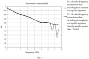
- the radio-frequency transmission line 1 and the electronic device 100 may have no noise wave below 7.5GHz, i.e., they will not generate resonance point below 7.5GH, to reduce loss of the radio-frequency transmission line 1 and the electronic device 100.
- each of the first coplanar waveguide segment 12a and the second coplanar waveguide segment 12b has a length less than or equal to 12 millimeters.
- the radio-frequency transmission line 1 and the electronic device 100 may be further ensured to have no noise wave below 7.5GHz, i.e., they are further ensured not to generate resonance point below 7.5GH, to further reduce loss of the radio-frequency transmission line 1 and the electronic device 100.
- each of the first coplanar waveguide segment 12a and the second coplanar waveguide segment 12b has a length less than or equal to 11 millimeters.
- the radio-frequency transmission line 1 and the electronic device 100 may be further ensured to have no noise wave below 7.5GHz, i.e., they are further ensured not to generate resonance point below 7.5GH, to further reduce loss of the radio-frequency transmission line 1 and the electronic device 100.
- each of the first coplanar waveguide segment 12a and the second coplanar waveguide segment 12b has a length less than or equal to 10 millimeters.
- the radio-frequency transmission line 1 and the electronic device 100 may be further ensured to have no noise wave below 7.5GHz, i.e., they are further ensured not to generate resonance point below 7.5GH, to further reduce loss of the radio-frequency transmission line 1 and the electronic device 100.
- each of the first coplanar waveguide segment 12a and the second coplanar waveguide segment 12b has a length less than or equal to 8 millimeters.
- the radio-frequency transmission line 1 and the electronic device 100 may be further ensured to have no noise wave below 7.5GHz, i.e., they are further ensured not to generate resonance point below 7.5GH, to further reduce loss of the radio-frequency transmission line 1 and the electronic device 100.
- the length of each of the first coplanar waveguide segment 12a and the second coplanar waveguide segment 12b may be 5 millimeters, 5.5 millimeters, 6 millimeters, 6.5 millimeters, 7 millimeters, 7.5 millimeters, 8 millimeters, 8.5 millimeters, 9 millimeters, 9.5 millimeters, 10 millimeters, 10.5 millimeters, 11 millimeters, 11.5 millimeters or 12 millimeters.
- lengths of the first coplanar waveguide segment 12a and the second coplanar waveguide segment 12b may be equal to each other.
- the radio-frequency transmission line 1 and the electronic device 100 may have more reasonable structures.
- Lengths of the first band-shaped line segment 11a and the third band-shaped line segment 11c may be equal to each other.
- the radio-frequency transmission line 1 and the electronic device 100 may have more reasonable structures.
- the band-shaped line segments 11 include a first band-shaped line segment 11a, a second band-shaped line segment 11b, a third band-shaped line segment 11c, a fourth band-shaped line segment 11d and a fifth band-shaped line segment 11e arranged sequentially in the extending direction of the radio-frequency transmission line 1.
- the first band-shaped line segment 11a is coupled to the first motherboard 211
- the fifth band-shaped line segment 11e is coupled to the second motherboard 221.
- the first band-shaped line segment 11a is coupled to the first motherboard 211 through the first BTB connector 31
- the fifth band-shaped line segment 11e is coupled to the second motherboard 221 through the second BTB connector 32.
- the third band-shaped line segment 11c is coupled to the pivot shaft 4 to stay stationary relative to the pivot shaft 4.
- the pivot shaft 4 is located between the first band-shaped line segment 11a and the fifth band-shaped line segment 11e in the extending direction of the radio-frequency transmission line 1. That is to say, the first band-shaped line segment 11a and the fifth band-shaped line segment 11e are located outside the pivot shaft 4.
- the coplanar waveguide segments include a first coplanar waveguide segment 12a, a second coplanar waveguide segment 12b, a third coplanar waveguide segment 12c, and a fourth coplanar waveguide segment 12d.
- the first coplanar waveguide segment 12a is located between the first band-shaped line segment 11a and the second band-shaped line segment 11b in the extending direction of the radio-frequency transmission line 1, and the first coplanar waveguide segment 12a is coupled to each of the first band-shaped line segment 11a and the second band-shaped line segment 11b.
- the second coplanar waveguide segment 12b is located between the second band-shaped line segment 11b and the third band-shaped line segment 11c in the extending direction of the radio-frequency transmission line 1, and the second coplanar waveguide segment 12b is coupled to each of the second band-shaped line segment 11b and the third band-shaped line segment 11c.
- the third coplanar waveguide segment 12c is located between the third band-shaped line segment 11c and the fourth band-shaped line segment 11d in the extending direction of the radio-frequency transmission line 1, and the third coplanar waveguide segment 12c is coupled to each of the third band-shaped line segment 11c and the fourth band-shaped line segment 11d.
- the fourth coplanar waveguide segment 12d is located between the fourth band-shaped line segment 11d and the fifth band-shaped line segment 11e in the extending direction of the radio-frequency transmission line 1, and the fourth coplanar waveguide segment 12d is coupled to each of the fourth band-shaped line segment 11d and the fifth band-shaped line segment 11e.
- the radio-frequency transmission line 1 includes the first band-shaped line segment 11a, the first coplanar waveguide segment 12a, the second band-shaped line segment 11b, the second coplanar waveguide segment 12b, the third band-shaped line segment 11c, the third coplanar waveguide segment 12c, the fourth band-shaped line segment 11d, the fourth coplanar waveguide segment 12d and the fifth band-shaped line segment 11e arranged sequentially in the extending direction.
- the first band-shaped line segment 11a, the first coplanar waveguide segment 12a, the second band-shaped line segment 11b, the second coplanar waveguide segment 12b, the third band-shaped line segment 11c, the third coplanar waveguide segment 12c, the fourth band-shaped line segment 11d, the fourth coplanar waveguide segment 12d and the fifth band-shaped line segment 11e are connected sequentially.
- the first coplanar waveguide segment 12a, the second coplanar waveguide segment 12b, the third coplanar waveguide segment 12c and the fourth coplanar waveguide segment 12d are spaced apart from the metal portion of the pivot shaft 4.
- the first coplanar waveguide segment 12a, the second coplanar waveguide segment 12b, the third coplanar waveguide segment 12c and the fourth coplanar waveguide segment 12d may be prevented from being covered by the metal portion of the pivot shaft 4, to avoid discontinuous impedance of the first coplanar waveguide segment 12a, the second coplanar waveguide segment 12b, the third coplanar waveguide segment 12c and the fourth coplanar waveguide segment 12d, and further avoid the discontinuous impedance of the radio-frequency transmission line 1.
- the radio-frequency transmission line 1 includes the first coplanar waveguide segment 12a, the second coplanar waveguide segment 12b, the third coplanar waveguide segment 12c and the fourth coplanar waveguide segment 12d, that is, the radio-frequency transmission line 1 includes four coplanar waveguide segments 12.
- the radio-frequency transmission line 1 and the electronic device 100 may have no noise wave below 7.5GHz, i.e., they will not generate resonance point below 7.5GH, to reduce loss of the radio-frequency transmission line 1 and the electronic device 100.
- the pivot shaft 4 has a first edge and a second edge opposite each other in the extending direction of the radio-frequency transmission line 1.
- the first coplanar waveguide segment 12a, the second band-shaped line segment 11b, the second coplanar waveguide segment 12b, the third band-shaped line segment 11c, the third coplanar waveguide segment 12c, the fourth band-shaped line segment 11d, the fourth coplanar waveguide segment 12d are located between the first edge and the second edge in the extending direction of the radio-frequency transmission line 1.
- the second band-shaped line segment 11b and the fourth band-shaped line segment 11d may have relatively small lengths.
- the radio-frequency transmission line 1 is bent (at least one of the first body 21 and the second body 22 is rotated)
- the second band-shaped line segment 11b and the fourth band-shaped line segment 11d will only be slightly bent, which will not cause breaking of metal ground layers of the second band-shaped line segment 11b and the fourth band-shaped line segment 11d after several bends, avoiding discontinuous impedance of the band-shaped line segment 11.
- the radio-frequency transmission line 1 including the first coplanar waveguide segment 12a and the second coplanar waveguide segment 12b (each of the first coplanar waveguide segment 12a and the second coplanar waveguide segment 12b has a length greater than 12 millimeters) generates two noise waves in a range of 6GHz-7.5GHz, resulting in relatively large loss.
- the radio-frequency transmission line 1 including the first coplanar waveguide segment 12a, the second coplanar waveguide segment 12b, the third coplanar waveguide segment 12c, and the fourth coplanar waveguide segment 12d will not generate noise wave below 7.5GHz, to reduce the loss.
- each of the first coplanar waveguide segment 12a, the second coplanar waveguide segment 12b, the third coplanar waveguide segment 12c and the fourth coplanar waveguide segment 12d has a length greater than or equal to a second preset value and less than or equal to a third preset value.
- the radio-frequency transmission line 1 and the electronic device 100 may be further ensured to have no noise wave below 7.5GHz, i.e., they are further ensured not to generate resonance point below 7.5GH, to further reduce loss of the radio-frequency transmission line 1 and the electronic device 100.
- each of the first coplanar waveguide segment 12a, the second coplanar waveguide segment 12b, the third coplanar waveguide segment 12c and the fourth coplanar waveguide segment 12d has a length greater than or equal to 12 millimeters and less than or equal to 17 millimeters.
- the radio-frequency transmission line 1 and the electronic device 100 may be further ensured to have no noise wave below 7.5GHz, i.e., they are further ensured not to generate resonance point below 7.5GH, to further reduce loss of the radio-frequency transmission line 1 and the electronic device 100.
- each of the first coplanar waveguide segment 12a, the second coplanar waveguide segment 12b, the third coplanar waveguide segment 12c and the fourth coplanar waveguide segment 12d has a length greater than or equal to 13 millimeters and less than or equal to 16 millimeters.
- the radio-frequency transmission line 1 and the electronic device 100 may be further ensured to have no noise wave below 7.5GHz, i.e., they are further ensured not to generate resonance point below 7.5GH, to further reduce loss of the radio-frequency transmission line 1 and the electronic device 100.
- each of the first coplanar waveguide segment 12a, the second coplanar waveguide segment 12b, the third coplanar waveguide segment 12c and the fourth coplanar waveguide segment 12d has a length greater than or equal to 13.5 millimeters and less than or equal to 15.5 millimeters.
- the radio-frequency transmission line 1 and the electronic device 100 may be further ensured to have no noise wave below 7.5GHz, i.e., they are further ensured not to generate resonance point below 7.5GH, to further reduce loss of the radio-frequency transmission line 1 and the electronic device 100.
- each of the first coplanar waveguide segment 12a, the second coplanar waveguide segment 12b, the third coplanar waveguide segment 12c and the fourth coplanar waveguide segment 12d has a length greater than or equal to 14 millimeters and less than or equal to 15 millimeters.
- the radio-frequency transmission line 1 and the electronic device 100 may be further ensured to have no noise wave below 7.5GHz, i.e., they are further ensured not to generate resonance point below 7.5GH, to further reduce loss of the radio-frequency transmission line 1 and the electronic device 100.
- each of the first coplanar waveguide segment 12a, the second coplanar waveguide segment 12b, the third coplanar waveguide segment 12c and the fourth coplanar waveguide segment 12d has a length greater than or equal to 14.1 millimeters and less than or equal to 14.4 millimeters.
- the radio-frequency transmission line 1 and the electronic device 100 may be further ensured to have no noise wave below 7.5GHz, i.e., they are further ensured not to generate resonance point below 7.5GH, to further reduce loss of the radio-frequency transmission line 1 and the electronic device 100.
- the length of each of the first coplanar waveguide segment 12a, the second coplanar waveguide segment 12b, the third coplanar waveguide segment 12c and the fourth coplanar waveguide segment 12d may be 12 millimeters, 12.5 millimeters, 13 millimeters, 13.5 millimeters, 14 millimeters, 14.1 millimeters, 14.2 millimeters, 14.3 millimeters, 14.4 millimeters, 14.5 millimeters, 14.6 millimeters, 14.7 millimeters, 14.8 millimeters, 14.9 millimeters, 15 millimeters, 15.5 millimeters, 16 millimeters, 16.5 millimeters or 17 millimeters.
- lengths of each of the first coplanar waveguide segment 12a, the second coplanar waveguide segment 12b, the third coplanar waveguide segment 12c and the fourth coplanar waveguide segment 12d may be equal to each other.
- the radio-frequency transmission line 1 and the electronic device 100 may have more reasonable structures.
- Lengths of the first band-shaped line segment 11a and the fifth band-shaped line segment 11e may be equal to each other. Thus, the radio-frequency transmission line 1 and the electronic device 100 may have more reasonable structures. Lengths of the second band-shaped line segment 11b and the fourth band-shaped line segment 11d may be equal to each other. Thus, the radio-frequency transmission line 1 and the electronic device 100 may have more reasonable structures.
- each of the second band-shaped line segment 11b and the fourth band-shaped line segment 11d has a length less than or equal to a fourth preset value.
- the radio-frequency transmission line 1 is bent (at least one of the first body 21 and the second body 22 is rotated)
- the second band-shaped line segment 11b and the fourth band-shaped line segment 11d will only be slightly bent.
- Each of the second band-shaped line segment 11b and the fourth band-shaped line segment 11d has a length less than or equal to the fourth preset value, the degree of bending of the second band-shaped line segment 11b and the fourth band-shaped line segment 11d is greatly reduced, to prevent the metal ground layers of the second band-shaped line segment 11b and the fourth band-shaped line segment 11d from breaking, further ensuring that the radio-frequency transmission line 1 still has continuous impedance after several bends and can transmit signals with high quality after bending.
- each of the second band-shaped line segment 11b and the fourth band-shaped line segment 11d has a length less than or equal to 6 millimeters.
- the radio-frequency transmission line 1 still has continuous impedance after several bends and can transmit signals with high quality after bending.
- each of the second band-shaped line segment 11b and the fourth band-shaped line segment 11d has a length less than or equal to 5 millimeters.
- the radio-frequency transmission line 1 still has continuous impedance after several bends and can transmit signals with high quality after bending.
- each of the second band-shaped line segment 11b and the fourth band-shaped line segment 11d has a length less than or equal to 4.5 millimeters.
- the radio-frequency transmission line 1 still has continuous impedance after several bends and can transmit signals with high quality after bending.
- the metal trace layer 121 of each coplanar waveguide segment 12 includes a base part 1211, a first transition part 1212 and a second transition part 1213.
- a width of each base part 1211 is greater than a width of the metal trace layer 111 of the band-shaped line segment 11.
- the base part 1211 is located between the first transition part 1212 and the second transition part 1213 in the extending direction of the radio-frequency transmission line 1.
- a first end part of the first transition part 1212 is coupled to the metal trace layer 111 of a corresponding band-shaped line segment 11, and a first end part of the second transition part 1213 is coupled to the metal trace layer 111 of a corresponding band-shaped line segment 11. That is to say, the first transition part 1212 and the second transition part 1213 of the coplanar waveguide segment 12 are coupled to the metal trace layers 111 of the band-shaped line segments 11 adjacent to this coplanar waveguide segment 12.
- first end part of the first transition part 1212 of the first coplanar waveguide segment 12a is coupled to the metal trace layer 111 of the first band-shaped line segment 11a
- first end part of the second transition part 1213 of the first coplanar waveguide segment 12a is coupled to the metal trace layer 111 of the second band-shaped line segment 11b.
- a second end part of the first transition part 1212 is coupled to the base part 1211, and a second end part of the second transition part 1213 is coupled to the base part 1211.
- a width of the first end part of the first transition part 1212 is equal to a width of the metal trace layer 111 of a corresponding band-shaped line segment 11, and a width of the second end part of the first transition part 1212 is equal to a width of the base part 1211.
- a width of the first end part of the second transition part 1213 is equal to a width of the metal trace layer 111 of a corresponding band-shaped line segment 11, and a width of the second end part of the second transition part 1213 is equal to the width of the base part 1211.
- the width of the first end part of the first transition part 1212 is equal to the width of the metal trace layer 111 of the band-shaped line segment 11 coupled to it
- the width of the first end part of the second transition part 1213 is equal to the width of the metal trace layer 111 of the band-shaped line segment 11 coupled to it.
- the width of the first transition part 1212 increases in the extending direction of the radio-frequency transmission line 1 and along a direction towards the base part 1211, and the width of the second transition part 1213 decreases in the extending direction of the radio-frequency transmission line 1 and along a direction away from the base part 1211.
- the radio-frequency transmission line 1 and the electronic device 100 may have more reasonable structures and more continuous impedance.
- the extending direction of the radio-frequency transmission line 1 is consistent with a left-right direction
- the first transition part 1212 is located at a left side of the base part 1211
- the second transition part 1213 is located at a right side of the base part 1211.
- the width of the first transition part 1212 increases from left to right
- the width of the second transition part 1213 decreases from left to right.
- the left-right direction is represented by an arrow B in FIG. 5 .
- two sides of the metal trace layer 111 of the band-shaped line segment 11 may be metal ground; and in the width direction of the radio-frequency transmission line 1 (a width direction of the metal trace layer 121), two sides of the metal trace layer 121 of the coplanar waveguide segment 12 may be metal ground.
- the width of the metal trace layer 111 of the band-shaped line segment 11 is greater than or equal to 0.08 millimeters and less than or equal to 0.2 millimeters.
- the width of the metal trace layer 111 of the band-shaped line segment 11 is greater than or equal to 0.085 millimeters and less than or equal to 0.15 millimeters.
- the width of the metal trace layer 111 of the band-shaped line segment 11 is greater than or equal to 0.9 millimeters and less than or equal to 0.1 millimeters.
- the radio-frequency transmission line 1 and the electronic device 100 may have more reasonable structures and more continuous impedance.
- the width of the base part 1211 is greater than or equal to 0.3 millimeters and less than or equal to 0.5 millimeters.
- the width of the base part 1211 is greater than or equal to 0.33 millimeters and less than or equal to 0.47 millimeters.
- the width of the base part 1211 is greater than or equal to 0.35 millimeters and less than or equal to 0.45 millimeters.
- the width of the base part 1211 is 0.4 millimeters.
- the radio-frequency transmission line 1 and the electronic device 100 may have more reasonable structures and more continuous impedance.
- the width of the first transition part 1212 gradually increases in the extending direction of the radio-frequency transmission line 1 and along a direction towards the base part 1211
- the width of the second transition part 1213 gradually decreases in the extending direction of the radio-frequency transmission line 1 and along a direction away from the base part 1211.
- the radio-frequency transmission line 1 and the electronic device 100 may have more reasonable structures and more continuous impedance.
- each of the first transition part 1212 and the second transition part 1213 on a first plane is an isosceles trapezoid, and the first plane is perpendicular to a thickness direction of the radio-frequency transmission line 1.
- the radio-frequency transmission line 1 and the electronic device 100 may have more reasonable structures and more continuous impedance.
- An interior angle of a base of the isosceles trapezoid adjacent to the corresponding band-shaped line segment 11 is greater than or equal to 100 degrees and less than or equal to 120 degrees.
- an angle between the base of the isosceles trapezoid adjacent to the corresponding band-shaped line segment 11 and a leg of the isosceles trapezoid is greater than or equal to 100 degrees and less than or equal to 120 degrees.
- the radio-frequency transmission line 1 and the electronic device 100 may have more reasonable structures and more continuous impedance.
- an interior angle of the base of the first transition part 1212 of the first coplanar waveguide segment 12a adjacent to the first band-shaped line segment 11a is greater than or equal to 100 degrees and less than or equal to 120 degrees
- an interior angle of the base of the second transition part 1213 of the first coplanar waveguide segment 12a adjacent to the second band-shaped line segment 11b is greater than or equal to 100 degrees and less than or equal to 120 degrees.
- the interior angle of the base of the isosceles trapezoid adjacent to the corresponding band-shaped line segment 11 is greater than or equal to 103 degrees and less than or equal to 115 degrees.
- the radio-frequency transmission line 1 and the electronic device 100 may have more reasonable structures and more continuous impedance.
- the radio-frequency transmission line 1 includes a first metal ground assembly 150, a second metal ground assembly 151 and a metal trace assembly 152.
- the first metal ground assembly 150 includes a first modified polyimide layer 133 and a first metal ground layer 132 arranged on the first modified polyimide layer 133
- the second metal ground assembly 151 includes a second modified polyimide layer 139 and a second metal ground layer 138 arranged on the second modified polyimide layer 139
- the metal trace assembly 152 includes a third modified polyimide layer 136 and a metal trace layer 135 arranged on the third modified polyimide layer 136. That is to say, the metal trace layer 135 includes the metal trace layer 111 of the band-shaped line segment 11 and the metal trace layer 121 of the coplanar waveguide segment 12.
- the first metal ground layer 132, the first modified polyimide layer 133, the metal trace layer 135, the third modified polyimide layer 136, the second metal ground layer 138 and the second modified polyimide layer 139 are arranged sequentially in the thickness direction of the radio-frequency transmission line 1.
- the thickness direction of the radio-frequency transmission line 1 is consistent with an up-and-down direction
- the first metal ground layer 132, the first modified polyimide layer 133, the metal trace layer 135, the third modified polyimide layer 136, the second metal ground layer 138 and the second modified polyimide layer 139 are arranged sequentially from top to bottom.
- the thickness direction of the radio-frequency transmission line 1 is represented by an arrow C in FIG. 8 ; and the up-and-down direction is represented by an arrow D in FIG. 8 .
- the first metal ground layer 132 has a first through hole 1321 therethrough in the thickness direction of the radio-frequency transmission line 1
- the second metal ground layer 138 has a second through hole 1381 therethrough in the thickness direction of the radio-frequency transmission line 1.
- the first through hole 1321 and the second through hole 1381 are opposite in the thickness direction of the radio-frequency transmission line 1.
- a portion of the radio-frequency transmission line 1 opposite the first through hole 1321 (the second through hole 1381) in the thickness direction constitutes the coplanar waveguide segment 12, and the band-shaped line segment 11 of the radio-frequency transmission line 11 and the first through hole 1321 (the second through hole 1381) are staggered in the thickness direction of the radio-frequency transmission line 1.
- the first metal ground layer 132 of the band-shaped line segment 11 does not have the first through hole 1321
- the second metal ground layer 138 of the band-shaped line segment 11 does not have the second through hole 1381
- the coplanar waveguide segment 12 is opposite the first through hole 1321 and the second through hole 1381 in the thickness direction of the radio-frequency transmission line 1 such that the coplanar waveguide segment 12 does not have the first metal ground layer 132 and the second metal ground layer 138.
- each of the first coplanar waveguide segment 12a, the second coplanar waveguide segment 12b, the third coplanar waveguide segment 12c and the fourth coplanar waveguide segment 12d is opposite one first through hole 1321 and one second through hole 1381 in the thickness direction of the radio-frequency transmission line 1.
- each band-shaped line segment 11 includes the first modified polyimide layer 133a, the first metal ground layer 132a arranged on the first modified polyimide layer 133a, the second modified polyimide layer 139a, the second metal ground layer 138a arranged on the second modified polyimide layer 139a, the third modified polyimide layer 136a, and the metal trace layer 135a arranged on the third modified polyimide layer 136a.
- the first metal ground layer 132a, the first modified polyimide layer 133a, the metal trace layer 135a, the third modified polyimide layer 136a, the second metal ground layer 138a and the second modified polyimide layer 139a are arranged sequentially in the thickness direction of the radio-frequency transmission line 1.
- Each coplanar waveguide segment 12 includes the first modified polyimide layer 133b, a second modified polyimide layer 139b, a metal trace layer 135b arranged on the third modified polyimide layer 136b, and the third modified polyimide layer 136b.
- the first modified polyimide layer 133b, the metal trace layer 135b, the third modified polyimide layer 136b, and the second modified polyimide layer 139b are arranged sequentially in the thickness direction of the radio-frequency transmission line 1.
- the first modified polyimide layer 133 includes the first modified polyimide layer 133a and the first modified polyimide layer 133b.
- the first metal ground layer 132, the second metal ground layer 138 and the metal trace layer 135 are arranged on modified polyimide layers, bendability of the radio-frequency transmission line 1 may be greatly improved, and bending times of the radio-frequency transmission line 1 can reach more than 200,000 times.
- the radio-frequency transmission line 1 further includes a first adhesive layer 134 and a second adhesive layer 137.
- the first adhesive layer 134 is arranged between the first metal ground assembly 150 and the metal trace assembly 152
- the second adhesive layer 137 is arranged between the second metal ground assembly 151 and the metal trace assembly 152.
- the first adhesive layer 134 is located between the first modified polyimide layer 133 and the metal trace layer 135 in the thickness direction of the radio-frequency transmission line 1
- the second adhesive layer 137 is located between the third modified polyimide layer 136 and the second metal ground layer 138 in the thickness direction of the radio-frequency transmission line 1.
- Arrangement of the first adhesive layer 134 and the second adhesive layer 137 may make the structure of the radio-frequency transmission line 1 firmer.
- the radio-frequency transmission line 1 further includes a first cover film layer 131 and a second cover film layer 140.
- the first cover film layer 131 is arranged on the first metal ground assembly 150
- the second cover film layer 140 is arranged on the second metal ground assembly 151.
- the first metal ground assembly 150 is located between the first cover film layer 131 and the metal trace assembly 152 in the thickness direction of the radio-frequency transmission line 1
- the second metal ground assembly 151 is located between the second cover film layer 140 and the metal trace assembly 152 in the thickness direction of the radio-frequency transmission line 1.
- the first metal ground layer 132 is located between the first cover film layer 131 and the first modified polyimide layer 133 in the thickness direction of the radio-frequency transmission line 1
- the second modified polyimide layer 139 is located between the second cover film layer 140 and the second metal ground layer 138 in the thickness direction of the radio-frequency transmission line 1.
- Arrangement of the first cover film layer 131 and the second cover film layer 140 may make the structure of the radio-frequency transmission line 1 more reasonable.
- each band-shaped line segment 11 includes the first cover film layer 131a, the first metal ground layer 132a, the first modified polyimide layer 133a, the first adhesive layer 134a, the metal trace layer 135a, the third modified polyimide layer 136a, the second adhesive layer 137a, the second metal ground layer 138a, the second modified polyimide layer 139a and the second cover film layer 140a are arranged sequentially in the thickness direction of the radio-frequency transmission line 1 (e.g., from top to bottom).
- Each coplanar waveguide segment 12 includes the first cover film layer 131b, the first modified polyimide layer 133b, the first adhesive layer 134b, the metal trace layer 135b, the third modified polyimide layer 136b, the second adhesive layer 137b, the second modified polyimide layer 139b and the second cover film layer 140b are arranged sequentially in the thickness direction of the radio-frequency transmission line 1 (e.g., from top to bottom).
- the first through hole 1321 is formed between the first cover film layer 131b and the first modified polyimide layer 133b
- the second through hole 1381 is formed between the second cover film layer 137b and the second modified polyimide layer 139b.
- first and second are used herein for purposes of description and are not intended to indicate or imply relative importance or significance.
- the feature defined with “first” and “second” may comprise one or more of this feature.
- a plurality of' means two or more than two, unless specified otherwise.
- the terms “mounted,” “connected,” “coupled,” “fixed” and the like are used broadly, and may be, for example, fixed connections, detachable connections, or integral connections; may also be mechanical or electrical connections; may also be direct connections or indirect connections via intervening structures; may also be inner communications of two elements.
- the above terms can be understood by those skilled in the art according to specific situations.
- a structure in which a first feature is “on” or “below” a second feature may include an embodiment in which the first feature is in direct contact with the second feature, and may also include an embodiment in which the first feature and the second feature are not in direct contact with each other, but are contacted via an additional feature formed therebetween.
- a first feature "on,” “above,” or “on top of' a second feature may include an embodiment in which the first feature is right or obliquely “on,” “above,” or “on top of' the second feature, or just means that the first feature is at a height higher than that of the second feature.
- first feature "below,” “under,” or “on bottom of' a second feature may include an embodiment in which the first feature is right or obliquely “below,” “under,” or “on bottom of' the second feature, or just means that the first feature is at a height lower than that of the second feature.
Landscapes
- Engineering & Computer Science (AREA)
- Microelectronics & Electronic Packaging (AREA)
- Waveguides (AREA)
- Waveguide Connection Structure (AREA)
Applications Claiming Priority (1)
| Application Number | Priority Date | Filing Date | Title |
|---|---|---|---|
| CN202210153026.4A CN116666933A (zh) | 2022-02-18 | 2022-02-18 | 电子设备及其射频传输线 |
Publications (1)
| Publication Number | Publication Date |
|---|---|
| EP4235957A1 true EP4235957A1 (de) | 2023-08-30 |
Family
ID=82321374
Family Applications (1)
| Application Number | Title | Priority Date | Filing Date |
|---|---|---|---|
| EP22181317.3A Pending EP4235957A1 (de) | 2022-02-18 | 2022-06-27 | Elektrische vorrichtung und deren hochfrequenzübertragungsleitung |
Country Status (3)
| Country | Link |
|---|---|
| US (1) | US12034197B2 (de) |
| EP (1) | EP4235957A1 (de) |
| CN (1) | CN116666933A (de) |
Families Citing this family (1)
| Publication number | Priority date | Publication date | Assignee | Title |
|---|---|---|---|---|
| CN119697867B (zh) * | 2024-12-19 | 2026-04-03 | 安捷利(番禺)电子实业有限公司 | 一种共面波导结构 |
Citations (5)
| Publication number | Priority date | Publication date | Assignee | Title |
|---|---|---|---|---|
| JP2001144837A (ja) * | 1999-11-17 | 2001-05-25 | Nec Saitama Ltd | 携帯通信機 |
| US7907415B2 (en) * | 2005-07-28 | 2011-03-15 | Sanyo Electric Co., Ltd. | Hinge mechanism of foldable device, and foldable device provided with hinge mechanism |
| US20140176266A1 (en) * | 2011-12-22 | 2014-06-26 | Murata Manufacturing Co., Ltd. | High-frequency signal line and electronic device |
| US10833397B2 (en) * | 2018-09-05 | 2020-11-10 | Samsung Electronics Co., Ltd. | Foldable device comprising antenna |
| US20210288390A1 (en) * | 2018-12-20 | 2021-09-16 | Murata Manufacturing Co., Ltd. | Transmission line member |
Family Cites Families (5)
| Publication number | Priority date | Publication date | Assignee | Title |
|---|---|---|---|---|
| US6885549B2 (en) * | 2002-04-11 | 2005-04-26 | Dell Products L.P. | System and method for flexible circuits |
| US7142073B2 (en) * | 2004-06-29 | 2006-11-28 | Intel Corporation | Transmission line impedance matching |
| SG169241A1 (en) * | 2009-08-12 | 2011-03-30 | Sony Corp | An integrated circuit |
| KR101786083B1 (ko) * | 2011-03-15 | 2017-10-17 | 한국전자통신연구원 | 데이터 통신 선로 구조 및 데이터 통신 선로 설계 방법 |
| CN215222583U (zh) * | 2021-04-26 | 2021-12-17 | 安费诺永亿(海盐)通讯电子有限公司 | 一种适用于5g折叠屏的耐折弯柔性电路板及电子产品 |
-
2022
- 2022-02-18 CN CN202210153026.4A patent/CN116666933A/zh active Pending
- 2022-06-27 EP EP22181317.3A patent/EP4235957A1/de active Pending
- 2022-06-29 US US17/853,232 patent/US12034197B2/en active Active
Patent Citations (5)
| Publication number | Priority date | Publication date | Assignee | Title |
|---|---|---|---|---|
| JP2001144837A (ja) * | 1999-11-17 | 2001-05-25 | Nec Saitama Ltd | 携帯通信機 |
| US7907415B2 (en) * | 2005-07-28 | 2011-03-15 | Sanyo Electric Co., Ltd. | Hinge mechanism of foldable device, and foldable device provided with hinge mechanism |
| US20140176266A1 (en) * | 2011-12-22 | 2014-06-26 | Murata Manufacturing Co., Ltd. | High-frequency signal line and electronic device |
| US10833397B2 (en) * | 2018-09-05 | 2020-11-10 | Samsung Electronics Co., Ltd. | Foldable device comprising antenna |
| US20210288390A1 (en) * | 2018-12-20 | 2021-09-16 | Murata Manufacturing Co., Ltd. | Transmission line member |
Non-Patent Citations (4)
Also Published As
| Publication number | Publication date |
|---|---|
| CN116666933A (zh) | 2023-08-29 |
| US20230268629A1 (en) | 2023-08-24 |
| US12034197B2 (en) | 2024-07-09 |
Similar Documents
| Publication | Publication Date | Title |
|---|---|---|
| US9437919B2 (en) | Information equipment with a plurality of radio communication antennas | |
| US8698673B2 (en) | Multiband antenna | |
| US7589680B2 (en) | Antenna unit with a parasitic coupler | |
| JP4481716B2 (ja) | 通信装置 | |
| US10511079B2 (en) | Electronic device and antenna structure thereof | |
| US7639190B2 (en) | Laptop personal computer with a radio communication antenna | |
| KR101983552B1 (ko) | 안테나 빔 향상용 전자파 렌즈, 이를 구비한 안테나 장치 및 전자 장치 | |
| KR100709335B1 (ko) | 통신장치 | |
| US9450288B2 (en) | Broadband antenna and wireless communication device including the same | |
| TW201351779A (zh) | 具有基於槽孔之寄生元件之天線結構 | |
| US7839342B2 (en) | Multi-frequency inverted-F antenna | |
| US20190363425A1 (en) | Mobile device and antenna structure thereof | |
| EP4235957A1 (de) | Elektrische vorrichtung und deren hochfrequenzübertragungsleitung | |
| EP3905434A1 (de) | Antennenstruktur und endgerätevorrichtung | |
| CN207782874U (zh) | 移动终端 | |
| CN103682582B (zh) | 双频天线 | |
| US20090278745A1 (en) | Dual-band inverted-f antenna | |
| WO2023016184A1 (zh) | 天线装置、壳体及电子设备 | |
| US9647711B2 (en) | Electronic device | |
| JP2009504042A (ja) | ダイバーシチダイポールアンテナシステム | |
| US20070109199A1 (en) | Multi-band antenna with low-profile | |
| EP2306655A2 (de) | Drahtlose Kommunikationsvorrichtung | |
| CN223093113U (zh) | 天线装置和穿戴设备 | |
| CN217934205U (zh) | 天线及终端设备 | |
| CN101286590B (zh) | 内藏式数字电视天线 |
Legal Events
| Date | Code | Title | Description |
|---|---|---|---|
| PUAI | Public reference made under article 153(3) epc to a published international application that has entered the european phase |
Free format text: ORIGINAL CODE: 0009012 |
|
| STAA | Information on the status of an ep patent application or granted ep patent |
Free format text: STATUS: REQUEST FOR EXAMINATION WAS MADE |
|
| 17P | Request for examination filed |
Effective date: 20220628 |
|
| AK | Designated contracting states |
Kind code of ref document: A1 Designated state(s): AL AT BE BG CH CY CZ DE DK EE ES FI FR GB GR HR HU IE IS IT LI LT LU LV MC MK MT NL NO PL PT RO RS SE SI SK SM TR |
|
| RBV | Designated contracting states (corrected) |
Designated state(s): AL AT BE BG CH CY CZ DE DK EE ES FI FR GB GR HR HU IE IS IT LI LT LU LV MC MK MT NL NO PL PT RO RS SE SI SK SM TR |
|
| STAA | Information on the status of an ep patent application or granted ep patent |
Free format text: STATUS: EXAMINATION IS IN PROGRESS |
|
| 17Q | First examination report despatched |
Effective date: 20250508 |