EP4236277B1 - Dispositif électronique - Google Patents
Dispositif électronique Download PDFInfo
- Publication number
- EP4236277B1 EP4236277B1 EP22874605.3A EP22874605A EP4236277B1 EP 4236277 B1 EP4236277 B1 EP 4236277B1 EP 22874605 A EP22874605 A EP 22874605A EP 4236277 B1 EP4236277 B1 EP 4236277B1
- Authority
- EP
- European Patent Office
- Prior art keywords
- display
- mainboard
- electronic device
- circuit board
- printed circuit
- Prior art date
- Legal status (The legal status is an assumption and is not a legal conclusion. Google has not performed a legal analysis and makes no representation as to the accuracy of the status listed.)
- Active
Links
Images






Classifications
-
- H—ELECTRICITY
- H04—ELECTRIC COMMUNICATION TECHNIQUE
- H04M—TELEPHONIC COMMUNICATION
- H04M1/00—Substation equipment, e.g. for use by subscribers
- H04M1/02—Constructional features of telephone sets
- H04M1/0202—Portable telephone sets, e.g. cordless phones, mobile phones or bar type handsets
- H04M1/0206—Portable telephones comprising a plurality of mechanically joined movable body parts, e.g. hinged housings
- H04M1/0208—Portable telephones comprising a plurality of mechanically joined movable body parts, e.g. hinged housings characterized by the relative motions of the body parts
- H04M1/021—Portable telephones comprising a plurality of mechanically joined movable body parts, e.g. hinged housings characterized by the relative motions of the body parts using combined folding and rotation motions
- H04M1/0212—Portable telephones comprising a plurality of mechanically joined movable body parts, e.g. hinged housings characterized by the relative motions of the body parts using combined folding and rotation motions with a two degrees of freedom mechanism, i.e. folding around a first axis and rotating around a second axis perpendicular to the first
-
- H—ELECTRICITY
- H04—ELECTRIC COMMUNICATION TECHNIQUE
- H04M—TELEPHONIC COMMUNICATION
- H04M1/00—Substation equipment, e.g. for use by subscribers
- H04M1/02—Constructional features of telephone sets
- H04M1/0202—Portable telephone sets, e.g. cordless phones, mobile phones or bar type handsets
- H04M1/0206—Portable telephones comprising a plurality of mechanically joined movable body parts, e.g. hinged housings
- H04M1/0208—Portable telephones comprising a plurality of mechanically joined movable body parts, e.g. hinged housings characterized by the relative motions of the body parts
- H04M1/0214—Foldable telephones, i.e. with body parts pivoting to an open position around an axis parallel to the plane they define in closed position
-
- H—ELECTRICITY
- H04—ELECTRIC COMMUNICATION TECHNIQUE
- H04M—TELEPHONIC COMMUNICATION
- H04M1/00—Substation equipment, e.g. for use by subscribers
- H04M1/02—Constructional features of telephone sets
- H04M1/0202—Portable telephone sets, e.g. cordless phones, mobile phones or bar type handsets
- H04M1/026—Details of the structure or mounting of specific components
-
- H—ELECTRICITY
- H04—ELECTRIC COMMUNICATION TECHNIQUE
- H04M—TELEPHONIC COMMUNICATION
- H04M1/00—Substation equipment, e.g. for use by subscribers
- H04M1/02—Constructional features of telephone sets
- H04M1/0202—Portable telephone sets, e.g. cordless phones, mobile phones or bar type handsets
- H04M1/026—Details of the structure or mounting of specific components
- H04M1/0266—Details of the structure or mounting of specific components for a display module assembly
-
- H—ELECTRICITY
- H04—ELECTRIC COMMUNICATION TECHNIQUE
- H04M—TELEPHONIC COMMUNICATION
- H04M1/00—Substation equipment, e.g. for use by subscribers
- H04M1/02—Constructional features of telephone sets
- H04M1/0202—Portable telephone sets, e.g. cordless phones, mobile phones or bar type handsets
- H04M1/026—Details of the structure or mounting of specific components
- H04M1/0266—Details of the structure or mounting of specific components for a display module assembly
- H04M1/0268—Details of the structure or mounting of specific components for a display module assembly including a flexible display panel
-
- H—ELECTRICITY
- H04—ELECTRIC COMMUNICATION TECHNIQUE
- H04M—TELEPHONIC COMMUNICATION
- H04M1/00—Substation equipment, e.g. for use by subscribers
- H04M1/02—Constructional features of telephone sets
- H04M1/0202—Portable telephone sets, e.g. cordless phones, mobile phones or bar type handsets
- H04M1/026—Details of the structure or mounting of specific components
- H04M1/0277—Details of the structure or mounting of specific components for a printed circuit board assembly
-
- H—ELECTRICITY
- H04—ELECTRIC COMMUNICATION TECHNIQUE
- H04M—TELEPHONIC COMMUNICATION
- H04M1/00—Substation equipment, e.g. for use by subscribers
- H04M1/02—Constructional features of telephone sets
- H04M1/0202—Portable telephone sets, e.g. cordless phones, mobile phones or bar type handsets
- H04M1/026—Details of the structure or mounting of specific components
- H04M1/0264—Details of the structure or mounting of specific components for a camera module assembly
-
- H—ELECTRICITY
- H04—ELECTRIC COMMUNICATION TECHNIQUE
- H04M—TELEPHONIC COMMUNICATION
- H04M1/00—Substation equipment, e.g. for use by subscribers
- H04M1/02—Constructional features of telephone sets
- H04M1/03—Constructional features of telephone transmitters or receivers, e.g. telephone hand-sets
-
- H—ELECTRICITY
- H04—ELECTRIC COMMUNICATION TECHNIQUE
- H04M—TELEPHONIC COMMUNICATION
- H04M2250/00—Details of telephonic subscriber devices
- H04M2250/16—Details of telephonic subscriber devices including more than one display unit
Definitions
- Embodiments of this application relate to the field of terminal technologies, and in particular, to an electronic device.
- an electronic device with only one display cannot meet a requirement of a user in different scenarios. Therefore, an electronic device with two screens, such as a dual screen mobile phone, is proposed in a related technology.
- a dual screen mobile phone is usually provided with a middle frame, a first display, and a second display, and the first display and the second display are respectively disposed on two sides of the middle frame.
- the dual screen mobile phone further includes electronic elements such as a mainboard, a speaker, and a battery.
- the electronic elements such as the mainboard, the speaker, and the battery are all built in between the first display and the second display, and both the first display and the second display are electrically connected to the mainboard.
- a flexible printed circuit board Flexible Printed Circuit board (Flexible Printed Circuit board; FPC) is disposed on the first display.
- the flexible printed circuit board is wound around a surface that is of the mainboard and that faces the second display, and is electrically connected to the surface that is of the mainboard and that faces the second display.
- the second display is also connected to the surface that is of the mainboard and that faces the second display.
- CN 205812104U relates to a mobile terminal which includes a screen, a front case, a main board and a connector; a flexible circuit board is connected to the screen and the flexible circuit board is connected to the main board through the connector.
- the front case is provided with a through hole at a position corresponding to the connector.
- the flexible circuit board is connected to the main board through the through hole.
- CN 112433402A relates to a flexible circuit board that is used in a multi-screen display device.
- the multi-screen display device is provided with a primary display screen and at least one secondary display screen.
- the flexible circuit board includes a circuit board main body, connector extending ends arranged at the edge of the circuit board main body, binding end extending ends of the auxiliary display screens and binding ends of the main display screen, circuit structures of all the display screens of the multi-screen display equipment are integrated on the circuit board main body, the connector extending ends are in one-to-one correspondence with the display screens, and the binding end extending ends are in one-to-one correspondence with the auxiliary display screens.
- Embodiments of this application provide an electronic device, so as to resolve problems of a complex detachment process and high detachment costs of a first display of a dual screen mobile phone in the conventional technology.
- the invention is set out in the appended claims.
- the present invention provides an electronic device, including a middle frame, a first display, a second display, a mainboard, a first flexible printed circuit board, and a second flexible printed circuit board.
- a middle frame includes a middle plate and a frame connected to a circumferential edge of the middle plate, where an opening is disposed on the middle plate.
- a first display and a second display are respectively disposed on two sides of the middle plate, and the mainboard is mounted on the middle plate and faces the opening.
- One end of the first flexible printed circuit board is connected to a surface that is of the first display and that faces the middle plate, and the other end of the first flexible printed circuit board extends between the first display and the mainboard and is electrically connected to a surface that is of the mainboard and that faces the first display.
- One end of the second flexible printed circuit board is connected to a surface that is of the second display and that faces the middle plate, and the other end of the second flexible printed circuit board extends between the second display and the mainboard and is electrically connected to a surface that is of the mainboard and that faces the second display.
- the electronic device provided in this embodiment of this application includes two displays, namely the first display and the second display, and the mainboard located between the two displays.
- the first flexible printed circuit board on the first display is electrically connected to the surface that is of the mainboard and that faces the first display
- the second flexible printed circuit board on the second display is electrically connected to the surface that is of the mainboard and that faces the second display. That is, neither of the two flexible printed circuit boards is wound around two sides of the mainboard. In this way, when the first display needs to be repaired or replaced due to crack, scraping, poor contact, or another reason, the first display may be directly pulled to move away from a direction of the mainboard, and components such as the second display and the mainboard do not need to be detached, and a detachment process is simple.
- the electronic device further includes a locking bracket disposed between the mainboard and the first display, where the locking bracket is detachably connected to the middle frame, and the locking bracket is in contact with a surface that is of the first flexible printed circuit board and that faces the first display.
- a first mounting base and a second mounting base protrude from the middle plate, the first mounting base and the second mounting base are disposed on two sides opposite to the opening, and two ends of the locking bracket are detachably connected to the first mounting base and the second mounting base, respectively.
- each of the first mounting base and the second mounting base, and the middle plate form an integrated component by using an integrated molding process.
- the first flexible printed circuit board is connected to the surface that is of the mainboard and that faces the first display by using a connector
- the connector includes a male socket and a female socket
- the male socket is disposed on a surface that is of the first flexible printed circuit board and that faces the mainboard
- the female socket is disposed on the surface that is of the mainboard and that faces the first display
- the female socket is inserted into the male socket
- a clamping gap is jointly defined between the locking bracket and the mainboard, and the first flexible printed circuit board and the connector are clamped in the clamping gap.
- the electronic device further includes a cover plate disposed between the mainboard and the second display, where the cover plate covers on the mainboard.
- the first flexible printed circuit board includes a bent segment and a connection segment that are connected, one end that is of the bent segment and that is away from the connection segment is connected to the first display, and the connection segment is electrically connected to the surface that is of the mainboard and that faces the first display.
- both the bent segment and the connection segment are located between the mainboard and the first display.
- the electronic device further includes a functional component, where the functional component and the mainboard are located on a same side of the middle plate, the functional component and the mainboard are disposed side by side along a length direction of the electronic device, and the bent segment and a part of connection segment are disposed between the functional component and the first display.
- the mainboard and the second display are located on a same side of the middle plate, the functional component faces the opening, a protruding portion is disposed on a surface that is of the functional component and that faces the first display, the protruding portion extends from the opening to a side that is of the middle plate and that faces the first display, a surface that is of the functional component and that faces the first display and the protruding portion jointly define a step surface, the step surface and the first display are jointly enclosed into an avoidance groove, and the bent segment is disposed in the avoidance groove.
- the bent segment is located on a side that is of the protruding portion and that is away from the mainboard, the connection segment extends from a position between the protruding portion and the first display to a position between the mainboard and the first display, and a surface that is of the connection segment and that faces the mainboard is attached to the protruding portion.
- the first flexible printed circuit board includes a fastening segment, the fastening segment is connected to a surface that is of the first display and that faces the mainboard, and the fastening segment is connected to the one end that is of the bent segment and that is away from the connection segment.
- the functional component is a camera, or the functional component is a speaker.
- the bent segment is arc-shaped, or the bent segment has a bent angle.
- the electronic device further includes a battery, where the battery and the mainboard are disposed on a same side of the middle plate, and the battery is electrically connected to the mainboard.
- the electronic device further includes a rear cover, where the rear cover and the second display are located on a same side of the middle plate; and the battery is disposed between the back cover and the first display, or the battery is disposed between the first display and the second display.
- the first display is a flexible display that can be folded
- the middle frame includes a first structural member, a rotating assembly, and a second structural member
- the first structural member is rotatably connected to the second structural member by using the rotating assembly.
- FIG. 1 schematically shows a breakdown structure of a dual screen mobile phone in a related technology
- FIG. 2 schematically shows a cross-sectional structure of a dual screen mobile phone in a related technology
- the dual screen mobile phone provided in the related technology includes a middle frame 10a, a first display 20a, and a second display 30a.
- the first display 20a and the second display 30a are respectively disposed on two sides of the middle frame 10a, and both the first display 20a and the second display 30a can be used to display an image.
- the mobile phone further includes electronic elements such as a mainboard 40a and a speaker 90a.
- the mainboard 40a and the speaker 90a are located between the first display 20a and the second display 30a, and the mainboard 40a and the speaker 90a are disposed side by side along a length direction of the mobile phone.
- a surface that is of the first display 20a and that faces the mainboard 40a is connected to a flexible printed circuit board 21a, and the flexible printed circuit board 21a is wound from a side that is of the mainboard 40a and that faces the first display 20a, from between the mainboard 40a and the speaker 90a, to a side that is of the mainboard 40a and that is away from the first display 20a, and is electrically connected to a surface that is of the mainboard 40a and that faces the second display 30a.
- the second display 30a is also electrically connected to the surface that is of the mainboard 40a and that faces the second display 30a. That is, the first display 20a and the second display 30a are electrically connected to a same surface of the mainboard 40a, and the flexible printed circuit board 21a surrounds a part of the mainboard 40a from a side of the mainboard 40a.
- a mounting process of the dual screen mobile phone is as follows: The first display 20a is mounted on a side of the middle frame 10a, and then the mainboard 40a is mounted on a side that is of the first display 20a and that faces the middle frame 10a, so that the flexible printed circuit board 21a on the first display 20a is wound around a side that is of the mainboard 40a and that is away from the first display 20a for connection, and the speaker 90a is mounted on a side that is of the first display 20a and that faces the middle frame 10a, and then a second display 30a is mounted on the other side of the middle frame 10a.
- the second display 30a and the speaker 90a first need to be sequentially detached, and then a connection relationship between the mainboard 40a and the flexible printed circuit board 21a needs to be released, and the mainboard 40a needs to be detached, and then the first display 20a needs to be detached.
- components located on a side that is of the first display 20a and that faces the middle frame 10a need to be detached from the dual screen mobile phone before the first display 20a can be removed.
- the first display can be moved directly along a direction away from the mainboard, so that the first display can be directly detached, a detachment process is simplified, and the electronic elements such as the mainboard and the second display can be prevented from being damaged during detachment.
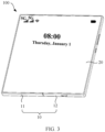
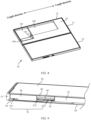
- FIG. 3 and FIG. 4 schematically show a structure of a foldable dual screen mobile phone in an unfolded state.
- an embodiment of this application provides an electronic device 100 with two screens, which may include, but is not limited to, a foldable fixed terminal or mobile terminal such as a mobile phone, a tablet computer, a notebook computer, an ultra-mobile personal computer (ultra-mobile personal computer, UMPC), a handheld computer, a touch TV, a walkie-talkie, a netbook, a POS terminal, a personal digital assistant (personal digital assistant, PDA), a wearable device, or a virtual reality device.
- a foldable fixed terminal or mobile terminal such as a mobile phone, a tablet computer, a notebook computer, an ultra-mobile personal computer (ultra-mobile personal computer, UMPC), a handheld computer, a touch TV, a walkie-talkie, a netbook, a POS terminal, a personal digital assistant (personal digital assistant, PDA), a wearable device, or a virtual
- the electronic device 100 includes a middle frame 10, a first display 20, and a second display 30.
- the middle frame 10 is configured to carry the first display 20 and the second display 30.
- the middle frame 10 includes a middle plate 14 (as shown in the following FIG. 8 ) and a frame 15 (as shown in the following FIG. 8 ), and the frame 15 is connected to an entire circumferential edge of the middle plate 14.
- the middle plate 14 may be a metal middle plate 14 made of a metal material such as aluminum or magnesium.
- the first display 20 and the second display 30 are respectively disposed on two sides of the metal middle plate 14, and are connected to the metal middle plate 14 in a manner such as bonding.
- Each of the first display 20 and the second display 30 may be an organic light-emitting diode (Organic Light-Emitting Diode, OLED) display or a liquid crystal display (Liquid Crystal Display, LCD).
- OLED Organic Light-Emitting Diode
- LCD Liquid Crystal Display
- one of the first display 20 and the second display 30 may be the OLED display or the LCD
- the other of the first display 20 and the second display 30 may be an E-Ink ink screen
- the OLED display or the LCD has high resolution
- the E-Ink ink screen has low reflectivity. Therefore, the user may use the OLED display or the LCD to view an image and read by using the E-Ink ink screen, to avoid damage to eyesight due to use of the OLED display or the LCD for reading for a long time.
- Sizes of the first display 20 and the second display 30 may be the same or may be different.
- a size of the second display 30 may be smaller than a size of the first display 20, and the first display 20 and the second display 30 can switch to display, to implement switching of the size of the screen. In this way, when the power of the electronic device 100 is relatively low, the user may use the second display 30 to reduce power consumption of the electronic device 100.
- the first display 20 and the second display 30 each may be a flexible display that can be folded, and the middle frame 10 may also be folded, so that the electronic device 100 can be folded.
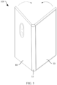
- FIG. 5 schematically shows a structure of a foldable mobile phone in a semi-folded state.
- the middle frame 10 includes a first structural member 11, a second structural member 12, and a rotating assembly 13 disposed between the first structural member 11 and the second structural member 12. Both the first structural member 11 and the second structural member 12 are rotatably connected to the rotating assembly 13, so that the first structural member 11 and the second structural member 12 can rotate relative to the rotating assembly 13.
- the first structural member 11 may be a first middle frame
- the second structural member 12 may be a second middle frame. Therefore, the first structural member 11 and the second structural member 12 each may include a middle plate 14 and a frame 15.
- FIG. 6 schematically shows a structure of a foldable mobile phone in a folded state.
- the first display 20 is a flexible display
- a size of the second display 30 is smaller than that of the first display 20
- the first structural member 11 and the second structural member 12 can rotate toward each other to be stacked on each other.
- the first display 20 can be bent and attached between the first structural member 11 and the second structural member 12, the second display 30 is exposed outside to display an image, and the mobile phone is in a folded state (for example, as shown in FIG. 5 ).
- the first structural member 11 and the second structural member 12 may further rotate away from each other from a stacked state to a state in which the first structural member 11 and the second structural member 12 are on a same plane.
- the first display 20 unfolds, and the mobile phone is in an unfolded state (for example, as shown in FIG. 3 ).
- the dual screen electronic device 100 provided in this embodiment may be an electronic device 100 that cannot be folded, or may be an electronic device 100 that can be folded.
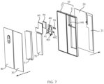
- FIG. 7 schematically shows a breakdown structure of an electronic device 100 according to an embodiment.
- the electronic device 100 further includes a mainboard 40.
- the mainboard 40 is mounted on the middle plate 14, and is disposed in parallel with the first display 20 and the second display 30.
- the mainboard 40 may be disposed on a side that is of the middle plate 14 and that faces the first display 20, or may be disposed on a side that is of the middle plate 14 and that faces the second display 30.
- the mainboard 40 may be a circuit board made of a flexible material, or may be a rigid printed circuit board (Printed Circuit Board; PCB).
- An electronic element 41 is disposed on the mainboard 40, and the electronic element 41 may be any one or more of a power amplifier, a central processing unit (Central Processing Unit; CPU), a power management integrated circuit (Power Management IC; PMIC), a universal flash storage (Universal Flash Storage; UFS), and an image signal processor (Image Signal Processor; ISP).
- a power amplifier Central Processing Unit; CPU
- CPU Central Processing Unit
- PMIC power management integrated circuit
- UFS Universal Flash Storage
- ISP Image Signal Processor
- the mainboard 40 is a double-sided board.
- the mainboard 40 has a first surface 401 and a second surface 402 that are disposed facing away from each other, and electronic elements 41 may be disposed on both the first surface 401 and the second surface 402.
- the first surface 401 refers to a surface that is of the mainboard 40 and that faces the first display 20.
- the second surface 402 refers to a surface that is of the mainboard 40 and that faces the second display 30.
- the mainboard 40 is electrically connected to both the first display 20 and the second display 30, to supply power to the first display 20 and the second display 30.
- a specific implementation is as follows: A first flexible printed circuit board 21 is disposed on a non-display surface of the first display 20, and the other end that is of the first flexible printed circuit board 21 and that is away from the first display 20 extends between the first display 20 and the mainboard 40, and is electrically connected to the first surface 401 of the mainboard 40; and a second flexible printed circuit board 31 is disposed on a non-display surface of the second display 30, and the other end that is of the second flexible printed circuit board 31 and that is away from the second display 30 extends between the second display 30 and the mainboard 40, and is electrically connected to the second surface 402 of the mainboard 40.
- the non-display surface of the first display 20 refers to a surface that is of the first display 20 and that faces the mainboard 40 and that is away from the outside
- the non-display surface of the second display 30 refers to a surface that is of the second display 30 and that faces the mainboard 40 and that faces the outside.
- the first flexible printed circuit board 21 and the second flexible printed circuit board 31 each is a printed circuit board made of a flexible insulation material, has relatively high flexibility, and can be freely bent, wound, and folded, so that the first flexible printed circuit board 21 can be bent and extend between the first display 20 and the mainboard 40, and the second flexible printed circuit board 31 can be bent and extend between the second display 30 and the mainboard 40.
- FIG. 8 schematically shows a three-dimensional structure of a middle frame 10. It should be noted that, as shown in FIG. 8 , an opening 140 is disposed on the middle plate 14, and a part of the mainboard 40 directly faces the opening 140, to ensure that the first flexible printed circuit board 21 and the second flexible printed circuit board 31 that are located on two sides of the middle plate 14 can be connected to the mainboard 40. Specifically, when the mainboard 40 is disposed on a side that is of the middle plate 14 and that faces the first display 20, the second flexible printed circuit board 31 can extend into the opening 140 to connect the second surface 402 of the mainboard 40. Similarly, referring to FIG. 9 and FIG.
- FIG. 9 schematically shows a schematic sectional view of an electronic device 100 taken along a direction L-L in FIG. 4 ; and FIG. 10 schematically shows a schematic sectional view of a breakdown structure of an electronic device 100 taken along a direction L-L in FIG. 4 .
- a shape of the opening 140 is not limited. The opening 140 may be in a regular shape such as a circular shape, a square, a rectangle, or a rounded rectangle, or may be in another irregular shape.
- both the first flexible printed circuit board 21 and the second flexible printed circuit board 31 of the electronic device 100 are connected to a surface that is opposite to the mainboard 40, and neither of the first flexible printed circuit board 21 and the second flexible printed circuit board 31 is wound around two sides of the mainboard 40.
- an example of the detachment process of the first display 20 may be as follows: A connection relationship between the first display 20 and the middle frame 10 is released, the first display 20 is moved in a positive direction (a direction shown by a solid arrow in FIG.
- the positive direction of the electronic device 100 refers to a direction that is of the first display 20 and that faces the user when the electronic device 100 is in an unfolded state.
- a reverse direction of the electronic device 100 refers to a direction that is of the second display 30 and that faces the user when the electronic device 100 is in an unfolded state.
- a process of reassembling the first display 20 on the middle frame 10 is as follows: The first display 20 is moved to a side of the middle frame 10, the first flexible printed circuit board 21 is connected to the first surface 401 of the mainboard 40, and then the first display 20 is connected to the middle frame 10.
- the second display 30 may be directly detached from the reverse direction of the electronic device 100.
- the second display 30 and the mainboard 40 may be sequentially detached and then the first display 20 is detached.
- the first display 20 can be directly detached from the positive direction of the electronic device 100.
- the first display 20 when the first display 20 is faulty and needs to be replaced or repaired, if the first display 20 is directly detached from a positive direction of the electronic device 100, components such as the second display 30 and the mainboard 40 do not need to be detached, and a detachment process is simple; in addition, this prevents electronic elements such as the mainboard 40 and the second display 30 from being damaged due to collision or scraping in the detachment process, thereby avoiding high repair costs.
- FIG. 11 schematically shows a three-dimensional structure of the first flexible printed circuit board 21.
- the first flexible printed circuit board 21 may include at least a bent segment 211 and a connection segment 212 that are connected. One end that is of the bent segment 211 and that is away from the connection segment 212 is connected to a non-display surface of the first display 20, the connection segment 212 extends between the first display 20 and the mainboard 40, and the connection segment 212 is connected to the first surface 401 of the mainboard 40.
- the bent segment 211 and a surface that is of the first display 20 and that faces the mainboard 40 may be connected in a bonding manner.
- a bent shape of the bent segment 211 is not limited.
- the bent segment 211 may have a bent angle (not shown in the figure), that is, the bent segment 211 is in a bent line shape, or in the example shown in FIG. 11 , the bent segment 211 may also be arc-shaped, and the bent segment 211 in the arc shape does not have a sharp angle, so as to avoid stress concentration at the bent angle of the bent segment 211. It may be understood that at least one bend may be formed on the bent segment 211. That is, in some embodiments, the bent segment 211 may have a plurality of bends, and bent shapes and bent angles of the plurality of bends may be the same or different.
- the bent segment 211 can be bent and extend, so that a redundant part is formed on the first flexible printed circuit board 21, and the redundant part can extend and be bent. Therefore, in a process of detaching the first display 20, when the first display 20 is moved in a positive direction of the electronic device 100 to move away from the mainboard 40, the bent segment 211 can extend with movement of the first display 20, so that a pulling force of the first display 20 on the first flexible printed circuit board 21 directly acts on a connection point between the connection segment 212 and the mainboard 40, thereby preventing the mainboard 40 from being pulled when the first display 20 is detached.
- a structure of the second flexible printed circuit board 31 may be the same as a structure of the first flexible printed circuit board 21. That is, for the structure of the second flexible printed circuit board 31, refer to the structure of the first flexible printed circuit board 21.
- the second flexible printed circuit board 31 may also include a mounting segment 311 and a bent segment 310 that are connected. One end that is of the bent segment 310 and that is away from the mounting segment 311 is connected to a non-display surface of the second display 30, and one end that is of the mounting segment 311 and that is away from the bent segment 310 is connected to a second surface 402 of the mainboard 40. Therefore, when the second display 30 is detached, a redundant part of the second flexible printed circuit board 31 can extend, to prevent the mainboard 40 from being pulled by the second flexible printed circuit board 31 when the second display 30 is detached.
- the first flexible printed circuit board 21 may further include a fastening segment 210, where the fastening segment 210 is fastened to a non-display surface of the first display 20, and the fastening segment 210 is connected to one end that is of the bent segment 211 and that is away from the connection segment 212.
- a connection portion between the first flexible printed circuit board 21 and the first display 20 is added, so that the first flexible printed circuit board 21 can be mounted more reliably.
- the fastening segment 210 may be configured to extend along any direction, provided that the fastening segment 210 can be connected to one end of the bent segment 211.
- the fastening segment 210 may extend along a length direction of the electronic device 100 to connect the mainboard 40, or the fastening segment 210 may extend along a width direction of the electronic device 100 to connect the mainboard 40.
- the fastening segment 210 and the connection segment 212 may be located on a same side of the bent segment 211, or the fastening segment 210 and the connection segment 212 may be respectively disposed on two sides of the bent segment 211.
- the electronic device 100 may further include a functional component 90.
- the functional component 90 is mounted on the middle plate 14, the functional component 90 and the mainboard 40 are disposed on a same side of the middle plate 14, and the functional component 90 and the mainboard 40 are disposed side by side along the length direction of the electronic device 100.
- the functional component 90 may be a speaker, and the electronic device 100 has a sound generation function.
- the functional component 90 may be a camera, and the electronic device 100 has a photographing function.
- the functional component 90 may be mounted on the middle plate 14 after the mainboard 40 is mounted on the middle plate 14; or the functional component 90 may be mounted on the middle plate 14 before the mainboard 40 is mounted on the middle plate 14.
- a thickness of the middle plate 14 may be the same everywhere, or thicknesses of at least two positions of the middle plate 14 may be different. In the example shown in FIG. 8 , thicknesses of all parts of the middle plate 14 are not completely the same, so that a first recess 141 is formed on the middle plate 14. Both the mainboard 40 and the functional component 90 are mounted in the first recess 141, and a projection of the first recess 141 on the middle plate 14 is slightly larger than projections of the mainboard 40 and the functional component 90 on the middle plate 14, so that a size of the first recess 141 can match sizes of the mainboard 40 and the functional component 90 that are disposed side by side. Therefore, mounting positions of the mainboard 40 and the functional component 90 can be identified accurately.
- a first recess 141 is formed on a surface that is of the middle plate 14 and that faces the first display 20, and the functional component 90 is correspondingly disposed on a side that is of the middle plate 14 and that faces the first display 20.
- the opening 140 may be aligned with only a part that is of the mainboard 40 and that is connected to the first flexible printed circuit board 21, to reduce a size of the opening 140 as much as possible, thereby ensuring that the middle frame 10 has relatively high strength to stably carry the mainboard 40 and the functional component 90.
- a first recess 141 is formed on a surface that is of the middle plate 14 and that faces the second display 30, and the functional component 90 is correspondingly disposed on a side that is of the middle plate 14 and that faces the second display 30.
- the opening 140 may alternatively be aligned with the functional component 90.
- a protruding portion 91 may protrude from a surface that is of the functional component 90 and that faces the first display 20, and the protruding portion 91 may extend from the opening 140 to a side that is of the middle plate 14 and that faces the first display 20, and the first display 20 can directly or indirectly support the protruding portion 91 to provide support for the functional component 90.
- the opening 140 is a rectangle or a rounded rectangle, and the opening 140 extends along a length direction of the electronic device 100, compared with the circular opening 140, the opening 140 can be as small as possible while being aligned with the functional component 90 and the mainboard 40, thereby ensuring that the middle frame 10 has a relatively high strength to stably carry the mainboard 40 and the functional component 90. It may be understood that, when the opening 140 is aligned with both the mainboard 40 and the functional component 90, the connection segment 212 of the first flexible printed circuit board 21 may completely face the opening 140.
- a positional relationship between the first flexible printed circuit board 21 and the first display 20 and the mainboard 40 may be as follows: In a first case, as shown in FIG. 12 , the entire first flexible printed circuit board 21 may be disposed between the first display 20 and the mainboard 40.
- FIG. 12 schematically shows another cross-sectional structure of an electronic device 100 along a direction L-L in FIG. 4 .
- the first flexible printed circuit board 21 includes only the connection segment 212 and the bent segment 211, both the connection segment 212 and the bent segment 211 are located between the first display 20 and the mainboard 40. If the first flexible printed circuit board 21 further includes a fastening segment 210, the connection segment 212, the bent segment 211, and the fastening segment 210 are all located between the first display 20 and the mainboard 40.
- the functional component 90 may be in direct contact with a non-display surface of the first display 20, and the functional component 90 and the first display 20 support each other.
- FIG. 13 schematically shows still another cross-sectional structure of an electronic device 100 along a direction L-L in FIG. 4 .
- parts of the bent segment 211 and the connection segment 212 are disposed between the functional component 90 and the first display 20, and the other part of the connection segment 212 is disposed between the first display 20 and the mainboard 40.
- the first flexible printed circuit board 21 is not limited between the mainboard 40 and the first display 20, and can extend in a larger space.
- the fastening segment 210 may extend between the functional component 90 and the first display 20.
- the fastening segment 210 and the connection segment 212 are located on a same side of the bent segment 211, a part of the fastening segment 210 may be located between the mainboard 40 and the first display 20, and the other part of the fastening segment 210 may be located between the functional component 90 and the first display 20.
- a part of the functional component 90 may be further configured to be jointly enclosed, with the first display 20, into an avoidance groove 92 for accommodating the bent segment 211, to prevent interference between the bent segment 211 and the functional component 90.
- the functional component 90 is provided with a protruding portion 91.
- a surface that is of the functional component 90 and that faces the first display 20 and the protruding portion 91 may jointly define a step surface.
- the step surface and the first display 20 are jointly enclosed into an avoidance groove 92, and the avoidance groove 92 is formed on the other side that is of the protruding portion 91 and that is away from the mainboard 40.
- connection segment 212 extends between the mainboard 40 and the first display 20, from the protruding portion 91 and the first display 20, and the protruding portion 91 of the functional component 90 abuts on a surface that is of the connection segment 212 and that is away from the first display 20.
- first flexible printed circuit board 21 further includes a fastening segment 210, and the fastening segment 210 and the connection segment 212 are located on a same side of the bent segment 211, the fastening segment 210 is connected to a non-display surface of the first display 20, and the connection segment 212 and the fastening segment 210 are sandwiched between the functional component 90 and the first display 20.
- the avoidance groove 92 may alternatively be disposed on a side that is of the functional component 90 and that is close to the mainboard 40, so that the avoidance groove 92 can be connected to a space between the mainboard 40 and the first display 20.
- the functional component 90 may be directly in contact with a non-display surface of the first display 20.
- FIG. 14 schematically shows a three-dimensional structure of a locking bracket 50.
- the electronic device 100 may further include a locking bracket 50, where the locking bracket 50 is disposed between the mainboard 40 and the first display 20, the locking bracket 50 is detachably connected to the middle frame 10, and is in contact with a surface that is of the connection segment 212 and that is away from the mainboard 40. In this way, the locking bracket 50 can press the connection segment 212, to prevent the first flexible printed circuit board 21 from loosening from the mainboard 40.
- FIG. 15 schematically shows breakdown structures of a locking bracket 50 and a middle frame 10. Referring to FIG. 10 and FIG. 15 , an example in which the opening 140 is a rectangle is used for description. The rectangular opening 140 extends along a length direction of the electronic device 100.
- the locking bracket 50 may extend along a width direction of the electronic device 100, and two ends of the locking bracket 50 extend to two sides of the opening 140, so that the locking bracket 50 crosses the opening 140, and a part of the locking bracket 50 can face the opening 140, and then the locking bracket 50 can face a part that is of the mainboard 40 and that is connected to the first flexible printed circuit board 21.
- one end that is of the connection segment 212 and that is away from the bent segment 211 may extend to the opening 140, and may be inserted between the mainboard 40 and the locking bracket 50.
- the first flexible printed circuit board 21 may be connected to the mainboard 40 by using the connector 42.
- the connector 42 may be, for example, a board-to-board connector 42 (board to board; BTB).
- the connector 42 includes a male socket 421 and a female socket 420 (as shown in the following FIG. 17a ).
- the male socket 421 is disposed on a non-display surface of the first flexible printed circuit board 21, the female socket 420 is disposed on a first surface 401 of the mainboard 40, and the female socket 420 may be inserted into the male socket 421, so that the first flexible printed circuit board 21 is electrically connected to the mainboard 40.
- a clamping gap may be defined between the locking bracket 50 and the mainboard 40, and the first flexible printed circuit board 21, the male socket 421, and the female socket 420 are clamped in the clamping gap.
- a joint between the first flexible printed circuit board 21 and the mainboard 40 may be clamped in the clamping gap, to prevent the male socket 421 of the connector 42 from being separated from the female socket 420, so that a connection between the first flexible printed circuit board 21 and the mainboard 40 is more reliable.
- the locking bracket 50 may be connected to a surface that is of the middle plate 14 and that faces the first display 20, so that the locking bracket 50 is located on a side that is of the middle plate 14 and that faces the first display 20.
- a first mounting base 143 and a second mounting base 143 protrude from a surface that is of the middle plate 14 and that faces the second display 30, and projections of the first mounting base 143 and the second mounting base 143 on the middle plate 14 are located in the opening 140.
- the locking bracket 50 may be accommodated in the opening 140, and two ends of the locking bracket 50 are detachably connected to the first mounting base 143 and the second mounting base 143, respectively.
- the first mounting base 143 may be a plate-like structure, or may be a block-like structure. This is not limited in this embodiment.
- the locking bracket 50 may be a flat plate-like structure.
- the locking bracket 50 may include a first plate body 51, a second plate body 52, and a middle plate body 53 located between the first plate body 51 and the second plate body 52. Two ends of the middle plate body 53 are respectively connected to the first plate body 51 and the second plate body 52, and a surface of the middle plate body 53 is different from surfaces of the first plate body 51 and the second plate body 52, so that a groove is formed on a surface that is of the locking bracket 50 and that faces the mainboard 40.
- a clamping gap can be enlarged as much as possible, so that the connector 42 and the connection segment 212 can be clamped in the clamping gap.
- the first mounting base 143 and the second mounting base 143 protrude from a surface that is of the middle plate 14 and that faces the first display 20, and two ends of the locking bracket 50 are connected to the first mounting base 143 and the second mounting base 143.
- each of the first mounting base 143 and the second mounting base 143, and the middle plate 14 may form an integrated component by using an integrated molding process. Therefore, steps of assembling the first mounting base 143 and the second mounting base 143 may be omitted, thereby improving assembly efficiency. In addition, strength of the middle plate 14 may be improved without increasing costs.
- a manner of detachable connection between the locking bracket 50 and the middle frame 10 is not limited to a screw connection, or may be a connection manner such as clamping.
- a screw hole 1430 is disposed on each of the first mounting base 143 and the second mounting base 143, and through holes 54 are disposed on two ends of the locking bracket 50.
- a screw hole 1430 of the first mounting base 143 is coaxial with a through hole 54 of one end of the locking bracket 50
- a screw hole 1430 of the second mounting base 143 is coaxial with a through hole 54 of the other end of the locking bracket 50.
- a screw may be connected to the screw hole 1430 after passing through the through hole 54, so that the locking bracket 50 is connected to the first mounting base 143 by using the screw.
- the second flexible printed circuit board 31 may be electrically connected to the second surface 402 of the mainboard 40 by using the connector 42.
- a female socket 420 is disposed on the second surface 402 of the mainboard 40, and a male socket 421 that can be inserted into the female socket 420 is disposed on a surface that is of the second flexible printed circuit board 31 and that faces the mainboard 40, so that the second flexible printed circuit board 31 is electrically connected to the mainboard 40.
- the electronic device 100 may further include a cover plate 60, where the cover plate 60 is disposed between the mainboard 40 and the second display 30, and the cover plate 60 presses the second surface 402 of the mainboard 40.
- the cover plate 60 can prevent the mainboard 40 from abutting on the second display 30, to ensure that the second display 30 and the middle frame 10 are reliably connected.
- the cover 60 can press a joint between the second display 30 and the mainboard 40, to prevent loosening of the connector 42 between the second display 30 and the mainboard 40, so that a connection between the second flexible printed circuit board 31 and the mainboard 40 is more reliable.
- the mounting segment 311 of the second flexible printed circuit board 31 can extend from a gap between the frame 10 and the cover plate 60 into the mainboard 40 and the cover plate 60, to connect the mainboard 40.
- the second flexible printed circuit board 31 surrounds an edge of a side of the cover plate 60.
- a via hole (not shown in the figure) may further be disposed on the cover plate 60, and a mounting segment 311 of the second flexible printed circuit board 31 may extend between the mainboard 40 and the cover plate 60 through the via hole.
- the electronic device 100 may further include a rear cover 80, and the rear cover 80 is disposed on a side that is of the middle plate 14 and that faces the second display 30.
- the rear cover 80 may be mounted on the other side of the middle frame 10, and the second display 30 may be mounted on the rear cover 80.
- a size of the second display 30 may be smaller than a size of the first display 20.
- the middle frame 10 may include, for example, a first structural member 11 and a second structural member 12, and the second display 30 and the rear cover 80 may be mounted on the first structural member 11 and the second structural member 12, respectively.
- the first structural member 11 and the second structural member 12 can rotate to a same plane, and correspondingly, the rear cover 80 and the second display 30 are also located on a same plane.
- the electronic device 100 may further include a battery 70.
- the battery 70 and the mainboard 40 are disposed on a same side of the middle plate 14, and the battery 70 is electrically connected to the mainboard 40 to supply power to the mainboard 40.
- thicknesses of all parts of the middle plate 14 are not completely the same, so that a first recess 141 is formed on the middle plate 14, and a second recess 142 is also formed on the middle plate 14, where the battery 70 is mounted in the second recess 142.
- the middle frame 10 includes the first structural member 11 and the second structural member 12, the second recess 142 may be formed on the first structural member 11.
- the battery 70 is also disposed between the second display 30 and the first display 20.
- the second recess 142 may be formed on the second structural member 12.
- the battery 70 is disposed between the first display 20 and the rear cover 80.
- the rear cover 80 may also be referred to as a cover of the battery 70.
- FIG. 16a to FIG. 16d schematically show a detachment process of a first display 20 of an electronic device 100.
- the first display 20 needs to be repaired or replaced due to crack, scraping, poor contact, or another reason
- another example of the detachment process of the first display 20 may be as follows: As shown in FIG. 16a , the electronic device 100 is first provided, and the first display 20 faces a direction in which the user is located, to facilitate subsequent detachment.
- the first flexible printed circuit board 21 has a redundant part, and the redundant part can extend with movement of the first display 20, to alleviate a pulling force on the first flexible printed circuit board 21, thereby preventing the mainboard 40 from being pulled.
- a force is exerted on the connection segment 212 of the first flexible printed circuit board 21, so that the male socket 421 of the connector 42 is released from the female socket 420, and then the first flexible printed circuit board 21 is disengaged from the mainboard 40, so that the first display 20 is detached.
- an assembly sequence of a reassembly process of the first display 20 may be reverse to a detachment process of the first display 20.
- an example of the reassembly process of the first display 20 is as follows: First, the male socket 421 on the first flexible printed circuit board 21 is buckled with the female socket 420 on the mainboard 40, and the male socket 421 and the female socket 420 jointly form the connector 42, so that the first flexible printed circuit board 21 is connected to the mainboard 40; then the locking bracket 50 is detachably connected to the middle frame 10, so that a joint between the first flexible printed circuit board 21 and the mainboard 40 is pressed by the locking bracket 50; then the first display 20 is moved to make the first display 20 opposite to the middle plate 14; and then the first display 20 is connected to the middle plate 10, to complete reassembly of the first display 20.
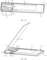
- FIG. 17a to FIG. 17e schematically show an assembly process of an electronic device 100.
- An example of the assembly process of the electronic device 100 provided in this embodiment is as follows: As shown in FIG.
- the locking bracket 50 is connected to the middle frame 10, and then the first display 20 is moved to a side of the middle frame 10, so that the first display 20 is opposite to the middle plate 14, and one end that is of the connection segment 212 and that is away from the bent segment 211 is attached to the locking bracket 50; and the mainboard 40 is moved to a side that is of the first display 20 and that faces the middle frame 10, so that a preset included angle ⁇ exists between the first surface 401 of the mainboard 40 and a surface that is of the middle plate 14 and that is away from the first display 20; and then, as shown in FIG. 17b and FIG. 17c , the mainboard 40 is rotated until the mainboard 40 is in contact with the middle plate 14.
- a preset angle may be greater than or equal to 45 degrees and less than or equal to 120 degrees. When the preset angle is 90 degrees, the mainboard 40 is first erected vertically during mounting.
- the functional component 90 is mounted in the first recess 141, and the battery 70 is mounted in the second recess 142; and then the second display 30 is moved to the other side of the middle frame 10, so that the mounting segment 311 of the second flexible printed circuit board 31 is connected to the second surface 402 of the mainboard 40.
- the second flexible printed circuit board 31 also has a redundant part, the second flexible printed circuit board 31 can extend to enable the second display 30 to be inclined to the middle plate 14, and a space can be provided between the second display 30 and the middle plate 14, so that another part can perform a mounting operation in the space.
- the cover plate 60 is mounted on a side that is of the mainboard 40 and that is away from the first display 20, so that the cover plate 60 covers on the mainboard 40; then the second display 30 is moved to make the second display 30 face the middle plate 14; and then the second display 30 is connected to the middle plate 10, to complete mounting of the electronic device 100.
- the terms “mount”, “connected to” and “connect” should be understood in a broad sense, and for example, may be a fixed connection or an indirect connection by using an intermediate medium, or may be internal communication between two elements or an interaction relationship between two elements.
- the terms “mount”, “connected to” and “connect” should be understood in a broad sense, and for example, may be a fixed connection or an indirect connection by using an intermediate medium, or may be internal communication between two elements or an interaction relationship between two elements.
- a process, a method, a system, a product, or a device that includes a series of steps or units is not necessarily limited to those steps or units that are clearly listed, but may include other steps or units that are not clearly listed or are inherent to the process, method, product, or device.
- a plurality of in this specification refers to two or more.
- the term “and/or” in this specification describes only an association relationship for describing associated objects and represents that three relationships can exist. For example, “A and/or B” can represent the following three cases: Only A exists, both A and B exist, and only B exists.
- the character “/” in this specification usually indicates an "or” relationship between the associated objects. In a formula, the character "/" indicates that the associated objects are in a "division" relationship.
Landscapes
- Engineering & Computer Science (AREA)
- Signal Processing (AREA)
- Devices For Indicating Variable Information By Combining Individual Elements (AREA)
Claims (15)
- Un dispositif électronique (100), comprenant :un cadre intermédiaire (10), comprenant une plaque intermédiaire (14) et un cadre (15) connecté à un bord circonférentiel de la plaque intermédiaire (14), une ouverture (140) étant disposée sur la plaque intermédiaire (14) ;un premier écran (20) et un second écran (30), respectivement disposés sur deux côtés de la plaque intermédiaire (14) ;une carte mère (40), montée sur la plaque intermédiaire (14) et faisant face à l'ouverture (140) ;un premier circuit imprimé flexible (21), dont une extrémité est connectée à une surface du premier écran (20) faisant face à la plaque intermédiaire (14), et l'autre extrémité du premier circuit imprimé flexible (21) s'étend entre le premier écran (20) et la carte mère (40) et est électriquement connectée à une surface de la carte mère (40) faisant face au premier écran (20) ; etun second circuit imprimé flexible (31), dont une extrémité est connectée à une surface du second écran (30) faisant face à la plaque intermédiaire (14), et l'autre extrémité du second circuit imprimé flexible (31) s'étend entre le second écran (30) et la carte mère (40) et est électriquement connectée à une surface de la carte mère (40) faisant face au second écran (30).
- Le dispositif électronique (100) selon la revendication 1, comprenant en outre un support de verrouillage (50) disposé entre la carte mère (40) et le premier écran (20), le support de verrouillage (50) étant connecté de manière détachable au cadre intermédiaire (10), et le support de verrouillage (50) étant en contact avec une surface du premier circuit imprimé flexible (21) faisant face au premier écran (20).
- Le dispositif électronique (100) selon la revendication 2, dans lequel une première base de montage (143) et une seconde base de montage (143) dépassent de la plaque intermédiaire (14), la première base de montage (143) et la seconde base de montage (143) étant disposées sur deux côtés opposés à l'ouverture (140), et les deux extrémités du support de verrouillage (50) étant connectées de manière détachable à la première base de montage (143) et à la seconde base de montage (143), respectivement.
- Le dispositif électronique (100) selon la revendication 3, dans lequel chacune des première base de montage (143) et seconde base de montage (143), et la plaque intermédiaire (14) forment un composant intégré en utilisant un processus de moulage intégré.
- Le dispositif électronique (100) selon l'une quelconque des revendications 2 à 4, dans lequel le premier circuit imprimé flexible (21) est connecté à la surface de la carte mère (40) faisant face au premier écran (20) à l'aide d'un connecteur (42), le connecteur (42) comprenant une prise mâle (421) et une prise femelle (420), la prise mâle (421) étant disposée sur une surface du premier circuit imprimé flexible (21) faisant face à la carte mère (40), la prise femelle (420) étant disposée sur la surface de la carte mère (40) faisant face au premier écran (20), et la prise femelle (420) étant insérée dans la prise mâle (421) ; et
un espace de serrage est défini conjointement entre le support de verrouillage (50) et la carte mère (40), et le premier circuit imprimé flexible (21) ainsi que le connecteur (42) sont serrés dans cet espace de serrage. - Le dispositif électronique (100) selon l'une quelconque des revendications 1 à 5, comprenant en outre une plaque de recouvrement (60) disposée entre la carte mère (40) et le second écran (30), la plaque de recouvrement (60) recouvrant la carte mère (40).
- Le dispositif électronique (100) selon l'une quelconque des revendications 1 à 6, dans lequel le premier circuit imprimé flexible (21) comprend un segment plié (211) et un segment de connexion (212) qui sont connectés, une extrémité du segment plié (211) éloignée du segment de connexion (212) étant connectée au premier écran (20), et le segment de connexion (212) étant électriquement connecté à la surface de la carte mère (40) faisant face au premier écran (20).
- Le dispositif électronique (100) selon la revendication 7, dans lequel le segment plié (211) et le segment de connexion (212) sont tous deux situés entre la carte mère (40) et le premier écran (20).
- Le dispositif électronique (100) selon la revendication 7, comprenant en outre un composant fonctionnel (90), dans lequel le composant fonctionnel (90) et la carte mère (40) sont situés du même côté de la plaque intermédiaire (14), le composant fonctionnel (90) et la carte mère (40) étant disposés côte à côte le long d'une direction longitudinale du dispositif électronique (100), et le segment plié (211) ainsi qu'une partie du segment de connexion (212) étant disposés entre le composant fonctionnel (90) et le premier écran (20).
- Le dispositif électronique (100) selon la revendication 9, dans lequel la carte mère (40) et le deuxième écran (30) sont situés du même côté de la plaque intermédiaire (14), le composant fonctionnel (90) fait face à l'ouverture (140), une partie saillante (91) est disposée sur une surface du composant fonctionnel (90) qui fait face au premier écran (20), la partie saillante (91) s'étend de l'ouverture (140) vers un côté de la plaque intermédiaire (14) qui fait face au premier écran (20), une surface du composant fonctionnel (90) qui fait face au premier écran (20) et la partie saillante (91) définissent conjointement une surface en escalier, la surface en escalier et le premier écran (20) sont conjointement enfermés dans une rainure d'évitement (92), et le segment courbé (211) est disposé dans la rainure d'évitement (92).
- Le dispositif électronique (100) selon la revendication 10, dans lequel le segment courbé (211) est situé sur un côté de la partie saillante (91) qui est éloigné de la carte mère (40), le segment de connexion (212) s'étend d'une position entre la partie saillante (91) et le premier écran (20) à une position entre la carte mère (40) et le premier écran (20), et une surface du segment de connexion (212) qui fait face à la carte mère (40) est attachée à la partie saillante (91).
- Le dispositif électronique (100) selon l'une quelconque des revendications 7 à 11, dans lequel le premier circuit imprimé flexible (21) comprend un segment de fixation (210), le segment de fixation (210) est connecté à une surface du premier écran (20) qui fait face à la carte mère (40), et le segment de fixation (210) est connecté à une extrémité du segment courbé (211) qui est éloignée du segment de connexion (212).
- Le dispositif électronique (100) selon l'une quelconque des revendications 9 à 12, dans lequel le composant fonctionnel (90) est une caméra, ou le composant fonctionnel (90) est un haut-parleur.
- Le dispositif électronique (100) selon l'une quelconque des revendications 1 à 13, comprenant en outre une batterie (70) et un couvercle arrière (80), dans lequel la batterie (70) et la carte mère (40) sont disposées du même côté de la plaque intermédiaire (14), et la batterie (70) est connectée électriquement à la carte mère (40);
le couvercle arrière (80) et le deuxième écran (30) sont situés du même côté de la plaque intermédiaire (14); et la batterie (70) est disposée entre le couvercle arrière et le premier écran (20), ou la batterie (70) est disposée entre le premier écran (20) et le deuxième écran (30). - Le dispositif électronique (100) selon la revendication 14, dans lequel le premier écran (20) est un écran flexible pouvant être plié, le cadre central (10) comprend un premier élément structurel (11), un ensemble rotatif (13) et un second élément structurel (12), et le premier élément structurel (11) est relié de manière rotative au second élément structurel (12) à l'aide de l'ensemble rotatif (13).
Applications Claiming Priority (2)
| Application Number | Priority Date | Filing Date | Title |
|---|---|---|---|
| CN202111152373.7A CN115022427B (zh) | 2021-09-29 | 2021-09-29 | 电子设备 |
| PCT/CN2022/118095 WO2023051218A1 (fr) | 2021-09-29 | 2022-09-09 | Dispositif électronique |
Publications (3)
| Publication Number | Publication Date |
|---|---|
| EP4236277A1 EP4236277A1 (fr) | 2023-08-30 |
| EP4236277A4 EP4236277A4 (fr) | 2024-06-05 |
| EP4236277B1 true EP4236277B1 (fr) | 2025-04-30 |
Family
ID=83064483
Family Applications (1)
| Application Number | Title | Priority Date | Filing Date |
|---|---|---|---|
| EP22874605.3A Active EP4236277B1 (fr) | 2021-09-29 | 2022-09-09 | Dispositif électronique |
Country Status (4)
| Country | Link |
|---|---|
| US (1) | US20240007550A1 (fr) |
| EP (1) | EP4236277B1 (fr) |
| CN (1) | CN115022427B (fr) |
| WO (1) | WO2023051218A1 (fr) |
Families Citing this family (4)
| Publication number | Priority date | Publication date | Assignee | Title |
|---|---|---|---|---|
| CN115022427B (zh) * | 2021-09-29 | 2023-05-23 | 荣耀终端有限公司 | 电子设备 |
| CN115579228A (zh) * | 2021-10-28 | 2023-01-06 | 荣耀终端有限公司 | 电子设备 |
| CN115966139B (zh) * | 2022-12-16 | 2026-02-27 | 维沃移动通信有限公司 | 折叠屏电子设备 |
| WO2025187523A1 (fr) * | 2024-03-06 | 2025-09-12 | ソニーグループ株式会社 | Dispositif électronique |
Family Cites Families (16)
| Publication number | Priority date | Publication date | Assignee | Title |
|---|---|---|---|---|
| CA2778860A1 (fr) * | 2012-05-29 | 2013-11-29 | Ronald Sik Hung Yuen | Ecran d'affichage flexible |
| KR102415651B1 (ko) * | 2015-07-01 | 2022-07-01 | 엘지전자 주식회사 | 이동 단말기 |
| US9872408B2 (en) * | 2015-10-02 | 2018-01-16 | Samsung Electronics Co., Ltd. | Electronic device including waterproof structure |
| CN205812104U (zh) * | 2016-06-02 | 2016-12-14 | 上海与德通讯技术有限公司 | 一种移动终端 |
| CN206282195U (zh) * | 2016-12-27 | 2017-06-27 | 张振海 | 电子显示结构及手持电子设备 |
| CN106973170B (zh) * | 2017-06-02 | 2020-06-30 | 青岛海信移动通信技术股份有限公司 | 移动终端及其听筒控制方法 |
| CN110417943B (zh) * | 2018-04-27 | 2021-10-15 | Oppo广东移动通信有限公司 | 一种电子设备 |
| CN209593489U (zh) * | 2018-10-26 | 2019-11-05 | Oppo广东移动通信有限公司 | 折叠装置及电子设备 |
| CN211429360U (zh) * | 2020-03-09 | 2020-09-04 | Oppo广东移动通信有限公司 | 电子设备 |
| CN213150201U (zh) * | 2020-10-30 | 2021-05-07 | 京东方科技集团股份有限公司 | 显示装置 |
| CN112433402B (zh) * | 2020-11-10 | 2022-11-22 | 京东方科技集团股份有限公司 | 柔性电路板、显示组件及多屏显示设备 |
| CN112421321B (zh) * | 2020-11-30 | 2022-09-30 | 维沃移动通信有限公司 | 卡座装置和电子设备 |
| CN213783702U (zh) * | 2020-12-22 | 2021-07-23 | Oppo广东移动通信有限公司 | 电路板组件及电子设备 |
| CN113055511B (zh) * | 2021-03-11 | 2023-06-16 | 维沃移动通信有限公司 | 电路板组件和电子设备 |
| CN117796165A (zh) * | 2021-08-10 | 2024-03-29 | 三星电子株式会社 | 具有防水结构的电子装置 |
| CN115022427B (zh) * | 2021-09-29 | 2023-05-23 | 荣耀终端有限公司 | 电子设备 |
-
2021
- 2021-09-29 CN CN202111152373.7A patent/CN115022427B/zh active Active
-
2022
- 2022-09-09 US US18/253,409 patent/US20240007550A1/en active Pending
- 2022-09-09 WO PCT/CN2022/118095 patent/WO2023051218A1/fr not_active Ceased
- 2022-09-09 EP EP22874605.3A patent/EP4236277B1/fr active Active
Also Published As
| Publication number | Publication date |
|---|---|
| WO2023051218A9 (fr) | 2023-06-22 |
| CN115022427B (zh) | 2023-05-23 |
| CN115022427A (zh) | 2022-09-06 |
| US20240007550A1 (en) | 2024-01-04 |
| WO2023051218A1 (fr) | 2023-04-06 |
| EP4236277A1 (fr) | 2023-08-30 |
| EP4236277A4 (fr) | 2024-06-05 |
Similar Documents
| Publication | Publication Date | Title |
|---|---|---|
| EP4236277A1 (fr) | Dispositif électronique | |
| US11355888B2 (en) | Connector assembly, power supply assembly and electronic device | |
| US8564941B2 (en) | Electronic apparatus | |
| WO2022068497A1 (fr) | Dispositif électronique | |
| US9192061B2 (en) | Electronic device | |
| CN212034155U (zh) | 折叠机构、壳体、电子装置 | |
| US11281265B2 (en) | Electronic device with reduced chassis thickness | |
| JPH03151695A (ja) | プレーナ・ボードの支持装置 | |
| EP3582062A1 (fr) | Terminal | |
| CN101663632B (zh) | 电子设备 | |
| EP4117258B1 (fr) | Appareil électronique | |
| US7952654B2 (en) | Information processing apparatus and manufacturing method thereof | |
| EP3285117B1 (fr) | Ensemble carte à circuit imprimé et terminal | |
| WO2025161743A1 (fr) | Dispositif électronique pliable | |
| CN212034150U (zh) | 折叠机构、壳体、电子装置 | |
| CN108563356A (zh) | 显示屏组件及电子设备 | |
| HK40078687A (en) | Electronic device | |
| HK40078687B (en) | Electronic device | |
| JP3758043B2 (ja) | 電子機器およびその組立方法 | |
| US10841469B2 (en) | Image module and electronic device | |
| CN212034154U (zh) | 折叠机构、壳体、电子装置 | |
| US20220163998A1 (en) | Body panels with connectors | |
| CN223797667U (zh) | 电路板组件及终端设备 | |
| US7417874B2 (en) | Information processing apparatus having detachable front and rear covers | |
| CN212034152U (zh) | 电子装置 |
Legal Events
| Date | Code | Title | Description |
|---|---|---|---|
| STAA | Information on the status of an ep patent application or granted ep patent |
Free format text: STATUS: THE INTERNATIONAL PUBLICATION HAS BEEN MADE |
|
| PUAI | Public reference made under article 153(3) epc to a published international application that has entered the european phase |
Free format text: ORIGINAL CODE: 0009012 |
|
| STAA | Information on the status of an ep patent application or granted ep patent |
Free format text: STATUS: REQUEST FOR EXAMINATION WAS MADE |
|
| 17P | Request for examination filed |
Effective date: 20230522 |
|
| AK | Designated contracting states |
Kind code of ref document: A1 Designated state(s): AL AT BE BG CH CY CZ DE DK EE ES FI FR GB GR HR HU IE IS IT LI LT LU LV MC MK MT NL NO PL PT RO RS SE SI SK SM TR |
|
| A4 | Supplementary search report drawn up and despatched |
Effective date: 20240507 |
|
| RIC1 | Information provided on ipc code assigned before grant |
Ipc: H05K 1/11 20060101ALI20240430BHEP Ipc: H04M 1/03 20060101ALI20240430BHEP Ipc: H04M 1/02 20060101AFI20240430BHEP |
|
| GRAP | Despatch of communication of intention to grant a patent |
Free format text: ORIGINAL CODE: EPIDOSNIGR1 |
|
| STAA | Information on the status of an ep patent application or granted ep patent |
Free format text: STATUS: GRANT OF PATENT IS INTENDED |
|
| DAV | Request for validation of the european patent (deleted) | ||
| DAX | Request for extension of the european patent (deleted) | ||
| INTG | Intention to grant announced |
Effective date: 20241121 |
|
| GRAS | Grant fee paid |
Free format text: ORIGINAL CODE: EPIDOSNIGR3 |
|
| GRAA | (expected) grant |
Free format text: ORIGINAL CODE: 0009210 |
|
| STAA | Information on the status of an ep patent application or granted ep patent |
Free format text: STATUS: THE PATENT HAS BEEN GRANTED |
|
| AK | Designated contracting states |
Kind code of ref document: B1 Designated state(s): AL AT BE BG CH CY CZ DE DK EE ES FI FR GB GR HR HU IE IS IT LI LT LU LV MC MK MT NL NO PL PT RO RS SE SI SK SM TR |
|
| REG | Reference to a national code |
Ref country code: CH Ref legal event code: EP Ref country code: GB Ref legal event code: FG4D |
|
| REG | Reference to a national code |
Ref country code: IE Ref legal event code: FG4D |
|
| REG | Reference to a national code |
Ref country code: DE Ref legal event code: R096 Ref document number: 602022014039 Country of ref document: DE |
|
| REG | Reference to a national code |
Ref country code: NL Ref legal event code: FP |
|
| PGFP | Annual fee paid to national office [announced via postgrant information from national office to epo] |
Ref country code: NL Payment date: 20250814 Year of fee payment: 4 |
|
| REG | Reference to a national code |
Ref country code: AT Ref legal event code: MK05 Ref document number: 1791156 Country of ref document: AT Kind code of ref document: T Effective date: 20250430 |
|
| PG25 | Lapsed in a contracting state [announced via postgrant information from national office to epo] |
Ref country code: FI Free format text: LAPSE BECAUSE OF FAILURE TO SUBMIT A TRANSLATION OF THE DESCRIPTION OR TO PAY THE FEE WITHIN THE PRESCRIBED TIME-LIMIT Effective date: 20250430 Ref country code: ES Free format text: LAPSE BECAUSE OF FAILURE TO SUBMIT A TRANSLATION OF THE DESCRIPTION OR TO PAY THE FEE WITHIN THE PRESCRIBED TIME-LIMIT Effective date: 20250430 Ref country code: PT Free format text: LAPSE BECAUSE OF FAILURE TO SUBMIT A TRANSLATION OF THE DESCRIPTION OR TO PAY THE FEE WITHIN THE PRESCRIBED TIME-LIMIT Effective date: 20250901 |
|
| PGFP | Annual fee paid to national office [announced via postgrant information from national office to epo] |
Ref country code: DE Payment date: 20250730 Year of fee payment: 4 |
|
| REG | Reference to a national code |
Ref country code: LT Ref legal event code: MG9D |
|
| PG25 | Lapsed in a contracting state [announced via postgrant information from national office to epo] |
Ref country code: NO Free format text: LAPSE BECAUSE OF FAILURE TO SUBMIT A TRANSLATION OF THE DESCRIPTION OR TO PAY THE FEE WITHIN THE PRESCRIBED TIME-LIMIT Effective date: 20250730 Ref country code: GR Free format text: LAPSE BECAUSE OF FAILURE TO SUBMIT A TRANSLATION OF THE DESCRIPTION OR TO PAY THE FEE WITHIN THE PRESCRIBED TIME-LIMIT Effective date: 20250731 |
|
| PG25 | Lapsed in a contracting state [announced via postgrant information from national office to epo] |
Ref country code: PL Free format text: LAPSE BECAUSE OF FAILURE TO SUBMIT A TRANSLATION OF THE DESCRIPTION OR TO PAY THE FEE WITHIN THE PRESCRIBED TIME-LIMIT Effective date: 20250430 |
|
| PG25 | Lapsed in a contracting state [announced via postgrant information from national office to epo] |
Ref country code: BG Free format text: LAPSE BECAUSE OF FAILURE TO SUBMIT A TRANSLATION OF THE DESCRIPTION OR TO PAY THE FEE WITHIN THE PRESCRIBED TIME-LIMIT Effective date: 20250430 |
|
| PG25 | Lapsed in a contracting state [announced via postgrant information from national office to epo] |
Ref country code: HR Free format text: LAPSE BECAUSE OF FAILURE TO SUBMIT A TRANSLATION OF THE DESCRIPTION OR TO PAY THE FEE WITHIN THE PRESCRIBED TIME-LIMIT Effective date: 20250430 |
|
| PG25 | Lapsed in a contracting state [announced via postgrant information from national office to epo] |
Ref country code: AT Free format text: LAPSE BECAUSE OF FAILURE TO SUBMIT A TRANSLATION OF THE DESCRIPTION OR TO PAY THE FEE WITHIN THE PRESCRIBED TIME-LIMIT Effective date: 20250430 |
|
| PG25 | Lapsed in a contracting state [announced via postgrant information from national office to epo] |
Ref country code: RS Free format text: LAPSE BECAUSE OF FAILURE TO SUBMIT A TRANSLATION OF THE DESCRIPTION OR TO PAY THE FEE WITHIN THE PRESCRIBED TIME-LIMIT Effective date: 20250731 |
|
| PG25 | Lapsed in a contracting state [announced via postgrant information from national office to epo] |
Ref country code: IS Free format text: LAPSE BECAUSE OF FAILURE TO SUBMIT A TRANSLATION OF THE DESCRIPTION OR TO PAY THE FEE WITHIN THE PRESCRIBED TIME-LIMIT Effective date: 20250830 |
|
| PG25 | Lapsed in a contracting state [announced via postgrant information from national office to epo] |
Ref country code: LV Free format text: LAPSE BECAUSE OF FAILURE TO SUBMIT A TRANSLATION OF THE DESCRIPTION OR TO PAY THE FEE WITHIN THE PRESCRIBED TIME-LIMIT Effective date: 20250430 |
|
| PG25 | Lapsed in a contracting state [announced via postgrant information from national office to epo] |
Ref country code: DK Free format text: LAPSE BECAUSE OF FAILURE TO SUBMIT A TRANSLATION OF THE DESCRIPTION OR TO PAY THE FEE WITHIN THE PRESCRIBED TIME-LIMIT Effective date: 20250430 Ref country code: SM Free format text: LAPSE BECAUSE OF FAILURE TO SUBMIT A TRANSLATION OF THE DESCRIPTION OR TO PAY THE FEE WITHIN THE PRESCRIBED TIME-LIMIT Effective date: 20250430 |
|
| PG25 | Lapsed in a contracting state [announced via postgrant information from national office to epo] |
Ref country code: CZ Free format text: LAPSE BECAUSE OF FAILURE TO SUBMIT A TRANSLATION OF THE DESCRIPTION OR TO PAY THE FEE WITHIN THE PRESCRIBED TIME-LIMIT Effective date: 20250430 |
|
| PG25 | Lapsed in a contracting state [announced via postgrant information from national office to epo] |
Ref country code: EE Free format text: LAPSE BECAUSE OF FAILURE TO SUBMIT A TRANSLATION OF THE DESCRIPTION OR TO PAY THE FEE WITHIN THE PRESCRIBED TIME-LIMIT Effective date: 20250430 |
|
| PG25 | Lapsed in a contracting state [announced via postgrant information from national office to epo] |
Ref country code: SK Free format text: LAPSE BECAUSE OF FAILURE TO SUBMIT A TRANSLATION OF THE DESCRIPTION OR TO PAY THE FEE WITHIN THE PRESCRIBED TIME-LIMIT Effective date: 20250430 |
|
| PG25 | Lapsed in a contracting state [announced via postgrant information from national office to epo] |
Ref country code: IT Free format text: LAPSE BECAUSE OF FAILURE TO SUBMIT A TRANSLATION OF THE DESCRIPTION OR TO PAY THE FEE WITHIN THE PRESCRIBED TIME-LIMIT Effective date: 20250430 |
|
| REG | Reference to a national code |
Ref country code: DE Ref legal event code: R097 Ref document number: 602022014039 Country of ref document: DE |
|
| PG25 | Lapsed in a contracting state [announced via postgrant information from national office to epo] |
Ref country code: RO Free format text: LAPSE BECAUSE OF FAILURE TO SUBMIT A TRANSLATION OF THE DESCRIPTION OR TO PAY THE FEE WITHIN THE PRESCRIBED TIME-LIMIT Effective date: 20250430 |
|
| PLBE | No opposition filed within time limit |
Free format text: ORIGINAL CODE: 0009261 |
|
| STAA | Information on the status of an ep patent application or granted ep patent |
Free format text: STATUS: NO OPPOSITION FILED WITHIN TIME LIMIT |
|
| REG | Reference to a national code |
Ref country code: CH Ref legal event code: L10 Free format text: ST27 STATUS EVENT CODE: U-0-0-L10-L00 (AS PROVIDED BY THE NATIONAL OFFICE) Effective date: 20260311 |
|
| 26N | No opposition filed |
Effective date: 20260202 |
|
| REG | Reference to a national code |
Ref country code: CH Ref legal event code: H13 Free format text: ST27 STATUS EVENT CODE: U-0-0-H10-H13 (AS PROVIDED BY THE NATIONAL OFFICE) Effective date: 20260504 |