EP4239111A1 - Verfahren zur bewertung von siliciumcarbidsubstraten - Google Patents
Verfahren zur bewertung von siliciumcarbidsubstraten Download PDFInfo
- Publication number
- EP4239111A1 EP4239111A1 EP21886282.9A EP21886282A EP4239111A1 EP 4239111 A1 EP4239111 A1 EP 4239111A1 EP 21886282 A EP21886282 A EP 21886282A EP 4239111 A1 EP4239111 A1 EP 4239111A1
- Authority
- EP
- European Patent Office
- Prior art keywords
- sic substrate
- silicon carbide
- evaluating
- image
- carbide substrate
- Prior art date
- Legal status (The legal status is an assumption and is not a legal conclusion. Google has not performed a legal analysis and makes no representation as to the accuracy of the status listed.)
- Pending
Links
Images





Classifications
-
- H—ELECTRICITY
- H10—SEMICONDUCTOR DEVICES; ELECTRIC SOLID-STATE DEVICES NOT OTHERWISE PROVIDED FOR
- H10P—GENERIC PROCESSES OR APPARATUS FOR THE MANUFACTURE OR TREATMENT OF DEVICES COVERED BY CLASS H10
- H10P74/00—Testing or measuring during manufacture or treatment of wafers, substrates or devices
- H10P74/20—Testing or measuring during manufacture or treatment of wafers, substrates or devices characterised by the properties tested or measured, e.g. structural or electrical properties
- H10P74/203—Structural properties, e.g. testing or measuring thicknesses, line widths, warpage, bond strengths or physical defects
-
- G—PHYSICS
- G01—MEASURING; TESTING
- G01N—INVESTIGATING OR ANALYSING MATERIALS BY DETERMINING THEIR CHEMICAL OR PHYSICAL PROPERTIES
- G01N23/00—Investigating or analysing materials by the use of wave or particle radiation, e.g. X-rays or neutrons, not covered by groups G01N3/00 – G01N17/00, G01N21/00 or G01N22/00
- G01N23/22—Investigating or analysing materials by the use of wave or particle radiation, e.g. X-rays or neutrons, not covered by groups G01N3/00 – G01N17/00, G01N21/00 or G01N22/00 by measuring secondary emission from the material
- G01N23/225—Investigating or analysing materials by the use of wave or particle radiation, e.g. X-rays or neutrons, not covered by groups G01N3/00 – G01N17/00, G01N21/00 or G01N22/00 by measuring secondary emission from the material using electron or ion
- G01N23/2251—Investigating or analysing materials by the use of wave or particle radiation, e.g. X-rays or neutrons, not covered by groups G01N3/00 – G01N17/00, G01N21/00 or G01N22/00 by measuring secondary emission from the material using electron or ion using incident electron beams, e.g. scanning electron microscopy [SEM]
-
- G—PHYSICS
- G01—MEASURING; TESTING
- G01N—INVESTIGATING OR ANALYSING MATERIALS BY DETERMINING THEIR CHEMICAL OR PHYSICAL PROPERTIES
- G01N33/00—Investigating or analysing materials by specific methods not covered by groups G01N1/00 - G01N31/00
- G01N33/0095—Semiconductive materials
-
- G—PHYSICS
- G06—COMPUTING OR CALCULATING; COUNTING
- G06T—IMAGE DATA PROCESSING OR GENERATION, IN GENERAL
- G06T7/00—Image analysis
- G06T7/0002—Inspection of images, e.g. flaw detection
- G06T7/0004—Industrial image inspection
-
- H—ELECTRICITY
- H10—SEMICONDUCTOR DEVICES; ELECTRIC SOLID-STATE DEVICES NOT OTHERWISE PROVIDED FOR
- H10D—INORGANIC ELECTRIC SEMICONDUCTOR DEVICES
- H10D62/00—Semiconductor bodies, or regions thereof, of devices having potential barriers
- H10D62/80—Semiconductor bodies, or regions thereof, of devices having potential barriers characterised by the materials
- H10D62/83—Semiconductor bodies, or regions thereof, of devices having potential barriers characterised by the materials being Group IV materials, e.g. B-doped Si or undoped Ge
- H10D62/832—Semiconductor bodies, or regions thereof, of devices having potential barriers characterised by the materials being Group IV materials, e.g. B-doped Si or undoped Ge being Group IV materials comprising two or more elements, e.g. SiGe
- H10D62/8325—Silicon carbide
-
- G—PHYSICS
- G01—MEASURING; TESTING
- G01N—INVESTIGATING OR ANALYSING MATERIALS BY DETERMINING THEIR CHEMICAL OR PHYSICAL PROPERTIES
- G01N23/00—Investigating or analysing materials by the use of wave or particle radiation, e.g. X-rays or neutrons, not covered by groups G01N3/00 – G01N17/00, G01N21/00 or G01N22/00
- G01N23/22—Investigating or analysing materials by the use of wave or particle radiation, e.g. X-rays or neutrons, not covered by groups G01N3/00 – G01N17/00, G01N21/00 or G01N22/00 by measuring secondary emission from the material
- G01N23/2202—Preparing specimens therefor
-
- G—PHYSICS
- G01—MEASURING; TESTING
- G01N—INVESTIGATING OR ANALYSING MATERIALS BY DETERMINING THEIR CHEMICAL OR PHYSICAL PROPERTIES
- G01N33/00—Investigating or analysing materials by specific methods not covered by groups G01N1/00 - G01N31/00
- G01N33/38—Concrete; Lime; Mortar; Gypsum; Bricks; Ceramics; Glass
- G01N33/388—Ceramics
Definitions
- the present invention relates to a method for evaluating a silicon carbide substrate.
- Silicon carbide is known as a material that exhibits a polytype phenomenon of taking a variety of stacking structures with respect to a c-axis while having the same composition in crystallography.
- SiC silicon carbide
- 200 or more kinds of polytypes have been confirmed.
- 3C-SiC, 4H-SiC, and 6H-SiC are known as polytypes having a high probability of occurrence and being important for application.
- Fig. 6 illustrates a schematic view of a 4H-SiC crystal structure.
- Fig. 6(a) illustrates the 4H-SiC crystal structure viewed from a ⁇ 11-20> direction.
- Fig. 6(b) illustrates the 4H-SiC crystal structure viewed from a [0001] direction.
- the notation "-" for Miller indices means a bar attached to an index immediately after the notation "-".
- the notations "A, B, and C" in this drawing mean occupancy positions (corresponding to Si-C pairs) of three kinds of atoms in a hexagonal close-packed structure.
- the stacked atoms at the A and C positions correspond to a zinc-blende structure
- the stacked atoms at the B position correspond to a wurtzite structure.
- Patent Literature 1 and Patent Literature 2 describe a technique for evaluating the quality of a SiC substrate on the basis of an image obtained by making an electron beam incident on a surface of the SiC substrate at an incident electron angle inclined with respect to a normal line of a ⁇ 0001 ⁇ plane of the SiC substrate.
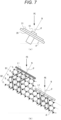
- Fig. 7 illustrates a schematic view of the method for evaluating a SiC substrate described in Patent Literatures 1 and 2.
- Fig. 7(a) illustrates a state in which a SiC substrate 10 to be evaluated is installed on a stage 20 of a scanning electron microscope.
- Fig. 7(b) illustrates a crystal structure of a surface of the SiC substrate 10.
- the image is acquired by making an electron beam PE incident on the SiC substrate 10 at an incident angle ⁇ inclined by 30° to 40° with respect to a normal line N of the ⁇ 0001 ⁇ plane of the SiC substrate 10.
- Cost reduction is one of urgent issues in spreading SiC semiconductor devices. As with the development of Si semiconductor devices, the cost reduction largely depends on an increase in diameter of a semiconductor substrate. This is because a substrate (wafer) having a larger area can increase the number of semiconductor chips obtained from one substrate, so that a manufacturing cost per chip can be reduced. Therefore, the importance of a method for evaluating a SiC substrate having a large diameter is increasing.
- the method for evaluating a SiC substrate described in Patent Literatures 1 and 2 also has a problem in that the electron beam PE is easily defocused when scanning the SiC substrate 10 having a large diameter.
- the stage 20 is inclined at 30° to 40° to acquire the image I. Therefore, it is necessary to precisely control the stage 20 so as not to cause the surface of the SiC substrate 10 to deviate from a focal position of the electron beam PE.
- Fig. 8 illustrates a schematic view illustrating a movement amount when the SiC substrate 10 is scanned.
- Fig. 8(a) illustrates a state in which the SiC substrate 10 having a small area is evaluated.
- Fig. 8(b) illustrates a state in which the SiC substrate 10 having a large area is evaluated.
- an object of the present invention is to provide a novel evaluation method suitable for evaluating a SiC substrate having a large diameter.
- the present invention is a method for evaluating a SiC substrate, the method including an image acquisition step of acquiring an image by making an electron beam incident at an incident angle inclined with respect to a normal line of a ⁇ 0001 ⁇ plane of a SiC substrate, the incident angle being 10° or less.
- the incident angle As described above, by setting the incident angle to 10° or less, it is possible to reduce a chamber accommodating the SiC substrate in size. In addition, when a SiC substrate having a large diameter is scanned, it is possible to suppress deviation of a surface of the SiC substrate from a focal position of the electron beam.
- a preferred mode of the present invention includes an oxide film removal step of removing an oxide film of the SiC substrate, and the image acquisition step is performed after the oxide film removal step.
- the image acquisition step is a step of acquiring the image with the SiC substrate being exposed to ambient air for a time length of 60 minutes or less after the oxide film removal step.
- the exposure time of the SiC substrate to the ambient air is 60 minutes or less, the information on the surface of the SiC substrate can be accurately acquired.
- the image includes a plurality of pieces of brightness information reflecting a stacking direction of atoms, the preferred mode including a brightness comparison step of comparing the brightness information.
- the image includes first brightness information reflecting a first stacking direction and second brightness information reflecting a second stacking direction, the preferred mode including the brightness comparison step of comparing the first brightness information with the second brightness information.
- the incident angle is inclined to a ⁇ 1-100> direction with respect to the normal line.
- an acceleration voltage of the electron beam is 1.0 kV or less.
- a diameter of the silicon carbide substrate is 4 inches or more.
- Fig. 1 is a schematic view of the method for evaluating a SiC substrate 10 according to the present invention.
- Fig. 1(a) illustrates a state in which the SiC substrate 10 to be evaluated is installed on a stage 20, and an electron beam PE is incident on the SiC substrate 10 at an incident angle ⁇ of 8°.
- Fig. 1(b) illustrates a crystal structure of a surface of the SiC substrate 10 of Fig. 1(a) .
- the method for evaluating a SiC substrate according to the present invention is characterized in that an image I is acquired by making the electron beam PE incident at the incident angle ⁇ of 10° or less with respect to a normal line N of a ⁇ 0001 ⁇ plane of the SiC substrate 10.
- the method for evaluating a SiC substrate includes an oxide film removal step of removing an oxide film on the surface of the SiC substrate 10, an image acquisition step of acquiring the image I by making the electron beam PE incident at the incident angle ⁇ inclined with respect to the normal line N of the ⁇ 0001 ⁇ plane of the SiC substrate 10, and a brightness comparison step of comparing brightness information L included in the image I.
- a diameter of the SiC substrate 10 is preferably 4 inches or more, more preferably 6 inches or more, and still more preferably 8 inches or more.
- the oxide film removal step is a step of removing the oxide film formed on the surface of the SiC substrate 10 to expose crystal structures of Si and C on the surface of the SiC substrate 10.
- a method for removing the oxide film a method of removing the oxide film by a solution of hydrogen fluoride (HF), ammonium fluoride (NH 4 F), or the like, and a method of removing the oxide film by dry etching or in a gas phase of plasma or the like can be adopted.
- the oxide film removal step includes an etching method and a crystal growth method of the SiC substrate 10. That is, no oxide film is formed on the surface of the SiC substrate 10 after etching or growth. Therefore, the etching method and the crystal growth method of the SiC substrate 10 can be reasonably adopted as the oxide film removal step.
- etching method examples include a hydrogen etching method using hydrogen gas as etching gas, and a Si-vapor etching (SiVE) method of performing heating under a Si atmosphere.
- Examples of the crystal growth method include a chemical vapor deposition (CVD) method, a physical vapor transport (PVT) method, and a metastable solvent epitaxy (MSE) method.
- CVD chemical vapor deposition
- PVT physical vapor transport
- MSE metastable solvent epitaxy
- the image acquisition step is a step of acquiring the image I by making the electron beam PE incident on the SiC substrate 10 at the incident angle ⁇ inclined with respect to the normal line N of the ⁇ 0001 ⁇ plane of the SiC substrate 10.
- the incident angle ⁇ is, the incident angle ⁇ is preferably 10° or less, more preferably 9° or less, and still more preferably 8° or less.
- the incident angle ⁇ is preferably 5° or more, more preferably 6° or more, still more preferably 7° or more, and still more preferably 8° or more.
- the image acquisition step includes an installation step of installing the SiC substrate 10 to be evaluated on the stage 20 of a scanning electron microscope, an inclination step of inclining the stage 20 at an inclination angle ⁇ where the electron beam PE is incident at the incident angle ⁇ of 10° or less with respect to the normal line N of the ⁇ 0001 ⁇ plane of the SiC substrate 10, and an electron beam irradiation step of irradiating the SiC substrate 10 with the electron beam PE to obtain the image I.
- the stage is preferably inclined such that the electron beam PE is inclined to a ⁇ 1-100> direction with respect to the normal line N of the SiC substrate 10.
- the incident angle ⁇ of the electron beam PE is preferably in a range between 5° and 10°, more preferably in a range between 7° and 9°, and still more preferably 8°.
- the irradiation with the electron beam PE is preferably performed at an acceleration voltage of 1.0 kV or less.
- the image I is created on the basis of electrons (reflected electrons) obtained when the electron beam PE (primary electrons) emitted by an electron emission unit of the scanning electron microscope is bounced back on the surface of the SiC substrate 10, or emitted after the electron beam PE interacts with the SiC substrate 10, and electrons (secondary electrons) generated during the interaction.
- a detector disposed in the scanning electron microscope detects the reflected electrons and/or the secondary electrons, and the image I is created on the basis of positional information of the SiC substrate 10 and the detection results of the respective electrons.
- the SiC substrate 10 is exposed to the ambient air for a time length of preferably 60 minutes or less, more preferably 50 minutes or less, still more preferably 40 minutes or less, and still more preferably 30 minutes or less after the oxide film removal step.
- the incident angle ⁇ is 10° or less
- the image I is more easily affected by the oxide film than in a conventional case where the incident angle ⁇ is 30° to 40°. Therefore, by performing measurement with the SiC substrate 10 being exposed to the ambient air for the time length of 60 minutes or less, the brightness information L of the image I becomes clear.
- the brightness comparison step is a step of comparing a plurality of pieces of the brightness information L reflected in the image I.
- the brightness information L is information regarding contrast reflecting a stacking direction of atoms. By comparing the plurality of pieces of brightness information L, it is possible to obtain information on the surface of the SiC substrate 10.
- the brightness comparison step is a step of comparing first brightness information L1 reflecting the stacking direction of atoms with second brightness information L2 capable of being compared with the first brightness information L1.
- the first brightness information L1 and the second brightness information L2 are contrasted to obtain the information regarding the contrast, whether the first brightness information L1 is white or black.
- Fig. 2 is an example of the image I obtained at the image acquisition step.
- the image I has the plurality of pieces of brightness information L reflecting the number of SiC unit layers and/or stacking directions of the SiC unit layers.
- the brightness information L has a plurality of variations depending on a combination of the number of SiC unit layers, and a first stacking direction D1 (a direction in which the Si atoms are stacked as A ⁇ B ⁇ C) and a second stacking direction D2 (a direction in which the Si atoms are stacked as C ⁇ B ⁇ A).
- Fig. 2 includes the first brightness information L1 reflecting a crystal structure in which two SiC unit layers are stacked in the first stacking direction D1 (a crystal structure in which the Si atoms are stacked as A ⁇ B ⁇ C), and the second brightness information L2 reflecting a crystal structure in which two SiC unit layers are stacked in the second stacking direction D2 (a crystal structure in which the Si atoms are stacked as C ⁇ B ⁇ A).
- FIGs. 1 and 2 illustrate the case where 4H-SiC has the two pieces of brightness information L
- 4H-SiC may have third brightness information L3 reflecting a crystal structure in which one SiC unit layer is stacked.
- the method for evaluating a SiC substrate according to the present invention can similarly evaluate any polytype in which the stacking direction is changed.
- the variation of the brightness information L is determined by a combination of three SiC unit layers, and a first stacking direction (a direction in which the Si atoms are stacked as A ⁇ B ⁇ C ⁇ A) and a second stacking direction (a direction in which the Si atoms are stacked as A ⁇ C ⁇ B ⁇ A).
- the electron beam PE is made incident at the incident angle ⁇ of 10° or less with respect to the normal line N of the ⁇ 0001 ⁇ plane of the SiC substrate 10. This makes it possible to reduce a measurement device in size.
- Fig. 3 is an explanatory view illustrating a movement amount of the SiC substrate 10 and the stage 20.
- Fig. 3(a) illustrates a state in which the SiC substrate 10 is scanned at the incident angle ⁇ of 30°, and corresponds to a conventional method for evaluating a SiC substrate.
- Fig. 3(b) illustrates a state in which the SiC substrate 10 is scanned at the incident angle ⁇ of 8°, and corresponds to the method for evaluating a SiC substrate according to the present invention.
- a range (two-dot chain line portion) in which the SiC substrate 10 moves is smaller in the method for evaluating a SiC substrate according to the present invention. That is, by setting the incident angle ⁇ to 10° or less, it is possible to reduce the size of a chamber accommodating the SiC substrate 10 and to reduce a device cost.
- the electron beam PE is made incident on the SiC substrate 10 at the incident angle ⁇ of 10° or less with respect to the normal line N of the ⁇ 0001 ⁇ plane of the SiC substrate 10.
- the wafer moves 7.62 cm in a height direction of the stage 20.
- the 6-inch wafer is scanned in a state of being inclined at 8°, the wafer moves 2.12 cm in the height direction of the stage 20.
- the SiC substrate 10 was evaluated under the following conditions.
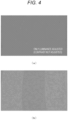
- Fig. 4(a) is the image I acquired at the image acquisition step according to Example 1.
- the SiC substrate 10 exposed to the ambient air for 60 minutes was measured at the incident angle ⁇ of 8°.
- the first brightness information L1 and the second brightness information L2 can be grasped. That is, information on the crystal structure of the outermost surface of the SiC substrate, information on a step shape, information on a step height, information on a distance to any place, and the like can be acquired from the image I acquired in Example 1.
- the SiC substrate 10 was evaluated under the following conditions.
- the SiC substrate 10 having the same conditions as those of Example 1 was used.
- the oxide film was removed under the same conditions as in Example 1.
- Fig. 4(b) is the image I acquired at the image acquisition step according to Example 2.
- the SiC substrate 10 exposed to the ambient air for 5 minutes was measured at the incident angle ⁇ of 8°.
- the first brightness information L1 and the second brightness information L2 can be grasped more clearly than in Example 1. That is, from the comparison between Example 1 and Example 2, it is found that the brightness information L can be accurately acquired by shortening the exposure time to the ambient air.
- Fig. 5 is a graph illustrating a relationship between the incident angle ⁇ and the contrast using the SiC substrate 10 of Example 2.
- the horizontal axis in Fig. 5 is the incident angle ⁇ of the electron beam PE with respect to the normal line N of the ⁇ 0001 ⁇ plane of the SiC substrate 10.
- the vertical axis in Fig. 5 is a value obtained by converting the contrast into numerical form by subtracting the second brightness information L2 (dark portion) from the first brightness information L1 (bright portion) on the image I.
- Fig. 5 shows that the contrast value is maximized at the incident angle ⁇ between 30° and 40° inclusive.
- the measurement is performed at the incident angle ⁇ between 30° and 40° inclusive, there arises problems that the measurement device becomes large and the electron beam PE is defocused at the time of measuring the SiC substrate 10 having a large diameter. Therefore, the inventors have found that the brightness information L can be obtained at the incident angle ⁇ of 10° or less as well.
- the present invention includes the image acquisition step of acquiring the image I by making the electron beam PE incident at the incident angle ⁇ inclined with respect to the normal line N of the ⁇ 0001 ⁇ plane of the SiC substrate 10, the incident angle ⁇ being 10° or less.
- the measurement chamber of the scanning electron microscope can be reduced in size as compared with the conventional case where the incident angle ⁇ is set to 30° to 40°.
- the present invention it is possible to suppress the deviation of the focal point at the time of measuring the substrate having a large diameter.
- the electron beam PE incident at the incident angle ⁇ smaller than that in the conventional method, it is possible to reduce the moving distance of the stage 20 in the irradiation direction of the electron beam PE when the SiC substrate 10 having a large diameter is scanned.
- the SiC substrate 10 having a large diameter is scanned, it is possible to suppress the deviation of the surface of the SiC substrate 10 from the focal position of the electron beam PE.
- the present invention also includes the oxide film removal step of removing the oxide film of the SiC substrate 10. As described above, by removing the oxide film formed on the SiC substrate 10, it is possible to acquire the brightness information L on the image I more clearly.
- the image acquisition step is a step of acquiring the image I with the SiC substrate 10 being exposed to the ambient air for the time length of 60 minutes or less after the oxide film removal step.
- the exposure time of the SiC substrate 10 to the ambient air is 60 minutes or less, the brightness information L on the image I can be acquired more clearly.
Landscapes
- Engineering & Computer Science (AREA)
- Physics & Mathematics (AREA)
- Life Sciences & Earth Sciences (AREA)
- Chemical & Material Sciences (AREA)
- Health & Medical Sciences (AREA)
- General Physics & Mathematics (AREA)
- Pathology (AREA)
- Analytical Chemistry (AREA)
- Biochemistry (AREA)
- General Health & Medical Sciences (AREA)
- Immunology (AREA)
- Medicinal Chemistry (AREA)
- Food Science & Technology (AREA)
- Quality & Reliability (AREA)
- Computer Vision & Pattern Recognition (AREA)
- Theoretical Computer Science (AREA)
- Analysing Materials By The Use Of Radiation (AREA)
- Length-Measuring Devices Using Wave Or Particle Radiation (AREA)
- Testing Or Measuring Of Semiconductors Or The Like (AREA)
Applications Claiming Priority (2)
| Application Number | Priority Date | Filing Date | Title |
|---|---|---|---|
| JP2020180970 | 2020-10-28 | ||
| PCT/JP2021/039698 WO2022092165A1 (ja) | 2020-10-28 | 2021-10-27 | 炭化ケイ素基板の評価方法 |
Publications (2)
| Publication Number | Publication Date |
|---|---|
| EP4239111A1 true EP4239111A1 (de) | 2023-09-06 |
| EP4239111A4 EP4239111A4 (de) | 2024-07-17 |
Family
ID=81381488
Family Applications (1)
| Application Number | Title | Priority Date | Filing Date |
|---|---|---|---|
| EP21886282.9A Pending EP4239111A4 (de) | 2020-10-28 | 2021-10-27 | Verfahren zur bewertung von siliciumcarbidsubstraten |
Country Status (6)
| Country | Link |
|---|---|
| US (1) | US12575380B2 (de) |
| EP (1) | EP4239111A4 (de) |
| JP (1) | JPWO2022092165A1 (de) |
| CN (1) | CN116391064A (de) |
| TW (1) | TW202232559A (de) |
| WO (1) | WO2022092165A1 (de) |
Family Cites Families (17)
| Publication number | Priority date | Publication date | Assignee | Title |
|---|---|---|---|---|
| US7164128B2 (en) * | 2003-11-25 | 2007-01-16 | Hitachi High-Technologies Corporation | Method and apparatus for observing a specimen |
| US20100215273A1 (en) * | 2005-06-24 | 2010-08-26 | Koninklijke Philips Electronics, N.V. | Methods and devices for characterizing polarization of illumination system |
| US20070081138A1 (en) * | 2005-10-11 | 2007-04-12 | Asml Netherlands B.V. | Lithographic projection apparatus, device manufacturing methods and mask for use in a device manufacturing method |
| US7221444B1 (en) * | 2005-10-14 | 2007-05-22 | 3I Systems Inc. | Method and system for improved defect sensitivity for inspecting surfaces |
| US8278739B2 (en) * | 2006-03-20 | 2012-10-02 | Semiconductor Energy Laboratory Co., Ltd. | Crystalline semiconductor film, semiconductor device, and method for manufacturing thereof |
| US7697128B2 (en) * | 2007-03-23 | 2010-04-13 | Asml Netherlands B.V. | Method of imaging radiation from an object on a detection device and an inspection device for inspecting an object |
| JP2010141124A (ja) * | 2008-12-11 | 2010-06-24 | Sumitomo Electric Ind Ltd | 基板および基板の製造方法 |
| JP2012255766A (ja) * | 2011-05-19 | 2012-12-27 | Elpida Memory Inc | 結晶材料の格子歪分布評価方法及び格子歪分布評価システム |
| CN104160520A (zh) * | 2012-02-01 | 2014-11-19 | 松下电器产业株式会社 | 半导体发光元件、其制造方法和光源装置 |
| JP6525189B2 (ja) | 2014-02-28 | 2019-06-05 | 学校法人関西学院 | 走査型電子顕微鏡用標準試料、その製造方法、走査型電子顕微鏡の評価方法、及びSiC基板の評価方法。 |
| KR102410666B1 (ko) * | 2015-01-09 | 2022-06-20 | 삼성전자주식회사 | 반도체 소자의 계측 방법, 및 이를 이용한 반도체 소자의 제조방법 |
| JP6708875B2 (ja) | 2016-04-27 | 2020-06-10 | 学校法人関西学院 | グラフェン前駆体付きSiC基板の製造方法及びSiC基板の表面処理方法 |
| JP6664133B2 (ja) | 2016-04-27 | 2020-03-13 | 学校法人関西学院 | 傾斜支持台付き標準試料、その製造方法、走査型電子顕微鏡の評価方法、及びSiC基板の評価方法 |
| JP2018188327A (ja) | 2017-05-01 | 2018-11-29 | 住友電気工業株式会社 | 炭化珪素基板の評価方法 |
| US11107655B2 (en) | 2017-09-20 | 2021-08-31 | Hitachi High-Technologies Corporation | Charged particle beam device |
| CN112513348B (zh) | 2018-07-25 | 2023-11-14 | 株式会社电装 | SiC晶片和SiC晶片的制造方法 |
| WO2021166035A1 (ja) * | 2020-02-17 | 2021-08-26 | 国立大学法人東北大学 | 位相イメージング用のx線発生装置 |
-
2021
- 2021-10-27 EP EP21886282.9A patent/EP4239111A4/de active Pending
- 2021-10-27 JP JP2022559208A patent/JPWO2022092165A1/ja active Pending
- 2021-10-27 CN CN202180069677.9A patent/CN116391064A/zh active Pending
- 2021-10-27 TW TW110139804A patent/TW202232559A/zh unknown
- 2021-10-27 WO PCT/JP2021/039698 patent/WO2022092165A1/ja not_active Ceased
- 2021-10-27 US US18/251,124 patent/US12575380B2/en active Active
Also Published As
| Publication number | Publication date |
|---|---|
| EP4239111A4 (de) | 2024-07-17 |
| US12575380B2 (en) | 2026-03-10 |
| CN116391064A (zh) | 2023-07-04 |
| WO2022092165A1 (ja) | 2022-05-05 |
| US20230411225A1 (en) | 2023-12-21 |
| TW202232559A (zh) | 2022-08-16 |
| JPWO2022092165A1 (de) | 2022-05-05 |
Similar Documents
| Publication | Publication Date | Title |
|---|---|---|
| CN110192266B (zh) | SiC外延晶片及其制造方法 | |
| CN109642342B (zh) | SiC外延晶片及其制造方法、以及缺陷识别方法 | |
| US7612334B2 (en) | Standard reference component for calibration, fabrication method for the same, and scanning electron microscope using the same | |
| US20220223482A1 (en) | EVALUATION METHOD AND MANUFACTURING METHOD OF SiC EPITAXIAL WAFER | |
| US10032600B2 (en) | Charged particle source | |
| US10274537B2 (en) | Test device for defect inspection | |
| Sakic et al. | High-efficiency silicon photodiode detector for sub-keV electron microscopy | |
| US11043356B2 (en) | Local alignment point calibration method in die inspection | |
| US8906727B2 (en) | Heteroepitaxial growth using ion implantation | |
| US12038388B2 (en) | Method for evaluating defect in monoclinic gallium oxide | |
| US20230055999A1 (en) | SiC EPITAXIAL WAFER, AND METHOD OF MANUFACTURING THE SAME | |
| US10985079B2 (en) | Method of manufacturing SiC epitaxial wafer | |
| US12575380B2 (en) | Evaluation method for silicon carbide substrates | |
| US20180219069A1 (en) | Silicon carbide single crystal, silicon carbide single crystal wafer, silicon carbide single crystal epitaxial wafer, and electronic device | |
| Kallinger et al. | Benchmarking experiment of substrate quality including SmartSiCTM wafers by epitaxy in a batch reactor | |
| Glaser et al. | Analysis of ALD dielectric leakage in bulk GaN MOS devices | |
| Moll | Polycrystalline Cubic Silicon Carbide Thin Films For MEMS | |
| EP4239112A1 (de) | Verfahren zur beurteilung der umgebung einer wärmebehandlung und siliciumcarbidsubstrat | |
| US20240297222A1 (en) | SiC EPITAXIAL WAFER | |
| Jazizadeh | Epitaxy, characterisation and microfabrication of tailor–made 3C–SiC/Si heterostructures for advanced technological semiconductors | |
| Kimoto et al. | Spatially-resolved EELS analysis of multilayer using EFTEM and STEM | |
| Baierhofer et al. | Defect Reduction in Epilayers for SiC Trench MOSFETs by Enhanced Epitaxial Growth | |
| US20260031300A1 (en) | Standard sample for use in transmission electron microscope, method of preparing the same, method of adjusting transmission electron microscope, and method of analyzing observation image obtained with transmission electron microscope | |
| Mangu | Pixelated GaSb Membranes for Photovoltaics: Fabrication and Structure-Property Relationships | |
| Tseng | A Study on the Relationship Between Defect Density, Doping Concentration, and Electrical Properties of 4H-SiC |
Legal Events
| Date | Code | Title | Description |
|---|---|---|---|
| STAA | Information on the status of an ep patent application or granted ep patent |
Free format text: STATUS: THE INTERNATIONAL PUBLICATION HAS BEEN MADE |
|
| PUAI | Public reference made under article 153(3) epc to a published international application that has entered the european phase |
Free format text: ORIGINAL CODE: 0009012 |
|
| STAA | Information on the status of an ep patent application or granted ep patent |
Free format text: STATUS: REQUEST FOR EXAMINATION WAS MADE |
|
| 17P | Request for examination filed |
Effective date: 20230329 |
|
| AK | Designated contracting states |
Kind code of ref document: A1 Designated state(s): AL AT BE BG CH CY CZ DE DK EE ES FI FR GB GR HR HU IE IS IT LI LT LU LV MC MK MT NL NO PL PT RO RS SE SI SK SM TR |
|
| DAV | Request for validation of the european patent (deleted) | ||
| DAX | Request for extension of the european patent (deleted) | ||
| REG | Reference to a national code |
Ref country code: DE Ref legal event code: R079 Free format text: PREVIOUS MAIN CLASS: C30B0029360000 Ipc: G01N0023225100 |
|
| A4 | Supplementary search report drawn up and despatched |
Effective date: 20240617 |
|
| RIC1 | Information provided on ipc code assigned before grant |
Ipc: H01L 21/02 20060101ALN20240611BHEP Ipc: G01N 33/38 20060101ALN20240611BHEP Ipc: G01N 23/2202 20180101ALN20240611BHEP Ipc: H01L 21/66 20060101ALI20240611BHEP Ipc: G06T 7/00 20170101ALI20240611BHEP Ipc: G01N 33/00 20060101ALI20240611BHEP Ipc: G01N 23/2251 20180101AFI20240611BHEP |