EP4239960A1 - Système de traitement, circuit intégré associé, système et procédé - Google Patents
Système de traitement, circuit intégré associé, système et procédé Download PDFInfo
- Publication number
- EP4239960A1 EP4239960A1 EP23156362.8A EP23156362A EP4239960A1 EP 4239960 A1 EP4239960 A1 EP 4239960A1 EP 23156362 A EP23156362 A EP 23156362A EP 4239960 A1 EP4239960 A1 EP 4239960A1
- Authority
- EP
- European Patent Office
- Prior art keywords
- signal
- cnt
- circuit
- processing system
- count value
- Prior art date
- Legal status (The legal status is an assumption and is not a legal conclusion. Google has not performed a legal analysis and makes no representation as to the accuracy of the status listed.)
- Withdrawn
Links
Images


Classifications
-
- G—PHYSICS
- G06—COMPUTING OR CALCULATING; COUNTING
- G06F—ELECTRIC DIGITAL DATA PROCESSING
- G06F13/00—Interconnection of, or transfer of information or other signals between, memories, input/output devices or central processing units
- G06F13/38—Information transfer, e.g. on bus
- G06F13/382—Information transfer, e.g. on bus using universal interface adapter
- G06F13/385—Information transfer, e.g. on bus using universal interface adapter for adaptation of a particular data processing system to different peripheral devices
-
- H—ELECTRICITY
- H04—ELECTRIC COMMUNICATION TECHNIQUE
- H04L—TRANSMISSION OF DIGITAL INFORMATION, e.g. TELEGRAPHIC COMMUNICATION
- H04L25/00—Baseband systems
- H04L25/02—Details ; arrangements for supplying electrical power along data transmission lines
- H04L25/0262—Arrangements for detecting the data rate of an incoming signal
-
- G—PHYSICS
- G06—COMPUTING OR CALCULATING; COUNTING
- G06F—ELECTRIC DIGITAL DATA PROCESSING
- G06F13/00—Interconnection of, or transfer of information or other signals between, memories, input/output devices or central processing units
- G06F13/38—Information transfer, e.g. on bus
- G06F13/42—Bus transfer protocol, e.g. handshake; Synchronisation
- G06F13/4282—Bus transfer protocol, e.g. handshake; Synchronisation on a serial bus, e.g. I2C bus, SPI bus
- G06F13/4291—Bus transfer protocol, e.g. handshake; Synchronisation on a serial bus, e.g. I2C bus, SPI bus using a clocked protocol
-
- G—PHYSICS
- G06—COMPUTING OR CALCULATING; COUNTING
- G06F—ELECTRIC DIGITAL DATA PROCESSING
- G06F8/00—Arrangements for software engineering
- G06F8/60—Software deployment
- G06F8/65—Updates
Definitions
- Embodiments of the present disclosure relate to a microcontroller comprising a Universal Asynchronous Receiver-Transmitter (UART).
- UART Universal Asynchronous Receiver-Transmitter
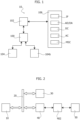
- Figure 1 shows a block diagram of an exemplary digital processing system 10, in particular a microcontroller.
- the processing system 10 comprises a microprocessor 102, usually the Central Processing Unit (CPU), programmed via software instructions.
- the software executed by the microprocessor 102 is stored in a non-volatile program memory 104, such as a Flash memory or EEPROM.
- the memory 104 is configured to store the firmware of the processing unit 102, wherein the firmware includes the software instructions to be executed by the microprocessor 102.
- the non-volatile memory 104 may also be used to store other data, such as configuration data, e.g., calibration data.
- the microprocessor 102 usually has associated also a volatile memory 104b, such as a Random-Access-Memory (RAM).
- RAM Random-Access-Memory
- the memory 104b may be used to store temporary data.
- the communication with the memories 104 and/or 104b is performed via one or more memory controllers 100.
- the memory controller(s) 100 may be integrated in the microprocessor 102 or connected to the microprocessor 102 via a communication channel, such as a system bus of the processing system 10.
- the system bus may comprise one or more bus systems, e.g., based on the Advanced eXtensible Interface (AXI) bus architecture, and/or a Network-on-Chip (NoC).
- AXI Advanced eXtensible Interface
- NoC Network-on-Chip
- the memories 104 and/or 104b may be integrated with the microprocessor 102 in a single integrated circuit, or the memories 104 and/or 104b may be in the form of a separate integrated circuit and connected to the microprocessor 102, e.g., via the traces of a printed circuit board.
- the microprocessor 102 may have associated one or more (hardware) resources/peripherals 106 selected from the group of
- the system bus may indeed comprise an Advanced Microcontroller Bus Architecture (AMBA) High-performance Bus (AHB), and an Advanced Peripheral Bus (APB) used to connect the resources/peripherals 106 to the AMBA AHB bus.
- AMBA Advanced Microcontroller Bus Architecture
- AHB Advanced Peripheral Bus
- the digital processing system 10 may support different functionalities.
- the behavior of the microprocessor 102 is determined by the firmware stored in the memory 104, e.g., the software instructions to be executed by a microprocessor 102 of a micro-controller 10.
- the firmware stored in the memory 104
- the processing system 10 may receive a new firmware from a detachable program/diagnostic tool 30, e.g., used in a service center, and/or another processing system 40.
- a detachable program/diagnostic tool 30 e.g., used in a service center
- another processing system 40 may be connected to the processing system 10 to be updated in any suitable manner, such as a communication system 20.
- the processing system 40 may be configured to exchange data with one or more remote servers 50 via one or more wireless communication modules 402.
- a processing system 40 is often used to provide status and/or diagnostic information to the server 50.
- the processing system 40 may also receive the new firmware for a given processing system 10 via the communication interface 402 from a remote server 50.
- the communication interface 402 and the remote server(s) 50 may exchange data via Internet.
- Figure 3 shows an example of a firmware update procedure.
- the update procedure may be activated once the product incorporating the processing system 10 has been delivered.
- the update procedure may be handled by a dedicated hardware resource of the processing system and/or by a suitable programming of the processing unit 102.
- the processing unit 102 may also be switched off during the update procedure.
- the processing unit 102 execute a given firmware containing also the update function.
- this firmware may be directly the old firmware of the processing system 10, i.e., the old firmware contains instructions for implementing the update procedure.
- the update function may be implemented in a separate firmware image, such as a separate system firmware. For example, once having received an update request, the processing system 10 may activate such a separate firmware image in order to handle the update request.
- the processing system 10 receives at a step 1002 a new firmware via a communication interface of the processing systems 10 and stores at a step 1006 the firmware received to the program memory 104 of the processing system.
- the program memory 104 is often split into a plurality of updateable firmware memory areas, e . g ., two memory areas, wherein a respective firmware image may be stored to each updateable firmware memory area at the step 1006.
- the old firmware (currently used by the processing system 10) may thus be stored to a first memory area, and the processing systems 10 is configured to store the new firmware received to a second memory area, i . e ., without overwriting the old firmware.
- the processing system 10 may validate at a step 1004 the firmware received.
- the processing system 10 may receive an encrypted version of the firmware.
- the processing system 10 may validate the firmware by verifying whether (at least part of) the firmware received may be decrypted.
- the processing system 10 may either store the decrypted or encrypted version to the memory 104.
- the encrypted version may be stored when the memory controller 100 of the memory 104 supports also a real-time decryption operating of the firmware read from the program memory 104.
- the processing system 10 may stores at a step 1008 firmware identification data to a non-volatile memory in order to indicate, which updateable firmware image should be used.
- this memory may be any non-volatile memory of the processing system 10, including the program memory 104 or a further non-volatile memory.
- the processing system 10 may read the firmware identification data, decide which updateable firmware image should be used and execute the respective firmware image.
- the firmware of the processing system 10 may be updated via a debug interface, such as a JTAG (Joint Test Action Group) interface, which, e . g ., may be used to write directly data to the non-volatile memory 104.
- a debug interface such as a JTAG (Joint Test Action Group) interface, which, e . g ., may be used to write directly data to the non-volatile memory 104.
- the communication system 20 is also based on an UART communication.
- the processing system 10 may comprise an UART communication interface and the microprocessor 102 or a dedicated hardware circuit may be configured to receive the firmware via the UART communication interface.
- UART-JTAG converter circuits configured to convert a communication exchanged via a UART into a communication used to interface a JTAG interface.
- UART-JTAG converter circuit may be integrated directly within the integrated circuit of the processing system 10 or within a separate integrated circuit, which is connected to a JTAG interface of the processing system 10, e.g., via traces of an integrated circuit board.
- UART uses two separate signals: a transmission signal TX and a reception signal RX, i.e., an UART interface is configured to generate a transmission signal TX and receive a reception signal. Accordingly, two UART interfaces may exchange data by connecting the transmission signal TX of a first UART interface to the reception signal RX of the second UART interface. Similarly, the transmission signal TX of the second UART interface is connected to the reception signal RX of the first UART interface.
- RS-232 Recommended Standard 232
- RS-485 Recommended Standard 485
- TIA-485(-A) or EIA-485 transceivers.
- UART is a serial asynchronous transmission protocol
- both the transmitter circuit, e.g., the circuit 30 or 40, and the receiver circuit, e.g., the circuit 10 use a given transmission velocity in order to exchange an UART frame.
- a typical UART interface is configured to send and receive fixed length UART frames comprising only a few data bits, such as 1 byte (8 bits) or 2 bytes (16 bits).
- a typical UART frame comprises moreover:
- a descriptor of the operation mode 8N1 indicates eight data bits (8), no parity (N) and one (1) stop bit are transmitted or received. Accordingly, UART frames have a fixed length of bits, e.g., 10 bits for the format 8N1 (including the start bits)
- the communication via such an UART interface is usually a low velocity communication.
- typical support baud rates are 9600, 14400, 19200, 38400, 57600 bits/s. This applies in particular when long cables are used for the UART communication between the processing system 10 and the detachable program tool 30 or the processing system 40, because such cables are affected by parasitic capacitances and inductances.
- the UART interface may be configured to use a fixed or predetermined baud rate.
- the transmission velocity is usually not optimized for the current application scenario, e . g ., because a higher baud rate could be used when the cable is shorted.
- one or more of the above objectives is achieved by means of a processing system having the features specifically set forth in the claims that follow.
- Embodiments moreover concern a related integrated circuit, system and method.
- the processing system comprises a transmission terminal configured to provide a transmission signal, a reception terminal configured to receive a reception signal and an UART communication interface.
- the UART communication interface comprises a clock management circuit configured to receive a clock signal and generate a down-scaled clock signal as a function of a clock scaling factor.
- a transmission circuit of the UART communication interface is configured to sequentially transmit, in response to the down-scaled clock signal, via the transmission signal a given number of bits stored to a transmission data register of the UART communication interface.
- a reception circuit is configured to sequentially receive, in response to the down-scaled clock signal, via the reception signal a given number of bits and store the received bits to a reception data register of the UART communication interface.
- the processing system comprises also a baud-rate detection circuit.
- the baud-rate detection circuit comprises a further clock management circuit, an edge detector, a digital counter circuit, a validation circuit and a register.
- the further clock management circuit is configured to receive the clock signal and generate a further clock signal.
- the edge detector is configured to generate a first control signal indicating rising and falling edges in the reception signal.
- the digital counter circuit is configured to monitor the first control signal, and in response to determining that the first control signal signals an edge in the reception signal, reset a count value. Conversely, in response to determining that the first control signal does not signal an edge in the reception signal, the digital counter increases the count value in response to the further clock signal.
- the validation circuit is configured to monitor the first control signal and the count value. In response to determining that the first control signal signals an edge in the reception signal and when the count value is smaller than a maximum value, the validation circuit asserts a second control signal. Conversely, in response to determining that the first control signal does not signal an edge in the reception signal or when the count value is equal to or greater than the maximum value, the validation circuit de-asserts the second control signal.
- the register is configured to provide a threshold signal by storing the count value when the second control signal is asserted, wherein the clock scaling factor is derived from the threshold signal.
- the clock management circuit comprises a first down-scaling circuit configured to generate the down-scaled clock signal via a first counter configured to increase a first count value in response to the clock signal until the first count value reaches a first threshold value.
- the first threshold value may correspond to the threshold signal stored to the register.
- the first down-scaling circuit is configured to generate a pre-scaled clock signal and the clock management circuit comprises also a second down-scaling circuit configured to receive the pre-scaled clock signal and generate the down-scaled clock signal as a function of a second clock scaling factor.
- the first threshold value of the first down-scaling circuit may be derived from the threshold signal, or the further clock management circuit may comprise a third down-scaling circuit configured to receive the clock signal and generate the further clock signal as a function of the second clock scaling factor.
- the baud rate of the UART communication interface in particularly the frequency of the down-scaled clock signal used by the transmission circuit and the reception circuit, is determined via the threshold signal stored to the register, wherein the register is update when the time between two consecutive edges of the reception signal is validated by the validation circuit.
- the maximum value (indicating a minimum permitted baud rate) may be selected in a range between a nominal count value and the double of the nominal count value, or may correspond to the double of the nominal count value.
- the nominal count value may be fixed or predetermined, or the nominal count value may correspond to the threshold signal, i.e., the baud-rate detection circuit may adapt the maximum value as a function of the threshold signal stored to the register.
- the validation circuit may also be configured to assert the second control signal only when the count value is also greater than a minimum value (indicating a maximum permitted baud rate).
- a minimum value may be selected in a range between the nominal count value and half of the nominal count value, or may correspond to half of the nominal count value. Accordingly, also in this case, when the nominal count value corresponds to the threshold signal, the baud-rate detection circuit may be configured to adapt the minimum value as a function of the threshold signal.
- the UART communication interface may be used to receive a firmware for a microcontroller.
- the processing system comprises thus also a microprocessor configured to execute software instructions, a non-volatile memory configured to store the software instructions, and a debug interface, such as a JTAG interface, configured to analyze the content of the reception data register in order to determine one or more debug command packets used to write new software instructions to the non-volatile memory.
- the debug interface is configured to store, in response to each debug command packet, a respective debug response packet to the transmission data register, thereby also signaling the correct reception of a debug command packet.
- an UART transmitter circuit may be configured to sequentially transmit according to a given baud rate data (e . g ., comprising a firmware) via the reception signal to the processing system, whereby the UART communication interface of the processing system automatically sets the frequency of the down-scaled clock signal used by the transmission circuit and the reception circuit, when the data are received.
- the UART transmitter circuit may be configured to vary the baud rate during the transmission of the data, e . g ., reduce the baud rate when the UART transmitter circuit does not receive the response packet from the processing system.
- FIG. 4 shows an embodiment of a processing system 10a in accordance with the present description.
- the processing system 10a comprises at least one processing core 102a, such as n processing cores 102a 1 ...102a n , connected to a (on-chip) communication system 114.
- the processing cores 102a 1 ...102a n may be ARM Cortex ® -R52 cores.
- the communication system 114 may comprise one or more bus systems, e.g., based on the Advanced eXtensible Interface (AXI) bus architecture, and/or a Network-on-Chip (NoC).
- AXI Advanced eXtensible Interface
- NoC Network-on-Chip
- each processing core 102a may comprise a microprocessor 1020 and a communication interface 1022 configured to manage the communication between the microprocessor 1020 and the communication system 114.
- the interface 1022 is a master interface configured to forward a (read or write) request from the microprocessor 1020 to the communication system 114, and forward an optional response from the communication system 114 to the microprocessor 1020.
- the processing core 102a may also comprise a slave interface 1024.
- a first microprocessor 1020 may send a request to a second microprocessor 1020 (via the communication interface 1022 of the first microprocessor, the communication system 114 and the communication interface 1024 of the second microprocessor).
- the communication system 114 may comprise in addition to a system bus or NoC, also an additional co-processor bus, e . g ., connecting the microprocessors 1020 of the same processing core 102a or all processing cores 102a.
- each processing core 102a 1 ...102a n may also comprise further local resources, such as one or more local memories 1026, usually identified as Tightly Coupled Memory (TCM).
- TCM Tightly Coupled Memory
- the processing cores 102a 1 ...102a n are arranged to exchange data with a non-volatile memory 104 and/or a volatile memory 104b.
- these memories are system memories, i . e ., shared for the processing cores 102a 1 ...102a n .
- the processing system 10a comprises one or more memory controllers 100 configured to connect at least one non-volatile memory 104 and at least one volatile memory 104b to the communication system 114.
- one or more of the memories 104 and/or 104b may be integrated in an integrated circuit 30a comprising the processing core(s) 102a or may be connected externally to the integrated circuit 30a.
- the non-volatile memory 104 may be used to store the firmware of one or more of the microprocessors 1020.
- the processing system 10a may comprise one or more resources 106, such as one or more communication interfaces or co-processors (e . g ., a cryptographic co-processor).
- the processing system 10a comprises a UART communication interface 50, which is preferably connected to the communication system 114 via a slave communication interface 504, such as a peripheral bridge.
- the UART communication interface 50 comprises a hardware transmission and reception interface circuit 506 configured to interface a UART communication channel by generating a transmission signal TX and receiving a reception signal RX.
- the UART communication interface 50 may also comprise one or more transmission data registers DATATX for storing data to be transmitted, one or more control registers CTRL for storing control data, and one or more reception data registers DATARX for storing data having been received.
- the same registers may be used as transmission data registers DATATX and reception data registers DATARX.
- the slave interface 504 may be used to interface these registers with the communication system 114.
- a processing core 102a may be configured to send one or more of the following requests via the communication system 114 to the slave interface 504 of the communication interface 50:
- each of the registers DATATX, DATARX and CTRL may have associated a respective physical address (PA) of the communication system 114, and each read or write request may comprise a given target address.
- the communication system 114 may comprise an Advanced Microcontroller Bus Architecture (AMBA) High-performance Bus (AHB), and an Advanced Peripheral Bus (APB) used to connect the communication interface 50 to the AMBA AHB bus.
- AMBA Advanced Microcontroller Bus Architecture
- AHB Advanced Peripheral Bus
- the UART interface 50 may also comprise a master interface 502, often also identified as integrated Direct-Memory-Access (DMA) controller.
- a master interface 502 may be useful in case the UART interface 50 has to start a communication in order to exchange data via (read and/or write) request with another circuit connected to the communication system 114, such as a memory 104/104b, a resource 106 or a processing core 102.
- the master interface/DMA controller 502 may be configured to generate write requests in order to store data received via the reception signal RX to the non-volatile memory 104, thereby storing a new firmware to the program memory 104.
- an optional debug interface 60 such as a JTAG interface.
- a debug interface 60 may be configured to read data from or write to one or more registers or memory locations of the processing system 10a.
- the debug interface 60 may comprise a master interface 602 configured to send read or write requests to the communication system 114 and/or an additional dedicated debug communication system.
- the debug interface 60 may also comprise a slave interface 604, which may be used, e.g., in order to program/configure whether the access to one or more of the registers and/or memory locations via the debug interface 60 is permitted or inhibited.
- the UART interface 50 may be configured to exchange data with the debug interface 60, which in turn may be configured to store data to the non-volatile memory 104.
- the debug interface 60 may manage different debug commands and/or access protections may be implemented, which do not permit that the UART interface may directly store data to the memory 104, but the debug interface 60 may update the firmware, e . g ., when the protections are disabled, or when the protections are enabled and given commands are provided to unlock the protection, e . g ., by providing a password via a debug command received via the UART interface 50.
- the debug interface 60 is configured to receive a debug command packet and optionally a debug data packets.
- a debug data packet has a dimension corresponding to the word size of the processing system 10a, such as 1, 2, 4 or 8 bytes, e . g ., 4 bytes in case of a 32-bit microprocessor 1020.
- a debug command packet has typically a plurality of bytes, such as 2, 4 or 8 bytes, in order to indicate a debug command.
- the debug command packet may indicate a read request or a write request, wherein one or more following debug data packets comprise the respective data.
- the data of a write request may also be included directly in the debug command packet, which thus could have a variable size.
- the debug interface 60 may thus also be configured to provide a debug (response) data packet to the UART interface 50 to be transmitted via the transmission signal TX.
- the debug interface 60 may also generate a debug response packet, which, e . g ., may be transmitted in response to each debug command packet in order to provide a respective status response, e . g ., indicating whether the data included in a write request have been stored to the respective address.
- the debug response packet may have 1 or 2 bytes.
- the data of a read request may also be included directly in the debug response packet, which thus could have a variable size.
- the debug command packet, the debug data packet and the debug response packet are exchanged with the UART communication interface 50, e.g., by reading data from the previously mentioned register DATARX and writing data to the previously mentioned register DATATX.
- the data exchange between the UART interface 50 and the debug interface 60 may be implemented in any suitable manner, such as via a direct connection, the master interface 502, and/or the master interface 602.
- the UART interface is thus configured to exchanges the respective data via UART frames with the communication channel 20, e.g., by transmitting the debug response packet or an optional debug data packet by transmitting one or more UART frames via the transmission signal TX and/or receiving a debug command packet or an optional debug data packet by receiving one or more UART frames via the reception signal RX.
- each UART frame has 8 data bits, e.g., by using a frame format 8N1.
- each debug command packet would be received via two consecutive UART frames.
- each debug command packet would be transmitted via a single UART frames.
- a general-purpose DMA controller 110 may comprises at least one functional channel connected to a resource 106, such as the UART interface 50 and/or the debug interface 60.
- a resource 106 associated with a given channel may also be selected as a function of configuration data.
- a channel is either a read or write channel (which also may programmable) and has typically associated configuration data, which indicate the memory address-range from which the DMA controller 110 should read data or the memory address-range to which the DMA controller 110 should write data.
- a resource 106 may be connected to the DMA controller 110 via two channels:
- a general-purpose DMA controller 110 typically has associate a master interface 1102 for transmitting the read or write requests to the memory controller 100.
- the master interface 1102 may be connected via a dedicated DMA channel directly to the memory controller 110 or the master interface 1102 may send the requests to the communication system 114.
- the read and write requests may comprise any address managed by the communication system 114.
- a general-purpose DMA controller 110 may also be configured to exchange the data with the resource 106 via the communication system 114.
- the DMA controller 110 may be configured to send via the master interface 1102 first a read request comprising a first address and then a write request comprising a second address.
- a general-purpose DMA controller 110 may be used instead of the master interfaces 502 and/or 602. Moreover, typically a general-purpose DMA controller 110 comprises also a slave interface 1104 for receiving configuration data for configuring the DMA controller 110.
- FIG. 5 shows an embodiment of a hardware serial communication interface 506 of the UART interface 50.
- the hardware communication interface 506 comprises two shift registers 5060 and 5062.
- the shift register 5060 is used to store the data to be transmitted. Accordingly, once a data transmission is requested, the hardware communication interface 506 may transfer the content of the transmission data registers DATATX to the shift register 5060, e.g., by using a parallel data input PDI of the shift register 5060.
- the transmission data register DATATX and the shift-register 5060 have preferably the same dimension and are configured to store the data bits and the optional parity bits of one UART frame, such as 1 byte.
- the UART frame stored to the transmission data register DATATX may comprise or not comprise the start bit of the UART frame.
- a first bit of the shift-register 5060 may be set to "0", while the other bits of the shift-register 5060 are mapped to respective bits of the transmission data register DATATX.
- the transmission data register DATATX may comprise or not comprise the one or more stop bits of the UART frame.
- the data register DATATX and the shift-register 5060 may be implemented with the same shift-register, which may be written, e . g ., via the slave interface 504 and/or a DMA channel (circuits 502, 602 and/or 110).
- the shift register 5060 is configured to sequentially transmit the bits stored to the shift register 5060 as a function of a clock signal CLK 2 and a transmission enable signal TX_EN.
- the hardware communication interface 506 comprises also a clock management circuit 5064 configured to generate the clock signal CLK 2 for the hardware communication interface 506 in response to a system clock signal CLK of the processing system 10a.
- the clock management circuit may comprise a clock pre-scaling circuit 5078 configured to generate a pre-scaled clock signal CLK PRE having a reduced frequency with respect to the frequency of the clock signal CLK, wherein the scaling factor may be programmable as a function of the configuration data stored to the control register(s) CTRL.
- the pre-scaling circuit 5078 may be implemented with a counter configured to increase a count value in response to the clock signal CLK, wherein the counter changes the logic level of the clock signal CLK PRE when the count value reaches a threshold value BAUD_THR, wherein the threshold value BAUD_THR is determined as a function of the configuration data provided by the control register(s) CTRL.
- the pre-scaled clock signal CLK PRE is then provided to a further and optional down-scaling circuit 5080 configured to generate the clock signal CLK 2 having a reduce frequency with respect to the frequency of the clock signal CLK PRE , wherein the scaling factor may be fixed or programmable as a function of the configuration data stored to the control register(s) CTRL.
- the down-scaling circuit 5080 may be implemented with a counter configured to increase a count value in response to the clock signal CLK PRE , wherein the counter changes the logic level of the clock signal CLK PRE when the count value reaches a threshold value, wherein the threshold value is optionally determined as a function of the configuration data provided by the configuration register(s) CTRL.
- the operation of the down-scaling circuit 5080 is changed in response to a synchronization signal SYNC, which is however only used when receiving data and will be described later on.
- the clock signal CLK 2 corresponds to a down-scaled version of the clock signal CLK (as a function of the threshold BAUD_THR).
- the shift register 5060 also receives an enable signal TX_EN, which enables the data transmission operation.
- the shift register 5060 is configured to, when the enable signal TX_EN is asserted and in response to the clock signal CLK 2 , sequentially provide at a serial data output SDO the content of the shift-register 5060. Accordingly, when the enable signal TX_EN is asserted, the shift register 5060 sequentially provides the bits of the data stored to the shift register 5060.
- the enable signal TX_EN is generated by a transmission control circuit 5066 configured to determine whether a given number of requested bits has been transmitted. For example, the number of bits may be fixed or determined as a function of the UART frame format.
- the number of bits may correspond to 10 for the format 8N1.
- the transmission control circuit 5066 may also be configured to determine the number of requests bits to be transmitted as a function of the configuration data stored to the control register(s) CTRL, which, e.g., may indicate the number of parity bits and/or stop bits.
- the transmission control circuit 5066 may comprise a counter, which is increased in response to the clock signal CLK 2 , thereby indicating the number of transmitted bits. Accordingly, the counter may be reset when starting a new data transmission operation, thereby asserting the enable signal TX_EN, and the transmission control circuit 5066 de-asserts the enable signal TX_EN when the requested number of bits has been transmitted. For example, in this case, the transmission control circuit may assert a control/interrupt signal TX_OK when the transmission control circuit 5066 de-asserts the enable signal TX_EN.
- the hardware communication interface 506 comprises a combinational logic circuit 5070 configured to set the signal TX to high, when the enable signal TX_EN is de-asserted.
- the combinational logic circuit 5070 may be implemented with a logic OR gate receiving at input the serial data output signal SDO of the shift register 5076 and the inverted version of the enable signal TX_EN, and providing at output the signal TX.
- the combinational logic circuit 5070 is purely optional, because the serial data output signal SDO may also be set to high, when the enable signal TX_EN is de-asserted, e.g., because a stop bit is stored to the register 5060.
- the shift register 5062 is configured to store the bits received via the signal RX. Specifically, when no data transmission occurs, the reception signal RX is set to high. Once a transmission is started by another device, the start bit is transmitted, whereby the reception signal RX is set to low.
- the hardware communication interface 506 comprises a reception control circuit 5068. Specifically, the reception control circuit 5068 is configured to assert a reception enable signal RX_EN in response to a change of the signal RX from high to low, e.g., in response to a falling edge of the signal RX.
- the reception control circuit 5068 may use a counter, which is reset in response to detecting the start bit and increased in response to the clock signal CLK 2 , wherein the reception control circuit 5068 de-asserts the enable signal RX_EN when the requested number of bits has been received.
- the reception control circuit may assert a control/interrupt signal RX_OK when the reception control circuit 5068 de-asserts the enable signal RX_EN.
- the shift register 5062 is configured to, when the enable signal RX_EN is asserted and in response to the clock signal CLK 2 , sequentially add to the data stored to the shift register 5062 the logic level applied to a serial data input SDI of the shift register 5062, wherein the serial data input SDI is connected to the reception signal RX.
- the reception control circuit 5068 may assert the reception enable signal RX_EN with the start bit or only for the next bit, whereby the start bit is stored or not stored to the shift register 5062.
- the hardware communication interface 506 transfers the content of the shift register 5062 to the reception data register DATARX, e . g ., by using a parallel data output PDO of the shift register 5062.
- the reception data register DATARX and the shift-register 5062 have preferably the same dimension.
- the data register DATARX and the shift-register 5062 may be implemented with the same shift-register, which may be read, e . g ., via the slave interface 504 and/or a DMA channel (circuits 502, 602 and/or 110).
- Figure 7 shows in this respect a modified hardware communication interface 506, which comprises only a single shift register 5076. Accordingly, in the following will only be evidenced the differences with respect to Figure 5 .
- the shift register 5076 is configured to, when an enable signal EN is asserted, sequentially shift the content of the shift register 5076 in response to the clock signal CLK 2 , wherein a first bit is provided via a serial data output SDO of the shift register 5076 and a second bit received via a serial data input SDI of the shift register 5076 is added to the content of the shift register 5076.
- the serial data output SDO may be connected to the transmission signal TX, or preferably to the logic gate 5070.
- the serial data input SDI may be connected to the reception signal RX.
- the serial data input SDI may be connected to an additional logic gate 5072, which sets a signal RX' provided to the serial data input SDI to high, when the reception enable signal RX_EN is set to low.
- the logic gate 5072 is an OR gate receiving at input the reception signal RX and the inverted version of the reception enable signal RX_EN.
- the logic gate 5072 may also be used in the arrangement of Figure 5 .
- the enable signal EN of the shift register 5076 is asserted when either the transmission enable signal TX_EN or the reception enable signal RX_EN is asserted.
- the hardware communication interface 506 comprises a logic gate 5074, such as an OR gate, configured to generate the enable signal EN by combining the transmission enable signal TX_EN and the reception enable signal RX_EN.
- the transmission frame (with or without the start bit) may be transferred to the shift register 5076, either directly or indirectly via the transmission data register DATATX, e . g ., by using a parallel data input PDI of the shift register 5076.
- the reception frame (with or without the start bit) may be transferred from the shift register 5076, either directly or indirectly via the reception data register DATARX, e . g ., by using a parallel data output PDO of the shift register 5076.
- the transmission of data occurs in response to the clock signal CLK 2 , and the data are shifted out synchronously with this clock CLK 2 .
- the data received via the reception signal RX may have a phase and/or a frequency deviation from this clock CLK 2 .
- a frequency deviation leads to accumulated phase shifts, i.e., a frequency deviation can be viewed as a sequence of phase shifts.
- the reception control circuit 5068 may be configured to adjust the sampling point of the received data based on detected bit transitions. Specifically, in various embodiments, is used for this purpose the synchronization signal SYNC.
- the reception control circuit 5068 is configured to assert the synchronization signal SYNC in response to detecting a change of the logic level of the reception signal RX, i.e., in response to a falling edge and/or a rising edge of the signal RX.
- the reception control circuit 5068 may sample the reception signal RX in response to the clock signal CLK PRE and assert the synchronization signal SYNC when a current sample is set to high and the previous sample is set to low and/or when a current sample is set to the low and the previous sample is set to high.
- the down-scaling circuit 5080 may be synchronized with the synchronization signal SYNC in order to generate the edge used to sample the reception signal RX.
- the down-scaling circuit 5080 is implemented with a counter configured to increase a count value CNT, and reset the count value CNT when a maximum count value is reached.
- the counter CNT may be reset in response to determining that the synchronization signal SYNC is asserted.
- the logic level of the synchronization signal SYNC may be used to determine the increase value of the counter. For example, by default the increase value may be set to 1. Conversely, when the signal SYNC is asserted when the count value is set to 0, the increase value of the counter may be set to zero, whereby the phase "0" is repeated twice. Conversely, when the signal SYNC is asserted when the count value has its maximum value minus 1 ( e . g ., 3), the increase value of the counter may be set to two, whereby the counter is reset indirectly.
- the clock signal CLK PRE (or another clock signal) may also be used to perform an oversampling of the received signal RX (or RX').
- the hardware communication interface 506 comprises an oversampling circuit 5076, e . g ., comprising a shift register having a plurality of bits, wherein the oversampling circuit 5076 stores a plurality of subsequent values of the reception signal RX (or RX'), and then generates the signal provided to the serial data input SDI of the register 5076 (or similarly the register 5062) based on the stored values.
- the oversampling circuit 5076 stores an odd number of bits, such as three, and the signal provided to the serial data input SDI of the register 5076 is corresponds to the logic value of the majority of bits.
- the data transmission rate is defined via the threshold/signal BAUD_THR which specifies the threshold for the clock down-scaling circuit 5078.
- the UART interface may use a clock signal CLK 2 with 9600 Hz.
- two circuits connected via respective UART interfaces are configured to determine an optimized baud rate.
- the receiver circuit uses this frequency in order to (over) sample the received symbol, wherein the received bit sequence indicates whether the symbol has been transmitted with a baud rate BAUDRATE corresponding to a fraction of the maximum baud MAX_BAUDRATE rate.
- the microcontroller may sample the reception signal RX with 115,200 Hz and select the following baud rate:
- the UART interface 50 comprises or at least has associated a baud rate detection circuit 70 configured to set the frequency of the clock signal CLK 2 of the hardware transmission and reception interface circuit 506.
- Figure 8 shows an embodiment of the baud rate detection circuit 70.
- the baud rate detection circuit 70 uses a clock signal CLK 1 , which is derived from the clock signal CLK.
- the clock signal CLK 1 may correspond to the clock signal CLK or correspond to a frequency down-scaled version of the clock signal CLK.
- CLK 1 may correspond to the clock signal CLK or correspond to a frequency down-scaled version of the clock signal CLK.
- the reception signal RX is provided to an edge detector 700.
- this edge detector 700 may also correspond to the edge detector of the reception control circuit 5086.
- the baud rate detection circuit 70 could also be implemented directly within the reception control circuit 5068.
- the edge detector 700 generates a signal TRIG, such as a trigger signal, used to signal rising and falling edges in the reception signal RX.
- a signal TRIG such as a trigger signal
- the edge detector 700 may generate a pulse in the trigger signal TRIG, e . g ., by asserting the signal TRIG for a clock cycle of the clock signal CLK 1 , in response to detecting an edge in the reception signal RX (see also the respective description of the edge detector of the reception control circuit 5068).
- the signal TRIG is provided to a digital counter circuit 702.
- the counter circuit 702 is configured to reset a count value CNT when the signal TRIG signals an edge in the reception signal RX, e . g ., when the signal TRIG is asserted, and increase the count value CNT (typically by one) based on the clock signal CLK 1 (typically in response to a rising or falling edge of the clock signal CLK 1 ) when the signal TRIG does not signal an edge in the reception signal RX, e . g ., when the signal TRIG is de-asserted.
- the counter 702 may also use a maximum count value MAX_CNT, i.e., the counter 702 is configured to increase the count value CNT until the maximum count value MAX_CNT is reached or the signal the signal TRIG signals an edge in the reception signal RX.
- the count value CNT and the signal TRIG are provided to a validation circuit 704.
- the validation circuit 704 is configured to determine whether the count value CNT is in a given range. For example, in various embodiments, the validation circuit 704 may determine whether the count value CNT is smaller than a maximum count value, e . g ., corresponding to the previously mentioned value MAX_CNT. Generally, the validation circuit 704 may also determine whether the count value CNT is greater than a minimum count value MIN_CNT, wherein the value MIN_CNT is smaller than the value MAX_CNT.
- the validation circuit 704 in response to determining that the count value CNT is in the given permitted range, e . g ., smaller than the maximum count value MAX_CNT, the validation circuit 704 asserts a control signal SEL. Conversely, in response to determining that the count value CNT is not in the given permitted range, e . g ., greater than the maximum count value MAX_CNT, the validation circuit 704 de-asserts the control signal SEL.
- control signal SEL is provided to a register 708, which is configured to provide a signal BIT_CNT by storing the count value CNT in response to the clock signal CLK 1 (or also the clock signal CLK) when the control signal SEL is asserted.
- control signal SEL may be provided to a multiplexer 706 configured to receive at input the count value CNT and the signal BIT_CNT, wherein the multiplexer 706 provides at output the count value CNT when the control signal SEL is asserted.
- the baud rate detection circuit 70 is configured to generate a signal BIT_CNT indicative of the number of clock cycles of the clock signal CLK 1 between two consecutive edges of the reception signal RX.
- the baud rate detection circuit 70 automatically adapts the signal BIT_CNT based on the actual bit-time.
- the threshold value BAUD_THR for the clock scaling circuit 5078 may be derived from the signal BIT_CNT. Specifically, by using a down-scaling circuit 710 having the same scaling factor as the down-scaling circuit 5080 (when used), the signal BIT_CNT may directly be used as threshold value BAUD_THR. However, in case the down-scaling circuit 710 is omitted or has a different same scaling factor than the down-scaling circuit 5080 (when used), the signal BIT_CNT may also be scaled in order to generate the threshold value BAUD_THR.
- the register 708 may correspond to respective bits of the control register CTRL of the UART interface 50 providing the signal BAUD_THR.
- a flag of the control register CTRL may indicate whether the signal BAUD_THR should be provided by the control register CTRL or be derived from the signal BIT_CNT.
- the baud rate detection circuit 70 is configured to update the signal BIT_CNT only when the number of clock cycles CNT between two consecutive edges (as verified by the validation circuit 704) is in a given permitted range, in particular smaller than a maximum value MAX_CNT and optionally greater than a minimum value MIN_CNT.
- the transmitter circuit such as the circuits 30 or 40, is expected to transmit data with a given nominal baud rate NOM_BAUD, such as 19,200, which corresponds to a given nominal count value NOM_CNT of the counter 702 (based on the frequency of the clock signal CLK 1 ).
- NOM_BAUD nominal baud rate
- the bit time of a single bit would in this case be approximately 52 us (microseconds).
- the validation circuit 704 permits to verify whether the count value CNT indicates indeed the time of a single bit or a plurality of bits having the same logic value. In fact, the count value CNT would be the same for the following bit sequences:
- MAX_CNT NOM_COUNT x 2
- the transmitted circuit may vary the baud rate BAUD_RATE of the signal RX in the range between the minimum baud rate and the maximum baud rate, i.e., NOM BAUD/2 ⁇ BAUD RATE ⁇ NOMBAUD x 2. Accordingly, the baud rate BAUD_RATE may correspond to any permitted baud rate and not only the standard baud rates.
- the threshold value MAX_CNT and the threshold value MIN_CNT may also be derived from the signal BIT_CNT.
- the baud rate detection circuit 70 may comprise a circuit 712 configured to generate the signals MAX_CNT and optionally MIN_CNT via the following operations:
- the transmitter circuit may vary the used baud rate from the initial nominal value in order to increase or decrease the baud rate used during the data exchange with the processing system 10a.
- the baud rate of the communication of a given UART frame is in a range between the half and the double of the baud rate of the previous UART frame.
- the circuit 712 may also reset the values MAX_CNT and optionally MIN_CNT to the initial values calculated as a function of the nominal value NOM_COUNT when the edge detector 700 does not signal the reception of data for a given time period.
- the transmitter circuit 30 or 40 may thus transmit one or more (e . g ., debug) command packets with a given baud rate and verify whether the processing system 10a responds (within a given maximum time) with a respective ( e . g ., debug) response packet indicating that the communication is working correctly.
- the transmitter circuit may be configured to:
- the described baud rate detection and variation solutions may not only be used at the beginning of the communication, e.g., in order to set a highest possible baud rate, but the transmitter circuit may adapt the baud rate of the transmitted UART frames during the data transmission operation, i.e., in real-time, and the receiver circuit is able to dynamically adjust the baud rate used to receive the UART frames via the baud rate detection circuit 70.
- the communication is more robust, because in case of a missing response from the receiver circuit, the transmitter circuit may re-transmit the same (command or data) packet, while reducing on-the-fly the baud rate, until the receiver circuit again responds with a response packet, thereby avoiding that the communication is interrupted or even single packets are lost.
Landscapes
- Engineering & Computer Science (AREA)
- Theoretical Computer Science (AREA)
- General Engineering & Computer Science (AREA)
- Physics & Mathematics (AREA)
- General Physics & Mathematics (AREA)
- Power Engineering (AREA)
- Computer Networks & Wireless Communication (AREA)
- Signal Processing (AREA)
- Software Systems (AREA)
- Computer Security & Cryptography (AREA)
- Information Transfer Systems (AREA)
- Communication Control (AREA)
Applications Claiming Priority (1)
| Application Number | Priority Date | Filing Date | Title |
|---|---|---|---|
| IT202200004055 | 2022-03-03 |
Publications (1)
| Publication Number | Publication Date |
|---|---|
| EP4239960A1 true EP4239960A1 (fr) | 2023-09-06 |
Family
ID=81580671
Family Applications (1)
| Application Number | Title | Priority Date | Filing Date |
|---|---|---|---|
| EP23156362.8A Withdrawn EP4239960A1 (fr) | 2022-03-03 | 2023-02-13 | Système de traitement, circuit intégré associé, système et procédé |
Country Status (3)
| Country | Link |
|---|---|
| US (1) | US12056074B2 (fr) |
| EP (1) | EP4239960A1 (fr) |
| CN (1) | CN117251398A (fr) |
Cited By (1)
| Publication number | Priority date | Publication date | Assignee | Title |
|---|---|---|---|---|
| WO2025222871A1 (fr) * | 2024-04-23 | 2025-10-30 | 深圳市广和通无线股份有限公司 | Procédé et module d'adaptation de débit de communication en bauds, dispositif et support de stockage lisible |
Families Citing this family (1)
| Publication number | Priority date | Publication date | Assignee | Title |
|---|---|---|---|---|
| CN119938107B (zh) * | 2025-04-10 | 2025-07-04 | 深圳市斯帕克电气有限公司 | 一种烧写上位机的烧录管理方法和系统 |
Citations (3)
| Publication number | Priority date | Publication date | Assignee | Title |
|---|---|---|---|---|
| US6366610B1 (en) * | 1998-05-15 | 2002-04-02 | Advanced Micro Devices, Inc. | Autobauding with adjustment to a programmable baud rate |
| US20040062331A1 (en) * | 2002-09-27 | 2004-04-01 | Samuel Roshan J. | Self-tuning baud rate generator for UART applications |
| US20200319876A1 (en) | 2019-04-03 | 2020-10-08 | Stmicroelectronics Application Gmbh | Processing system, related integrated circuit, device and method |
Family Cites Families (5)
| Publication number | Priority date | Publication date | Assignee | Title |
|---|---|---|---|---|
| EP0666529B1 (fr) * | 1994-02-02 | 2004-10-06 | Advanced Micro Devices, Inc. | Gestion de l'énergie dans un émetteur/récepteur asynchrone |
| US5649122A (en) * | 1994-06-24 | 1997-07-15 | Startech Semiconductor, Inc. | Universal asynchronous receiver/transmitter with programmable xon/xoff characters |
| US5604870A (en) * | 1994-08-01 | 1997-02-18 | Moss; Barry | UART emulator card |
| WO2007125472A2 (fr) * | 2006-04-28 | 2007-11-08 | Nxp B.V. | Appareil de traitement de données |
| US11341015B2 (en) * | 2019-09-30 | 2022-05-24 | Texas Instruments Incorporated | UART receiver with adaptive sample timing control using a numerically-controlled oscillator |
-
2023
- 2023-02-13 EP EP23156362.8A patent/EP4239960A1/fr not_active Withdrawn
- 2023-03-03 CN CN202310195843.0A patent/CN117251398A/zh active Pending
- 2023-03-03 US US18/116,912 patent/US12056074B2/en active Active
Patent Citations (3)
| Publication number | Priority date | Publication date | Assignee | Title |
|---|---|---|---|---|
| US6366610B1 (en) * | 1998-05-15 | 2002-04-02 | Advanced Micro Devices, Inc. | Autobauding with adjustment to a programmable baud rate |
| US20040062331A1 (en) * | 2002-09-27 | 2004-04-01 | Samuel Roshan J. | Self-tuning baud rate generator for UART applications |
| US20200319876A1 (en) | 2019-04-03 | 2020-10-08 | Stmicroelectronics Application Gmbh | Processing system, related integrated circuit, device and method |
Cited By (1)
| Publication number | Priority date | Publication date | Assignee | Title |
|---|---|---|---|---|
| WO2025222871A1 (fr) * | 2024-04-23 | 2025-10-30 | 深圳市广和通无线股份有限公司 | Procédé et module d'adaptation de débit de communication en bauds, dispositif et support de stockage lisible |
Also Published As
| Publication number | Publication date |
|---|---|
| CN117251398A (zh) | 2023-12-19 |
| US20230281142A1 (en) | 2023-09-07 |
| US12056074B2 (en) | 2024-08-06 |
Similar Documents
| Publication | Publication Date | Title |
|---|---|---|
| EP4239960A1 (fr) | Système de traitement, circuit intégré associé, système et procédé | |
| TWI566546B (zh) | 用於檢查串聯式資料傳輸的修正過之功能的方法與裝置 | |
| EP3008610B1 (fr) | Bus d'extension d'interface de commande d'appareil photo | |
| Ziermann et al. | CAN+: A new backward-compatible Controller Area Network (CAN) protocol with up to 16× higher data rates. | |
| US20130343383A1 (en) | Method and device for a serial data transmission with additionally inserted data | |
| US9678828B2 (en) | Error detection capability over CCIe protocol | |
| EP4137954B1 (fr) | Système de traitement, circuit intégré associé, dispositif et méthode | |
| EP4138343B1 (fr) | Système de traitement, circuit intégré associé, dispositif et procédé | |
| US20100017654A1 (en) | Device-to-Device Communication Bus for Distributed Power Management | |
| US20150248373A1 (en) | Bit allocation over a shared bus to facilitate an error detection optimization | |
| KR20160140847A (ko) | 집적회로간 (i2c) 버스상에서 인-밴드로 여분의 정보를 전송하는 방법들 | |
| EP4116836A1 (fr) | Méthode de configuration de temps d'égalisation, puce et système de communication | |
| US20230205723A1 (en) | Communication device, communication method, and program | |
| CN107771331B (zh) | 独立式uark brk检测 | |
| US20020099451A1 (en) | Communication port control module for lighting systems | |
| TW201731272A (zh) | 具有自動從屬選擇產生之串列週邊介面 | |
| CN120104536B (zh) | 一种通道绑定方法、装置、设备、介质及程序产品 | |
| US20140333344A1 (en) | Adaptive interface for coupling fpga modules | |
| CN104486181A (zh) | 一种基于Modbus协议的从设备 | |
| JP6496747B2 (ja) | 通信するホストから離れた、シリアル半二重トランシーバにおけるtx/rxモード制御 | |
| US20070180173A1 (en) | Method and system for efficient framing on addressed buses | |
| US12411797B2 (en) | Interrupt latency and error resilient full-duplex SPI driver | |
| EP4224321B1 (fr) | Système de traitement, circuit intégré et procédé associés | |
| US5832302A (en) | Dual adder burst control governor to signal when a data burst is close to completion | |
| CN110554984A (zh) | 基于cpld的串口桥接方法及系统 |
Legal Events
| Date | Code | Title | Description |
|---|---|---|---|
| PUAI | Public reference made under article 153(3) epc to a published international application that has entered the european phase |
Free format text: ORIGINAL CODE: 0009012 |
|
| STAA | Information on the status of an ep patent application or granted ep patent |
Free format text: STATUS: THE APPLICATION HAS BEEN PUBLISHED |
|
| AK | Designated contracting states |
Kind code of ref document: A1 Designated state(s): AL AT BE BG CH CY CZ DE DK EE ES FI FR GB GR HR HU IE IS IT LI LT LU LV MC ME MK MT NL NO PL PT RO RS SE SI SK SM TR |
|
| STAA | Information on the status of an ep patent application or granted ep patent |
Free format text: STATUS: REQUEST FOR EXAMINATION WAS MADE |
|
| 17P | Request for examination filed |
Effective date: 20240226 |
|
| RBV | Designated contracting states (corrected) |
Designated state(s): AL AT BE BG CH CY CZ DE DK EE ES FI FR GB GR HR HU IE IS IT LI LT LU LV MC ME MK MT NL NO PL PT RO RS SE SI SK SM TR |
|
| STAA | Information on the status of an ep patent application or granted ep patent |
Free format text: STATUS: THE APPLICATION HAS BEEN WITHDRAWN |
|
| 18W | Application withdrawn |
Effective date: 20251201 |