EP4242596B1 - Sensoreinheit - Google Patents
Sensoreinheit Download PDFInfo
- Publication number
- EP4242596B1 EP4242596B1 EP22214452.9A EP22214452A EP4242596B1 EP 4242596 B1 EP4242596 B1 EP 4242596B1 EP 22214452 A EP22214452 A EP 22214452A EP 4242596 B1 EP4242596 B1 EP 4242596B1
- Authority
- EP
- European Patent Office
- Prior art keywords
- housing part
- circuit board
- printed circuit
- sensor unit
- unit
- Prior art date
- Legal status (The legal status is an assumption and is not a legal conclusion. Google has not performed a legal analysis and makes no representation as to the accuracy of the status listed.)
- Active
Links
Images

Classifications
-
- G—PHYSICS
- G01—MEASURING; TESTING
- G01D—MEASURING NOT SPECIALLY ADAPTED FOR A SPECIFIC VARIABLE; ARRANGEMENTS FOR MEASURING TWO OR MORE VARIABLES NOT COVERED IN A SINGLE OTHER SUBCLASS; TARIFF METERING APPARATUS; MEASURING OR TESTING NOT OTHERWISE PROVIDED FOR
- G01D11/00—Component parts of measuring arrangements not specially adapted for a specific variable
- G01D11/24—Housings ; Casings for instruments
- G01D11/245—Housings for sensors
-
- G—PHYSICS
- G01—MEASURING; TESTING
- G01C—MEASURING DISTANCES, LEVELS OR BEARINGS; SURVEYING; NAVIGATION; GYROSCOPIC INSTRUMENTS; PHOTOGRAMMETRY OR VIDEOGRAMMETRY
- G01C9/00—Measuring inclination, e.g. by clinometers, by levels
- G01C9/02—Details
- G01C9/06—Electric or photoelectric indication or reading means
-
- G—PHYSICS
- G01—MEASURING; TESTING
- G01D—MEASURING NOT SPECIALLY ADAPTED FOR A SPECIFIC VARIABLE; ARRANGEMENTS FOR MEASURING TWO OR MORE VARIABLES NOT COVERED IN A SINGLE OTHER SUBCLASS; TARIFF METERING APPARATUS; MEASURING OR TESTING NOT OTHERWISE PROVIDED FOR
- G01D11/00—Component parts of measuring arrangements not specially adapted for a specific variable
-
- G—PHYSICS
- G01—MEASURING; TESTING
- G01D—MEASURING NOT SPECIALLY ADAPTED FOR A SPECIFIC VARIABLE; ARRANGEMENTS FOR MEASURING TWO OR MORE VARIABLES NOT COVERED IN A SINGLE OTHER SUBCLASS; TARIFF METERING APPARATUS; MEASURING OR TESTING NOT OTHERWISE PROVIDED FOR
- G01D11/00—Component parts of measuring arrangements not specially adapted for a specific variable
- G01D11/24—Housings ; Casings for instruments
-
- G—PHYSICS
- G01—MEASURING; TESTING
- G01D—MEASURING NOT SPECIALLY ADAPTED FOR A SPECIFIC VARIABLE; ARRANGEMENTS FOR MEASURING TWO OR MORE VARIABLES NOT COVERED IN A SINGLE OTHER SUBCLASS; TARIFF METERING APPARATUS; MEASURING OR TESTING NOT OTHERWISE PROVIDED FOR
- G01D11/00—Component parts of measuring arrangements not specially adapted for a specific variable
- G01D11/24—Housings ; Casings for instruments
- G01D11/26—Windows; Cover glasses; Sealings therefor
-
- G—PHYSICS
- G01—MEASURING; TESTING
- G01D—MEASURING NOT SPECIALLY ADAPTED FOR A SPECIFIC VARIABLE; ARRANGEMENTS FOR MEASURING TWO OR MORE VARIABLES NOT COVERED IN A SINGLE OTHER SUBCLASS; TARIFF METERING APPARATUS; MEASURING OR TESTING NOT OTHERWISE PROVIDED FOR
- G01D7/00—Indicating measured values
Definitions
- the present invention relates to a sensor unit comprising an electronics unit, a first housing part and a second housing part connected thereto, wherein the electronics unit is connected to the first housing part and projects into the interior, wherein a contact region is provided which penetrates the first housing part, wherein the electronics unit has at least one printed circuit board with at least two printed circuit board sections which are electrically conductively connected to one another.
- Sensor units especially position or inclination sensors, are used in harsh environments subject to strong environmental influences. They are also mounted on a wide variety of machine units, such as vehicles or production machines, and therefore require a correspondingly diverse design.
- Sensor units are known from the prior art that have a contact area for electrical connection to the respective machine unit and a printed circuit board on or in a housing.
- the printed circuit board and contact area are usually connected to each other by means of insulated wires within the sensor unit's housing.
- the remaining volume of the housing is usually filled with a silicone or resin, for example. This reliably protects these components but makes subsequent modifications or modulations of the sensor unit's hardware more difficult.
- the printed circuit board can no longer be accessed without destruction or recycled.
- the US$4,864,156 discloses a proximity switch comprising a main housing, an intermediate plug housing and a sensor housing, wherein a circuit board is arranged in each housing and the circuit boards of the intermediate plug housing and the sensor housing are electrically conductively connected to one another and the circuit boards of the intermediate plug housing and the main housing are galvanically isolated from one another.
- the US 2003/0123242 A1 discloses a housing for a sensor, wherein the sensor housing has a coating on at least one housing side that is particularly resistant to external influences such as welding flashes. Furthermore, the housing has three housing parts that define an interior space in which an electronic unit is arranged.
- the US 2010/097050 A1 reveals a distance sensor.
- the present invention therefore has the object of providing a sensor unit that is as easy to assemble, robust and easily transformable as possible.
- a sensor unit having an electronics unit, a first housing part and a second housing part connected thereto, wherein the first and second housing parts form an interior space between them and each have a housing part outer side directed away from this, wherein the electronics unit is connected to the first housing part and protrudes into the interior space, wherein a contact region is provided which penetrates the first housing part, wherein the electronics unit has at least one printed circuit board with at least two printed circuit board sections which are electrically conductively connected to one another, wherein a first printed circuit board section is arranged electrically conductively between the contact region and a second printed circuit board section.
- the first and second housing parts are advantageously reversibly connected to one another in a force-fitting or form-fitting manner in order to make the interior easily accessible to a user in the event of a possible adjustment of the electronics unit.
- They are preferably made of a plastic with high strength, rigidity, and very good frictional resistance, advantageously ABS or PBT, in particular reinforced with glass fiber.
- the interior is designed such that, in addition to all components arranged in the interior, it also accommodates a gas, in particular ambient air or nitrogen, which prevents possible temperature fluctuations due to external influences that could potentially influence the measurement results.
- a gas such as nitrogen to fill the interior prevents the interior from igniting in the event of a malfunction of the sensor unit.
- the electronics unit is connected at least indirectly to the first housing part, in particular in a force-fitting and/or form-fitting manner.
- the contact area has at least one contact point and a contact frame, wherein the contact frame is integrally connected to the first housing part or alternatively is connected to it in a force-fitting or form-fitting manner.
- electronic components are arranged on the first or second circuit board section depending on their use.
- the first and second circuit board sections can be designed as one piece or as two individual, even spatially separated circuit boards.
- the advantage of using two individual and independently arranged circuit board sections is their flexible combination option. Accordingly, all electronic components for one task are advantageously arranged on one circuit board section and those for another task on another circuit board section.
- the sensor unit can be configured depending on the application. can be optimally adapted to the respective requirements.
- This enables a high degree of modularity and usability in a wide variety of applications with only minor changes to a sub-area of the electronics unit.
- the electrically conductive arrangement of the first circuit board section between the contact area and the second circuit board section contributes significantly to the aforementioned advantages of the invention, since this creates a standardized connection between the first and second circuit board sections and the circuit board sections can be connected to one another and used independently of the electronic components arranged thereon or a arranged contact area.
- the first circuit board section transmits the electrical voltage and/or current applied to the contact area in the operating state to the second circuit board section essentially unchanged.
- the electronic components designed to contact the contact area and thus to connect to the rest of the machine are arranged on the first circuit board section, so that if the contact area changes, only the first circuit board section needs to be adapted.
- An arrangement of further electronic components on the first circuit board section, in particular lighting devices or optical displays, which are functional independently of the electronic components arranged on the second circuit board section, is also advantageous.
- first circuit board section for flexible electrical contact between the at least one contact point and various areas of the first circuit board section.
- the electronic components required for the function of the sensor unit do not have to be rearranged, since the electromagnetic interference fields of the changing first circuit board section have very little or no influence due to the delimited arrangement. It is also possible to arrange the first circuit board section with a contact area suitable for a machine unit on a functionally different second circuit board section in order to obtain several sensor units with different functions for one slot.
- the advantage is twofold: firstly, a manufacturer of the sensors according to the invention can very easily adapt a sensor already designed for a machine if a change occurs on the machine side, and secondly, the manufacturer can arrange different sensors in one and the same housing with one and the same contact area and thus offer the machine manufacturer a variety of sensors to choose from without the machine manufacturer having to provide different contact options.
- the first housing part is essentially plate-shaped in such a way that it covers a smaller portion of the part of the electronics unit that protrudes into the interior of the housing than the second housing part. Due to the essentially plate-shaped first housing part, all components are freely accessible during assembly of the electronics unit; reaching into a narrow interior space is not necessary.
- the plate-shaped design of the first housing part is primarily to be understood as meaning that the first housing part has its maximum cross-sectional area parallel to its main plane.
- the first housing part has less than 30%, in particular less than 20%, preferably less More than 10% of the part of the electronics unit that protrudes into the interior is covered. This particularly advantageously allows all units located in the interior to be mounted on the first housing part and are also easily accessible.
- the second housing part encloses the interior, securely accommodating the electronics unit.
- a circuit board section of the electronics unit is oriented substantially parallel to the main plane of the plate-shaped first housing part and that the electronics unit is fastened thereto at least indirectly to the first housing part and/or the two circuit board sections are arranged substantially orthogonal to one another.
- the contact frame of the contact area is arranged parallel and, depending on the nature of the contact points, close to the circuit board section arranged parallel to the main plane, and the at least one contact point is arranged substantially orthogonal to the contact frame and to the circuit board section arranged parallel to the main plane.
- Transmission lines which would require additional receiving space and are also susceptible to damage from shocks or vibrations, are advantageously avoided.
- the firm connection between the circuit board section arranged parallel to the main plane and the contact area by directly soldering the at least one contact point onto the circuit board section arranged parallel to the main plane enables a reliable positioning of the electronics unit through a positive and/or force-locking connection between the contact area and the first housing part, which minimizes damage to the electronics unit and the contact area.
- At least one contact point is positively and/or non-positively connected to the contact frame, wherein the at least one contact point is in particular pressed onto the contact frame.
- the design of the contact frame as a separate component from the first housing part is advantageous because, due to its flat main surface aligned parallel to the first circuit board section, the at least one contact point can be mechanically soldered, in particular by wave soldering, to the first circuit board section in an arrangement predefined by the contact frame.
- the required dimensional compliance for the correct positioning of the at least one contact point is simplified due to the smaller number of tolerance ranges.
- reliable positioning of the electronics unit is possible via a positive connection between the electronics unit and the first housing part.
- the orthogonal arrangement of the two circuit board sections is particularly advantageous because this creates a space-saving and modular electronics unit.
- the sensor unit has a support structure attached to the first housing part and contacting the electronics unit, wherein the support structure is guided in a guide of the second housing part.
- the support structure is preferably detachably connected to the first housing part and/or the electronics unit.
- the connection is designed as a force-locking or form-locking connection, particularly preferably as a screw connection.
- the support structure is designed such that a connection as rigid as possible is formed between it and the electronics unit for the direct transmission of occurring forces or vibrations.
- the electronics unit in addition to the Support structure to increase the overall strength of the sensor unit.
- a molded seal is arranged between the first and second housing parts.
- the molded seal advantageously seals the interior from dirt, water, and dust; in particular, the interior thereby also has at least protection class IP 68.
- the molded seal is advantageously made of a rubber, in particular EPDM, NBR, FKM, or BR.
- the contact area is formed by a bordered formation of the first housing part.
- the formation advantageously protects the contact area from damage. If the contact area is formed as one with many contact points protruding from the main plane, the formation has at least the length of the protruding contact points in order to protect them from damage.
- the formation advantageously has formation grooves. Forming the formation grooves as formation webs is likewise advantageous in order to ensure secure insertion of the contact area into a machine unit and to minimize transverse forces occurring in the contact area, which could lead to damage, as far as possible.
- the formation is preferably designed in such a way that it prevents faulty contact between the contact area and a machine unit, in particular via differently designed formation guides or formation grooves.
- the first housing part has at least one connection option for mechanically connecting the sensor unit to a machine unit.
- the connection option is reversible, particularly in the form of a snap hook, bayonet, or screw connection. Accordingly, the connection between the sensor unit and the machine unit is force-fitting and/or form-fitting.
- the connection option is advantageously positioned as close as possible to or next to the contact area, particularly within the recess of the first housing part that surrounds the contact area. This ensures reliable contact with the contact area even in the event of vibrations or shocks caused by the machine unit or other environmental influences.
- the second housing part has an optical display, in particular a light source arranged on the circuit board and a light guide ending in the second housing part and/or a light source formed by a translucent section in the second housing part.
- the optical display enables the user to recognize, for example, correct contact between the machine unit and the contact area.
- the optical display can advantageously output warning signals, for example in the event of overheating or incorrect contact.
- the output of a measured value directly to the sensor unit via the optical display is also possible.
- the light source is advantageously designed as at least one LED, although an LCD or a segment display can also be used.
- the light guide or the translucent section are advantageously connected to the second housing part in a form-fitting, force-fitting, or material-fitting manner, wherein the light guide has essentially the same mechanical properties, in particular similar strengths and similar thermal expansion coefficients, as the second housing part and therefore does not represent a weak point with regard to the stability of the second housing part.
- the light guide or the translucent section is overmolded by the second housing part, forming a positive or materially bonded, permanent connection on the one hand, and a sealed connection on the other.
- the translucent section can also be designed as a through-opening, with the illuminant itself being connected to the second housing part in a positive or non-positive and sealing manner.
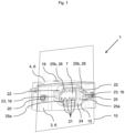
- Fig. 1 shows a perspective view of the sensor unit 1, wherein the sensor unit 1 has a first housing part 3 and a second housing part 4, wherein the two housing parts 3, 4 are connected to one another in a force-fitting manner by means of two screws 20.
- the first and the second housing part 3, 4 each have a housing part outer side 6, wherein the housing part outer side 6 of the first housing part 3 is designed such that a contact area 7 is arranged thereon, which is bordered by a formation 15 of the first housing part 3.
- the formation 15 has a length extending orthogonally away from a main plane 10, which is longer than the length of contact points 21 of the contact area 7 in order to protect them from impacts and other external influences.
- the formation 15 has a Formation opening 23, which forms a connection option 16 for the mechanical connection of the sensor unit 1 to a machine unit (not shown).
- the formation openings 23 can be penetrated in particular by means of a snap hook (not shown) arranged on the machine side in order to form a detachable, positive-locking connection between the sensor unit 1 and the machine unit.
- the connection option 16 is further offset from an inner formation surface 24 of the formation 15 in such a way that a formation guide 25a is formed for attaching the sensor unit 1 to the machine unit.
- the formation 15 has two formation grooves 26 on its inner formation surface 24, said grooves having a different width.
- the formation grooves 26 are designed as further formation guides 25b and to prevent improper attachment of the sensor unit 1 to the machine unit.
- the second housing part 4 has on its housing part outer side 6 a light guide 19 which is positively connected to the second housing part 4, wherein the light guide 19 is overmolded by the second housing part 4.
- Fig. 2 shows a perspective exploded view of the sensor unit 1, wherein in an interior space 5 (not shown) between the first and second housing parts 3, 4, an electronics unit 2 with a first and a second circuit board section 9a, 9b is arranged, wherein the circuit board sections 9a, 9b are each designed as individual circuit boards 8a, 8b according to the invention.
- the first circuit board 8a is arranged orthogonally to the second circuit board 8b, wherein the first circuit board 8a is arranged parallel to the main plane 10 and contacts the contact area 7, wherein the contact area 7 is plugged onto the first circuit board 8a by means of contact points 21 and is soldered mechanically onto the first circuit board 8a.
- a first transmission unit 27a is also arranged according to the invention on the first circuit board 8a, wherein the first transmission unit 27a receives a second transmission unit 27b arranged on the second circuit board 8b and thus forms the electrically conductive connection between the first and second circuit boards 8a, 8b.
- a support structure 11 is formed between the first and second circuit boards 8a, 8b and is connected to the first and second circuit boards 8a, 8b via a screw connection using two screws 20 each. The two screws 20 for connecting the support structure 11 to the first circuit board 8a are screwed into the first housing part 3 and the first circuit board 8a is thereby clamped between the latter and the support structure 11.
- the first housing part 3 has lugs 28 which are received in support structure grooves 29 in order to ensure reliable positioning of the first circuit board 8a and the support structure 11 on the first housing part 3.
- the support structure 11 has a frame/truss construction to absorb any stresses or forces that occur and to transmit them as directly as possible to the circuit boards 8a, 8b.
- the support structure 11 has guide webs 30 that are guided in a non-visible guide 12 of the second housing part 4, wherein the guide 12 is designed as a groove.
- the width of the guide web 30 increases in the direction of the main plane 10.
- the non-visible guide 12 is tapered in width away from the main plane 10, so that a force-fitting connection, in particular a clamping connection, is formed between the second housing part 4 and the support structure 11.
- a reliable hold between the second housing part 4 and the support structure 11 and thus also the electronics unit 2 and the second housing part 4 is thus ensured.
- a molded seal 13 is formed between the first and second housing parts 3, 4. Furthermore, the shaped seal 13 has a shaped sealing nose 40, which is located in a shaped sealing recess 41 of the second housing part 4 can be received. This arrangement advantageously makes it possible to detect, even in the installed state, whether the molded seal 13 is arranged between the first and second housing parts 3, 4.
- the second housing part 4 On a housing part outer side 6 of the second housing part 4, which is formed opposite the housing part outer side 6 on which the invisible light guide 19 is arranged, the second housing part 4 has a pressure equalization opening 31, which is surrounded on one side by a pressure equalization membrane 32 in the operating state.
- the second housing part 4 also has two offset sections 33, wherein section openings 34 are formed on the offset sections 33, the axes of which are arranged parallel to the main plane 10 and which in turn have section webs 35 running parallel to the main plane 10 for each receiving a sleeve 36.
- the sleeves 36 can be clamped within the section openings 34 by means of the section webs 35 and are designed to accommodate a screw and the associated clamping force. Accordingly, the second housing part 4, which is made of a plastic, is protected from damage or even destruction by resulting clamping forces.
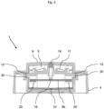
- Fig. 3 shows a section of the sensor unit 1 in a side view, wherein the guide webs 30 of the support structure 11 are accommodated within the guides 12 of the second housing part 4.
- the guide 12 is designed as a tapered groove extending into the image plane.
- the light guide 19 is designed such that it projects from the housing part outer side 6 into the interior 5, wherein the distance between the light guide 19 and a light source 18 arranged on the second circuit board 8b is as small as possible in order to prevent unwanted scattering of the light from the light source 18 as well as damage to the circuit boards 8a, 8b and the light source 18 during disassembly and assembly.
- the light source 18 is designed as an LED, which States red and green, where red represents a fault and green represents fault-free functionality of the sensor unit 1.
- the second circuit board 8b is fixedly mounted on the support structure 11 by means of screws 20.
- a pressure equalization opening 31 is arranged on the second housing part 4 opposite the light guide 19.
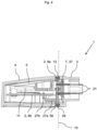
- Fig. 4 shows a further section of the sensor unit 1 in a different side view, wherein the first housing part 3 is penetrated by the contact area 7, which has contact points 21 in the form of pins that penetrate the first circuit board 8a, as well as a contact frame 37.
- the contact frame 37 is arranged between the contact points 21 and the first housing part 3, rests positively on the first housing part 3 and is pressed together with the contact points 21.
- the contact frame 37 is advantageously made of a material comparable to the first housing part 3 in order to transmit external stresses, forces or vibrations acting on the first housing part 3 directly to the electronics unit 2.
- the molded seal 13 rests positively on the second housing part 4 around the first circuit board 8a, wherein the second housing part 4 has a molded seal web 39 corresponding to a molded seal groove 38 of the molded seal 13 for the form fit.
- Contact between the first and second circuit boards 8a, 8b is prevented by the support structure 11, so that the first and second circuit boards 8a, 8b are only electrically connected to one another via the first and second transmission units 27a, 27b.
- the first and second circuit boards 8a and 8b are located to the left of the main plane 10, which is defined by a contact surface between the first and second housing parts 3, 4.
- the first and second housing parts 3, 4 are designed on their contact surface in such a way that, adjacent to the contact surface, they accommodate the molded seal 13 between them in such a way that over-pressing and thus damage or even destruction of the molded seal 13 is prevented, and functional pressing of the However, a molded seal 13 is possible to ensure reliable sealing of the interior space 5.
- the first housing part 3 does not cover the part of the electronics unit 2 that projects into the interior space 5.
Landscapes
- Physics & Mathematics (AREA)
- General Physics & Mathematics (AREA)
- Engineering & Computer Science (AREA)
- Radar, Positioning & Navigation (AREA)
- Remote Sensing (AREA)
- Casings For Electric Apparatus (AREA)
Description
- Die vorliegende Erfindung betrifft eine Sensoreinheit aufweisend eine Elektronikeinheit, einen ersten Gehäuseteil und einen damit verbundenen zweiten Gehäuseteil, wobei die Elektronikeinheit mit dem ersten Gehäuseteil verbunden und in den Innenraum ragend ist, wobei ein den ersten Gehäuseteil durchsetzender Kontaktbereich vorgesehen ist, wobei die Elektronikeinheit mindestens eine Leiterplatte mit mindestens zwei, miteinander elektrisch leitend verbundenen, Leiterplattenabschnitten aufweist.
- Sensoreinheiten, insbesondere Lage- oder Neigungssensoren, werden unter anderem in rauen, von starken Umwelteinflüssen bestimmten Umgebungen eingesetzt. Zudem werden diese an verschiedenste Maschineneinheiten, wie Fahrzeuge oder Produktionsmaschinen angebracht und müssen daher entsprechend verschiedenartig ausgebildet sein.
- Aus dem Stand der Technik sind Sensoreinheiten bekannt, die an bzw. in einem Gehäuse einen Kontaktbereich zur elektrischen Verbindung mit der jeweiligen Maschineneinheit sowie eine Leiterplatte aufweisen, wobei Leiterplatte und Kontaktbereich üblicherweise mittels isolierter Leitungen innerhalb des Gehäuses der Sensoreinheit miteinander verbunden sind. Um sowohl die Leiterplatte als auch die Leitungen und den Kontaktbereich innerhalb des Gehäuses vor äußeren Einflüssen zu schützen, wird das restliche Volumen des Gehäuses üblicherweise beispielsweise mit einem Silikon oder Harz ausgegossen. Dies schützt diese Bauteile sicher, erschwert jedoch nachträglich Änderungen oder Modulationen der Hardware der Sensoreinheit. Die Leiterplatte ist nicht länger zerstörungsfrei erreichbar oder recyclebar.
- Die
US 4,864,156 offenbart einen Näherungsschalter, der ein Hauptgehäuse, ein Zwischensteckergehäuse und ein Sensorgehäuse aufweist, wobei jeweils eine Leiterplatte in einem Gehäuse angeordnet ist und die Leiterplatten des Zwischensteckergehäuses und des Sensorgehäuses elektrisch leitend miteinander verbunden sind und die Leiterplatten des Zwischensteckergehäuses und des Hauptgehäuses galvanisch voneinander getrennt sind. - Die
US 2003/0123242 A1 offenbart ein Gehäuse für einen Sensor, wobei das Sensorgehäuse an mindestens einer Gehäuseseite eine Beschichtung aufweist, welche besonders resistent gegenüber äußeren Einflüssen wie Schweißblitzen ist. Darüber hinaus weist das Gehäuse drei Gehäuseteile auf, die einen Innenraum definieren, in dem eine Elektronikeinheit angeordnet ist. - Die
US 2010/097050 A1 offenbart einen Abstandssensor. - Die vorliegende Erfindung stellt sich daher die Aufgabe, eine möglichst einfach zu montierende, robuste und leicht transformierbare Sensoreinheit anzugeben.
- Diese Aufgabe wird gelöst durch eine Sensoreinheit aufweisend eine Elektronikeinheit, einen ersten Gehäuseteil und einen damit verbundenen zweiten Gehäuseteil, wobei erster und zweiter Gehäuseteil zwischen sich einen Innenraum bilden und von diesem jeweils weggerichtet je eine Gehäuseteilaußenseite aufweisen, wobei die Elektronikeinheit mit dem ersten Gehäuseteil verbunden und in den Innenraum ragend ist, wobei ein den ersten Gehäuseteil durchsetzender Kontaktbereich vorgesehen ist, wobei die Elektronikeinheit mindestens eine Leiterplatte mit mindestens zwei, miteinander elektrisch leitend verbundenen, Leiterplattenabschnitten aufweist, wobei ein erster Leiterplattenabschnitt elektrisch leitend zwischen dem Kontaktbereich und einem zweiten Leiterplattenabschnitt angeordnet ist.
- Erster und zweiter Gehäuseteil sind vorteilhaft kraftschlüssig oder formschlüssig reversibel miteinander verbunden, um bei einer möglichen Anpassung der Elektronikeinheit den Innenraum für einen Nutzer ohne Weiteres zugänglich zu machen. Sie sind bevorzugt aus einem Kunststoff mit hoher Festigkeit, Steifigkeit, und sehr guten Reibwiderständen gebildet, vorteilhaft aus ABS oder PBT, insbesondere mit Glasfaser verstärkt. Der Innenraum ist erfindungsgemäß derart ausgebildet, dass er neben sämtlichen im Innenraum angeordneten Komponenten auch ein Gas aufnimmt, insbesondere Umgebungsluft oder Stickstoff, was mögliche Temperaturschwankungen durch äußere Einflüsse, welche gegebenenfalls die Messergebnisse beeinflussen, verhindert. Die Nutzung eines Gases wie Stickstoff zum Befüllen des Innenraumes verhindert erfindungsgemäß ein Entflammen des Innenraums bei einer Fehlfunktion der Sensoreinheit. Die Elektronikeinheit ist mindestens mittelbar mit dem ersten Gehäuseteil verbunden, insbesondere kraft- und/oder formschlüssig. Der Kontaktbereich weist mindestens einen Kontaktpunkt sowie einen Kontaktrahmen auf, wobei der Kontaktrahmen einstückig mit dem ersten Gehäuseteil oder alternativ kraft- oder formschlüssig mit diesem verbunden ist. Erfindungsgemäß sind Elektronikkomponenten abhängig von ihrer Verwendung auf dem ersten oder dem zweiten Leiterplattenabschnitt angeordnet. Der erste und der zweite Leiterplattenabschnitt können erfindungsgemäß einstückig oder als zwei einzelne, sogar örtlich voneinander getrennten Leiterplatten ausgebildet sein. Der Vorteil einer Nutzung von zwei einzelnen und unabhängig voneinander angeordneten Leiterplattenabschnitten ist deren flexible Kombinationsmöglichkeit miteinander. Demnach sind vorteilhaft alle Elektronikkomponenten einer Aufgabenstellung auf einem Leiterplattenabschnitt und die einer anderen Aufgabenstellung auf einem anderen Leiterplattenabschnitt angeordnet. Es ergibt sich so ein Baukastenprinzip, wonach die Sensoreinheit je nach Anwendungsfall optimal an die jeweiligen Anforderungen angepasst werden kann. Dies ermöglicht eine hohe Modularität und Einsetzbarkeit in verschiedensten Verwendungsbereichen unter einer nur geringfügigen Änderung eines Teilbereichs der Elektronikeinheit. Die elektrisch leitende Anordnung des ersten Leiterplattenabschnittes zwischen dem Kontaktbereich und dem zweiten Leiterplattenabschnitt trägt maßgeblich zu den zuvor genannten Vorteilen der Erfindung bei, da hierdurch eine normierte Verbindung zwischen erstem und zweiten Leiterplattenabschnitt ausgebildet ist und die Leiterplattenabschnitte unabhängig von den darauf angeordneten Elektronikkomponenten oder einem angeordneten Kontaktbereich miteinander verbindbar und einsetzbar sind.
- In Ausgestaltung der Erfindung ist vorgesehen, dass der erste Leiterplattenabschnitt im Betriebszustand an dem Kontaktbereich anliegende elektrische Spannung und/oder Stromstärke an den zweiten Leiterplattenabschnitt im Wesentlichen unverändert übertragend ist. In besonders vorteilhafter Weise sind die Elektronikkomponenten, die zur Kontaktierung des Kontaktbereiches und damit zur Verbindung mit der restlichen Maschine ausgebildet sind, auf dem ersten Leiterplattenabschnitt angeordnet, um bei Veränderung des Kontaktbereichs gegebenenfalls lediglich den ersten Leiterplattenabschnitt anpassen zu müssen. Eine Anordnung weiterer Elektronikkomponenten auf dem ersten Leiterplattenabschnitt, insbesondere von Leuchtmitteln oder optischen Anzeigen, welche unabhängig von den, auf dem zweiten Leiterplattenabschnitt angeordneten, Elektronikkomponenten funktionsfähig sind, ist ebenfalls vorteilhaft. Zudem sind in besonders vorteilhafter Weise Elektronikkomponenten wie Sicherungen, insbesondere Feinsicherungen oder 0 Ω Widerstände auf dem ersten Leiterplattenabschnitt zur flexiblen elektrischen Kontaktierung zwischen dem mindestens einen Kontaktpunkt und verschiedenen Bereichen des ersten Leiterplattenabschnittes angeordnet. Die für die eigentliche Funktion der Sensoreinheit notwendigen Elektronikkomponenten müssen nicht umgeordnet werden, da die elektromagnetischen Störfelder des sich ändernden ersten Leiterplattenabschnitts durch die abgegrenzte Anordnung lediglich einen sehr geringen oder keinen Einfluss haben. Ebenso besteht die Möglichkeit, den ersten Leiterplattenabschnitt mit einem für eine Maschineneinheit passenden Kontaktbereich an einen funktional anderen zweiten Leiterplattenabschnitt anzuordnen, um mehrere verschieden wirkende Sensoreinheiten für einen Steckplatz zu erhalten. Mit anderen Worten ist der Vorteil zweifach: zum einen kann ein Hersteller der erfindungsgemäßen Sensoren einen bereits für eine Maschine ausgebildeten Sensor sehr einfach anpassen, sollte sich maschinenseitig eine Änderung ergeben, zum anderen kann der Hersteller unterschiedliche Sensoren in ein und demselben Gehäuse mit ein und demselben Kontaktbereich anordnen und so dem Maschinenhersteller unterschiedliche Sensoren zur Auswahl stellen, ohne dass der Maschinenhersteller unterschiedliche Kontaktmöglichkeiten bereitstellen müsste.
- In vorteilhafter Weise ist der erste Gehäuseteil derart im Wesentlichen plattenförmig ausgebildet, dass er einen geringeren Teil des in den Innenraum des Gehäuses ragenden Teils der Elektronikeinheit überdeckt als der zweite Gehäuseteil. Aufgrund des im Wesentlichen plattenförmigen ersten Gehäuseteils sind sämtliche Komponenten während der Montage der Elektronikeinheit frei zugänglich, ein Hineingreifen in einen engen Innenraum ist nicht erforderlich. Hierbei ist die plattenförmige Ausbildung des ersten Gehäuseteils in erster Linie so zu verstehen, dass der erste Gehäuseteil seine maximale Querschnittsfläche parallel zu seiner Hauptebene aufweist.
- In Weiterbildung der Erfindung ist vorgesehen, dass der erste Gehäuseteil weniger als 30%, insbesondere weniger als 20%, vorzugsweise weniger als 10% des in den Innenraum ragenden Teils der Elektronikeinheit überdeckt. In besonders vorteilhafter Weise sind demnach sämtliche Einheiten, welche im Innenraum angeordnet sind, an dem ersten Gehäuseteil montierbar und zudem leicht zugänglich. Der zweite Gehäuseteil schließt den Innenraum ab, sodass die Elektronikeinheit darin sicher aufgenommen ist.
- In Ausgestaltung der Erfindung ist vorgesehen, dass ein Leiterplattenabschnitt der Elektronikeinheit im Wesentlichen parallel zu der Hauptebene des plattenförmigen ersten Gehäuseteils orientiert und die Elektronikeinheit mit diesem mindestens mittelbar an dem ersten Gehäuseteil befestigt ist und/oder die zwei Leiterplattenabschnitte im Wesentlichen orthogonal zueinander angeordnet sind. In besonders vorteilhafter Weise ist der Kontaktrahmen des Kontaktbereichs parallel und je nach Beschaffenheit der Kontaktpunkte dicht zu dem parallel zur Hauptebene angeordneten Leiterplattenabschnitt angeordnet sowie der mindestens eine Kontaktpunkt im Wesentlichen orthogonal zu dem Kontaktrahmen und zu dem parallel zur Hauptebene angeordneten Leiterplattenabschnitt angeordnet ist. Übertragungsleitungen, welche einen zusätzlichen Aufnahmeraum benötigen würden und zudem anfällig für Beschädigungen durch Stöße oder Vibrationen sind, sind vorteilhaft vermieden. Je weniger elektrische Kontaktierungsstellen notwendig sind, umso geringer ist das Risiko einer Beschädigung, Zerstörung oder fehlerhaften Fertigung einer von diesen. Die feste Verbindung zwischen dem parallel zur Hauptebene angeordneten Leiterplattenabschnitt und dem Kontaktbereich durch das direkte Auflöten des mindestens einen Kontaktpunktes auf den parallel zur Hauptebene angeordneten Leiterplattenabschnitts ermöglicht durch eine form- und/oder kraftschlüssige Verbindung zwischen dem Kontaktbereich und dem ersten Gehäuseteil eine zuverlässige Positionierung der Elektronikeinheit, was eine Beschädigung dieser und des Kontaktbereichs minimiert. Der mindestens eine Kontaktpunkt ist dabei form- und/oder kraftschlüssig mit dem Kontaktrahmen verbunden, wobei der mindestens eine Kontaktpunkt insbesondere mit dem Kontaktrahmen verpresst ist. Die Ausbildung des Kontaktrahmen als getrennte Komponente zu dem ersten Gehäuseteil ist vorteilhaft, da durch dessen flache zum ersten Leiterplattenabschnitt parallel ausgerichtete Hauptfläche der mindestens eine Kontaktpunkt auf den ersten Leiterplattenabschnitt in einer durch den Kontaktrahmen vordefinierten Anordnung maschinell auflötbar, insbesondere mittels Wellenlöten verbindbar ist. Bei einer einstückigen Ausbildung des Kontaktrahmens mit dem ersten Gehäuseteil ist die erforderliche Maßeinhaltung zur korrekten Positionierung des mindestens einen Kontaktpunktes auf Grund der geringeren Anzahl an Toleranzbereichen vereinfacht. Eine zuverlässige Positionierung der Elektronikeinheit ist bei dieser Ausführungsform über eine formschlüssige Verbindung zwischen Elektronikeinheit und erstem Gehäuseteil ausbildbar. Die orthogonale Anordnung der zwei Leitplattenabschnitte ist besonders vorteilhaft, da hierdurch eine platzsparende und modulartige Elektronikeinheit ausgebildet ist.
- Erfindungsgemäß weist die Sensoreinheit eine am ersten Gehäuseteil befestigte und die Elektronikeinheit kontaktierende Stützkonstruktion auf, wobei die Stützkonstruktion in einer Führung des zweiten Gehäuseteils geführt ausgebildet ist. Die Stützkonstruktion ist bevorzugt lösbar mit dem ersten Gehäuseteil und/oder der Elektronikeinheit verbunden. Insbesondere ist die Verbindung als eine kraft- oder formschlüssige, besonders bevorzugt als eine Schraubverbindung ausgebildet. Die Stützkonstruktion ist derart ausgebildet, dass zwischen ihr und der Elektronikeinheit eine möglichst starre Verbindung zur direkten Übertragung von auftretenden Kräften oder Vibrationen ausgebildet ist. Damit trägt die Elektronikeinheit neben der Stützkonstruktion zur Steigerung der Gesamtfestigkeit der Sensoreinheit bei.
- In einer Weiterbildung der Erfindung ist zwischen erstem und zweitem Gehäuseteil eine Formdichtung angeordnet. Die Formdichtung dichtet vorteilhaft den Innenraum vor Schmutz, Wasser und Staub ab, insbesondere weist der Innenraum auch hierdurch mindestens die Schutzklasse IP 68 auf. Die Formdichtung ist vorteilhaft aus einem Gummi, insbesondere aus EPDM, NBR, FKM oder BR ausgebildet.
- In Ausgestaltung der Erfindung ist vorgesehen, dass der Kontaktbereich von einer Ausformung des ersten Gehäuseteils umrandet umgeben ausgebildet ist. Die Ausformung schützt vorteilhaft den Kontaktbereich vor einer Beschädigung. Sofern der Kontaktbereich als einer mit vielen von der Hauptebene wegragenden Kontaktpunkten ausgebildet ist, weist die Ausformung mindestens die Länge der wegragenden Kontaktpunkte auf, um diese vor einer Beschädigung zu schützen. Die Ausformung weist vorteilhaft Ausformungsnuten auf. Eine Ausbildung der Ausformungsnuten als Ausformungsstege ist ebenfalls vorteilhaft, um ein sicheres Einführen des Kontaktbereichs in eine Maschineneinheit zu gewährleisten und im Kontaktbereich auftretende Querkräfte, welche zu einer Beschädigung führen könnten, möglichst zu minimieren. Bevorzugt ist die Ausformung derart ausgebildet, dass sie eine fehlerhafte Kontaktierung zwischen Kontaktbereich und einer Maschineneinheit, insbesondere über unterschiedlich ausgestaltete Ausformungsführungen oder Ausformungsnuten verhindernd ist.
- In vorteilhafter Weise weist der erste Gehäuseteil mindestens eine Verbindungsmöglichkeit zur mechanischen Verbindung der Sensoreinheit mit einer Maschineneinheit auf. Die Nutzung einer handelsüblichen Verbindungsmöglichkeit ist hierbei vorteilhaft. In besonders vorteilhafter Weise ist die Verbindungsmöglichkeit reversibel, insbesondere als Schnapphaken, Bajonett, oder Schraubverbindung ausgebildet. Demnach ist die Verbindung zwischen Sensoreinheit und Maschineneinheit kraftschlüssig und/oder formschlüssig. Die Verbindungsmöglichkeit ist vorteilhaft möglichst nahe, bzw. neben dem Kontaktbereich, insbesondere innerhalb der Ausformung des ersten Gehäuseteils, welche den Kontaktbereich umrandet, ausgebildet. Somit ist eine zuverlässige Kontaktierung des Kontaktbereiches auch bei aufkommenden Vibrationen oder Stößen durch die Maschineneinheit oder andere Umgebungseinflüsse gewährleistet.
- In Weiterbildung der Erfindung ist vorgesehen, dass der zweite Gehäuseteil eine optische Anzeige aufweist, insbesondere eine durch ein auf der Leiterplatte angeordnetes Leuchtmittel und einem in dem zweiten Gehäuseteil endenden Lichtleiter und/oder ein durch einen lichtdurchlässigen Abschnitt im zweiten Gehäuseteil gebildetes Leuchtmittel. Die optische Anzeige ermöglicht die Erkennung von beispielsweise einer korrekten Kontaktierung zwischen Maschineneinheit und Kontaktbereich für einen Anwender. Ebenfalls können durch die optische Anzeige vorteilhaft Warnsignale beispielsweise bei Überhitzung oder falscher Kontaktierung ausgegeben werden. Die Ausgabe eines Messwertes direkt an der Sensoreinheit über die optische Anzeige ist ebenfalls möglich. Das Leuchtmittel ist in vorteilhafter Weise als mindestens eine LED ausgebildet, wobei auch ein LCD oder eine Segmentanzeige einsetzbar ist. Der Lichtleiter oder der lichtdurchlässige Abschnitt sind vorteilhaft formschlüssig, kraftschlüssig oder stoffschlüssig mit dem zweiten Gehäuseteil verbunden, wobei der Lichtleiter im Wesentlichen dieselben mechanischen Eigenschaften, insbesondere ähnliche Festigkeiten und ähnliche Wärmeausdehnungskoeffizienten wie der zweite Gehäuseteil aufweist und demnach keine Schwachstelle in Bezug auf die Stabilität des zweiten Gehäuseteils darstellt. In besonders vorteilhafter Weise ist der Lichtleiter oder der lichtdurchlässige Abschnitt von dem zweiten Gehäuseteil umspritzt, was zum einen eine formschlüssige bzw. stoffschlüssige unlösbare und zum anderen eine dichtende Verbindung ausbildet. Ebenfalls kann der lichtdurchlässige Abschnitt als eine Durchgangsöffnung ausgebildet sein, wobei das Leuchtmittel selbst formschlüssig oder kraftschlüssig und dichtend mit dem zweiten Gehäuseteil verbunden ist.
- Die Erfindung wird nachfolgend anhand eines Ausführungsbeispiels mittels der Figuren näher erläutert, wobei
- Fig. 1
- eine perspektivische Ansicht der Sensoreinheit,
- Fig. 2
- eine perspektivische Explosionsansicht der Sensoreinheit,
- Fig. 3
- einen Schnitt der Sensoreinheit in einer Seitenansicht und
- Fig. 4
- einen weiteren Schnitt der Sensoreinheit in einer anderen Seitenansicht zeigen.
-
Fig. 1 zeigt eine perspektivische Ansicht der Sensoreinheit 1, wobei die Sensoreinheit 1 einen ersten Gehäuseteil 3 und einen zweiten Gehäuseteil 4 aufweist, wobei die beiden Gehäuseteile 3, 4 mittels zwei Schrauben 20 kraftschlüssig miteinander verbunden sind. Der erste und der zweite Gehäuseteil 3, 4 weisen jeweils eine Gehäuseteilaußenseite 6 auf, wobei die Gehäuseteilaußenseite 6 des ersten Gehäuseteils 3 derart ausgebildet ist, dass an diesem ein Kontaktbereich 7 angeordnet ist, welcher von einer Ausformung 15 des ersten Gehäuseteils 3 umrandet ist. Die Ausformung 15 weist eine sich von einer Hauptebene 10 orthogonal weg erstreckende Länge auf, die länger als die Länge von Kontaktpunkten 21 des Kontaktbereichs 7 ist, um diese vor Stößen und anderen äußeren Einflüssen zu schützen. Weiter weist die Ausformung 15 an zwei sich gegenüberliegenden Ausformungswänden 22 jeweils eine Ausformungsöffnung 23 auf, was eine Verbindungsmöglichkeit 16 zur mechanischen Verbindung der Sensoreinheit 1 mit einer nicht dargestellten Maschineneinheit ausbildet. Die Ausformungsöffnungen 23 sind insbesondere mittels eines maschinenseitig angeordneten nicht dargestellten Schnapphakens durchsetzbar, um eine lösbare formschlüssige Verbindung zwischen Sensoreinheit 1 und Maschineneinheit auszubilden. Die Verbindungsmöglichkeit 16 ist weiter derart versetzt zu einer Ausformungsinnenfläche 24 der Ausformung 15 ausgebildet, dass eine Ausformungsführung 25a zum Anbringen der Sensoreinheit 1 an die Maschineneinheit ausgebildet ist. Darüber hinaus weist die Ausformung 15 an deren Ausformungsinnenfläche 24 zwei Ausformungsnuten 26 auf, wobei diese eine unterschiedliche Breite aufweisen. Die Ausformungsnuten 26 sind als weitere Ausformungsführungen 25b und zur Verhinderung eines unsachgemäßen Aufsteckens der Sensoreinheit 1 auf die Maschineneinheit ausgebildet. Der zweite Gehäuseteil 4 weist an seiner Gehäuseteilaußenseite 6 einen Lichtleiter 19 auf, der formschlüssig mit dem zweiten Gehäuseteil 4 verbunden ist, wobei der Lichtleiter 19 von dem zweiten Gehäuseteil 4 umspritzt ist. -
Fig. 2 zeigt eine perspektivische Explosionsansicht der Sensoreinheit 1, wobei in einem nicht dargestellten Innenraum 5 zwischen erstem und zweitem Gehäuseteil 3, 4 eine Elektronikeinheit 2 mit einem ersten und einem zweiten Leiterplattenabschnitt 9a, 9b angeordnet ist, wobei die Leiterplattenabschnitte 9a, 9b erfindungsgemäß jeweils als einzelne Leiterplatten 8a, 8b ausgebildet sind. Die erste Leiterplatte 8a ist orthogonal zu der zweiten Leiterplatte 8b angeordnet, wobei die erste Leiterplatte 8a parallel zur Hauptebene 10 angeordnet ist und den Kontaktbereich 7 kontaktiert, wobei der Kontaktbereich 7 auf die erste Leiterplatte 8a mittels Kontaktpunkten 21 aufgesteckt und maschinell auf der ersten Leiterplatte 8a aufgelötet ist. Eine erste Übertragungseinheit 27a ist erfindungsgemäß ebenfalls auf der ersten Leiterplatte 8a angeordnet, wobei die erste Übertragungseinheit 27a eine, auf der zweiten Leiterplatte 8b angeordnete, zweite Übertragungseinheit 27b aufnimmt und damit die elektrisch leitende Verbindung zwischen erster und zweiter Leiterplatte 8a, 8b ausbildet. Zwischen erster und zweiter Leiterplatte 8a, 8b ist eine Stützkonstruktion 11 ausgebildet, die über eine Schraubverbindung durch jeweils zwei Schrauben 20 mit der ersten und zweiten Leiterplatte 8a, 8b verbunden ist. Die zwei Schrauben 20 zur Verbindung der Stützkonstruktion 11 mit der ersten Leiterplatte 8a werden in den ersten Gehäuseteil 3 eingeschraubt und die erste Leiterplatte 8a dadurch zwischen diesem und der Stützkonstruktion 11 verklemmt. Der erste Gehäuseteil 3 weist Nasen 28 auf, die in Stützkonstruktionsnuten 29 aufgenommen werden, um eine zuverlässige Positionierung der ersten Leiterplatte 8a und der Stützkonstruktion 11 an dem ersten Gehäuseteil 3 zu gewährleisten. Die Stützkonstruktion 11 weist eine Rahmen-/ Fachwerkkonstruktion auf, um auftretende Spannungen oder Kräfte aufzunehmen und diese möglichst direkt an die Leiterplatten 8a, 8b zu übertragen. Erfindungsgemäß weist die Stützkonstruktion 11 Führungsstege 30 auf, die in einer nicht sichtbaren Führung 12 des zweiten Gehäuseteils 4 geführt werden, wobei die Führung 12 als Nut ausgebildet ist. Die Breite des Führungssteges 30 nimmt in Richtung der Hauptebene 10 zu. Die nicht sichtbare Führung 12 ist in ihrer Breite von der Hauptebene 10 wegweisend verjüngt ausgebildet, sodass zwischen zweitem Gehäuseteil 4 und der Stützkonstruktion 11 eine kraftschlüssige Verbindung, insbesondere eine Verklemmung ausgebildet ist. Ein zuverlässiger Halt zwischen zweitem Gehäuseteil 4 und Stützkonstruktion 11 und damit auch Elektronikeinheit 2 und zweitem Gehäuseteil 4 ist demnach sichergestellt. Zwischen erstem und zweitem Gehäuseteil 3, 4 ist eine Formdichtung 13 ausgebildet. Weiter weist die Formdichtung 13 eine Formdichtungsnase 40 auf, welche in einer Formdichtungsaussparung 41 des zweiten Gehäuseteils 4 aufnehmbar ist. Durch diese Anordnung kann mit Vorteil auch im eingebauten Zustand erkannt werden, ob die Formdichtung 13 zwischen dem ersten und zweiten Gehäuseteil 3, 4 angeordnet ist. An einer Gehäuseteilaußenseite 6 des zweiten Gehäuseteils 4, welche gegenüber der Gehäuseteilaußenseite 6 ausgebildet ist, an der der nicht sichtbare Lichtleiter 19 angeordnet ist, weist der zweite Gehäuseteil 4 eine Druckausgleichsöffnung 31 auf, die einseitig von einer Druckausgleichsmembran 32 im Betriebszustand umgeben ist. Der zweite Gehäuseteil 4 weist darüber hinaus zwei abgesetzte Abschnitte 33 auf, wobei an den abgesetzten Abschnitten 33 Abschnittsöffnungen 34 ausgebildet sind, deren Achsen parallel zur Hauptebene 10 angeordnet sind und die wiederum parallel zur Hauptebene 10 verlaufende Abschnittsstege 35 zur Aufnahme jeweils einer Hülse 36 aufweisen. Die Hülsen 36 sind mittels der Abschnittsstege 35 innerhalb der Abschnittsöffnungen 34 verklemmbar anordenbar und zur Aufnahme einer Schraube und der damit verbundenen Klemmkraft ausgebildet. Demnach ist der zweite Gehäuseteil 4, welcher aus einem Kunststoff gefertigt ist, vor Beschädigung oder gar Zerstörung durch aufkommende Klemmkräfte geschützt. -
Fig. 3 zeigt einen Schnitt der Sensoreinheit 1 in einer Seitenansicht, wobei die Führungsstege 30 der Stützkonstruktion 11 innerhalb der Führungen 12 des zweiten Gehäuseteils 4 aufgenommen sind. Die Führung 12 ist in die Bildebene hineinreichend als eine sich verjüngende Nut ausgebildet. Der Leichtleiter 19 ist derart ausgebildet, dass er von der Gehäuseteilaußenseite 6 in den Innenraum 5 hineinragt, wobei der Abstand zwischen Lichtleiter 19 und einem auf der zweiten Leiterplatte 8b angeordneten Leuchtmittel 18 möglichst gering ist, um eine ungewollte Streuung des Lichtes des Leuchtmittels 18 sowie eine Beschädigung der Leiterplatten 8a, 8b und des Leuchtmittels 18 bei De- und Montage zu verhindern. Das Leuchtmittel 18 ist als eine LED ausgebildet, welche die Zustände rot und grün aufweist, wobei rot für eine Störung und grün für eine störungsfreie Funktionalität der Sensoreinheit 1 steht. Die zweite Leiterplatte 8b ist mittels Schrauben 20 an der Stützkonstruktion 11 fest angeordnet. Gegenüberliegend von dem Lichtleiter 19 ist eine Druckausgleichsöffnung 31 an dem zweiten Gehäuseteil 4 angeordnet. -
Fig. 4 zeigt einen weiteren Schnitt der Sensoreinheit 1 in einer anderen Seitenansicht, wobei der erste Gehäuseteil 3 durch den Kontaktbereich 7 durchsetzt ist, welcher Kontaktpunkte 21 in Form von Pins, die die erste Leiterplatte 8a durchsetzen, sowie einen Kontaktrahmen 37 aufweist. Der Kontaktrahmen 37 ist zwischen den Kontaktpunkten 21 und dem ersten Gehäuseteil 3 angeordnet, liegt formschlüssig an dem ersten Gehäuseteil 3 an und ist mit den Kontaktpunkten 21 verpresst. Der Kontaktrahmen 37 ist in vorteilhafterweise aus einem zum ersten Gehäuseteil 3 vergleichbaren Material ausgebildet, um eine Übertragung von äußeren auf den ersten Gehäuseteil 3 einwirkenden Spannungen, Kräften oder Vibrationen direkt auf die Elektronikeinheit 2 zu übertragen. Um die erste Leiterplatte 8a liegt die Formdichtung 13 an dem zweiten Gehäuseteil 4 formschlüssig an, wobei der zweite Gehäuseteil 4 zum Formschluss einen einer Formdichtungsnut 38 der Formdichtung 13 entsprechenden Formdichtungssteg 39 aufweist. Eine Berührung der ersten und zweiten Leiterplatte 8a, 8b ist durch die Stützkonstruktion 11 verhindert, sodass die erste und zweite Leiterplatte 8a, 8b lediglich über die erste und zweite Übertragungseinheit 27a, 27b miteinander elektrisch leitend verbunden sind. Die erste und zweite Leiterplatte 8a und 8b befinden sich links von der Hauptebene 10, welche durch eine Anlagefläche zwischen erstem und zweiten Gehäuseteil 3, 4 definiert ist. Erster und zweiter Gehäuseteil 3, 4 sind derart an ihrer Anlagefläche ausgebildet, dass sie benachbart zur Anlagefläche die Formdichtung 13 zwischen sich derart aufnehmend sind, dass ein Überpressen und damit eine Beschädigung oder gar Zerstörung der Formdichtung 13 verhindert ist, ein funktionales Anpressen der Formdichtung 13 zur Ausbildung einer zuverlässigen Dichtheit des Innenraums 5 allerdings möglich ist. Der erste Gehäuseteil 3 ist den in den Innenraum 5 ragenden Teil der Elektronikeinheit 2 nicht überdeckend. -
- 1
- Sensoreinheit
- 2
- Elektronikeinheit
- 3
- Erster Gehäuseteil
- 4
- Zweiter Gehäuseteil
- 5
- Innenraum
- 6
- Gehäuseteilaußenseite
- 7
- Kontaktbereich
- 8, 8a, 8b
- Leiterplatte
- 9, 9a, 9b
- Leiterplattenabschnitt
- 10
- Hauptebene
- 11
- Stützkonstruktion
- 12
- Führung
- 13
- Formdichtung
- 15
- Ausformung
- 16
- Verbindungsmöglichkeit
- 17
- Optische Anzeige
- 18
- Leuchtmittel
- 19
- Lichtleiter
- 20
- Schraube
- 21
- Kontaktpunkt
- 22
- Ausformungswand
- 23
- Ausformungsöffnung
- 24
- Ausformungsinnenfläche
- 25, 25a, 25b
- Ausformungsführung
- 26
- Ausformungsnut
- 27, 27a, 27b
- Übertragungseinheit
- 28
- Nase
- 29
- Stützkonstruktionsnut
- 30
- Führungssteg
- 31
- Druckausgleichsöffnung
- 32
- Druckausgleichmembran
- 33
- Abgesetzter Abschnitt
- 34
- Abschnittsöffnung
- 35
- Abschnittsstege
- 36
- Hülse
- 37
- Kontaktrahmen
- 38
- Formdichtungsnut
- 39
- Formdichtungssteg
- 40
- Formdichtungsnase
- 41
- Formdichtungsaussparung
Claims (9)
- Sensoreinheit (1) aufweisend eine Elektronikeinheit (2), einen ersten Gehäuseteil (3) und einen damit verbundenen zweiten Gehäuseteil (4), wobei erster und zweiter Gehäuseteil (3, 4) zwischen sich einen Innenraum (5) bilden und von diesem jeweils weggerichtet je eine Gehäuseteilaußenseite (6) aufweisen, wobei die Elektronikeinheit (2) mit dem ersten Gehäuseteil (3) verbunden und in den Innenraum (5) ragend ist, wobei ein den ersten Gehäuseteil (3) durchsetzenden Kontaktbereich (7) vorgesehen ist, wobei die Elektronikeinheit (2) mindestens eine Leiterplatte (8) mit mindestens zwei, miteinander elektrisch leitend verbundenen, Leiterplattenabschnitten (9) aufweist, wobei die mindestens zwei Leiterplattenabschnitte (9a, 9b) jeweils als einzelne Leiterplatten (8a, 8b) ausgebildet sind, wobei ein erster Leiterplattenabschnitt (9a) elektrisch leitend zwischen dem Kontaktbereich (7) und einem zweiten Leiterplattenabschnitt (9b) angeordnet ist, wobei eine erste Übertragungseinheit (27a) auf der ersten Leiterplatte (8a) angeordnet ist, wobei die erste Übertragungseinheit (27a) eine, auf der zweiten Leiterplatte (8b) angeordnete, zweite Übertragungseinheit (27b) aufnimmt und damit die elektrisch leitende Verbindung zwischen erster und zweiter Leiterplatte (8a, 8b) ausbildet, dadurch gekennzeichnet, dass die Sensoreinheit (1) eine am ersten Gehäuseteil (3) befestigte, und die Elektronikeinheit (2) kontaktierende Stützkonstruktion (11) aufweist, wobei die Stützkonstruktion (11) Führungsstege (30) aufweist, die in einer Führung (12) des zweiten Gehäuseteils (4) geführt sind, wobei die Führung (12) als Nut ausgebildet ist, wobei die Breite des Führungssteges (30) in Richtung einer Hauptebene (10) des ersten Gehäuseteils (3) zunimmt und die Führung (12) in ihrer Breite von der Hauptebene (10) wegweisend verjüngt ausgebildet ist, sodass zwischen zweitem Gehäuseteil (4) und der Stützkonstruktion (11) eine Verklemmung ausgebildet ist.
- Sensoreinheit (1) nach Anspruch 1, dadurch gekennzeichnet, dass der erste Leiterplattenabschnitt (9a) im Betriebszustand an dem Kontaktbereich (7) anliegende elektrische Spannung und/oder Stromstärke an den zweiten Leiterplattenabschnitt (9b) im Wesentlichen unverändert übertragend ist.
- Sensoreinheit (1) nach Anspruch 1 oder 2, dadurch gekennzeichnet, dass der erste Gehäuseteil (3) derart im wesentlichen plattenförmig ausgebildet ist, dass er einen geringeren Teil des in den Innenraum (5) ragenden Teils der Elektronikeinheit (2) überdeckt als der zweite Gehäuseteil (4).
- Sensoreinheit (1) nach Anspruch 1, 2 oder 3, dadurch gekennzeichnet, dass der erste Gehäuseteil (3) weniger als 30%, insbesondere weniger als 20%, vorzugsweise weniger als 10% des in den Innenraum (5) ragenden Teils der Elektronikeinheit (2) überdeckt.
- Sensoreinheit (1) nach Anspruch 3, dadurch gekennzeichnet, dass ein Leiterplattenabschnitt (9) der Elektronikeinheit (2) im Wesentlichen parallel zu der Hauptebene (10) des plattenförmigen ersten Gehäuseteils (3) orientiert und mit diesem an dem ersten Gehäuseteil (3) befestigt ist und/oder die zwei Leiterplattenabschnitte (9a, 9b) im Wesentlichen orthogonal zueinander angeordnet sind.
- Sensoreinheit (1) nach einem der vorhergehenden Ansprüche, dadurch gekennzeichnet, dass zwischen erstem und zweitem Gehäuseteil (3, 4) eine Formdichtung (13) angeordnet ist.
- Sensoreinheit (1) nach einem der vorhergehenden Ansprüche, dadurch gekennzeichnet, dass der Kontaktbereich (7) von einer Ausformung (15) des ersten Gehäuseteils (3) umrandend umgeben ausgebildet ist.
- Sensoreinheit (1) nach einem der vorhergehenden Ansprüche, dadurch gekennzeichnet, dass der erste Gehäuseteil (3) mindestens eine Verbindungsmöglichkeit (16) zur mechanischen Verbindung der Sensoreinheit (1) mit einer Maschineneinheit aufweist.
- Sensoreinheit (1) nach einem der vorhergehenden Ansprüche, dadurch gekennzeichnet, dass der zweite Gehäuseteil (4) eine optische Anzeige (17) aufweist, insbesondere eine durch ein auf der Leiterplatte (8) angeordnetes Leuchtmittel (18) und einem in dem zweiten Gehäuseteil (4) endenden Lichtleiter (19) und/oder ein durch einen lichtdurchlässigen Abschnitt im zweiten Gehäuseteil (4) gebildetes Leuchtmittel (18).
Applications Claiming Priority (1)
| Application Number | Priority Date | Filing Date | Title |
|---|---|---|---|
| DE102022105605.8A DE102022105605B3 (de) | 2022-03-10 | 2022-03-10 | Sensoreinheit |
Publications (2)
| Publication Number | Publication Date |
|---|---|
| EP4242596A1 EP4242596A1 (de) | 2023-09-13 |
| EP4242596B1 true EP4242596B1 (de) | 2025-06-18 |
Family
ID=84538019
Family Applications (1)
| Application Number | Title | Priority Date | Filing Date |
|---|---|---|---|
| EP22214452.9A Active EP4242596B1 (de) | 2022-03-10 | 2022-12-19 | Sensoreinheit |
Country Status (4)
| Country | Link |
|---|---|
| US (1) | US20230288198A1 (de) |
| EP (1) | EP4242596B1 (de) |
| CN (1) | CN116734901A (de) |
| DE (1) | DE102022105605B3 (de) |
Citations (1)
| Publication number | Priority date | Publication date | Assignee | Title |
|---|---|---|---|---|
| US20100097050A1 (en) * | 2008-10-17 | 2010-04-22 | Balluff Gmbh | Displacement measuring apparatus |
Family Cites Families (27)
| Publication number | Priority date | Publication date | Assignee | Title |
|---|---|---|---|---|
| US3694675A (en) * | 1971-02-25 | 1972-09-26 | Eastman Kodak Co | Cooled ultrasonic transducer |
| DE8711035U1 (de) | 1987-08-13 | 1987-09-24 | Werner Turck Gmbh & Co Kg, 5884 Halver | Berührungslos wirkender Näherungsschalter |
| DE19811431A1 (de) * | 1998-03-17 | 1999-09-23 | Hella Kg Hueck & Co | Fahrzeugniveaugeber |
| US6737580B2 (en) | 2001-12-28 | 2004-05-18 | Turck Inc. | Control sensor housing with protective laminate |
| US7024937B2 (en) * | 2003-12-03 | 2006-04-11 | Honeywell International Inc. | Isolated pressure transducer |
| DE102004017899A1 (de) * | 2004-04-13 | 2005-11-10 | Festo Ag & Co. | Positionssensoranordnung mit mehreren in einer Reihe angeordneten, magnetfeldsensitiven Sensoren, insbesondere Hall-Sensoren |
| US7124640B1 (en) * | 2005-07-13 | 2006-10-24 | Mks Instruments, Inc. | Thermal mounting plate for heated pressure transducer |
| JP2008241456A (ja) * | 2007-03-27 | 2008-10-09 | Denso Corp | センサ装置 |
| EP2015033B1 (de) * | 2007-06-13 | 2017-03-22 | Pepperl & Fuchs GmbH | Sensor |
| DE202008011684U1 (de) * | 2008-09-03 | 2008-12-24 | Silicon Micro Sensors Gmbh | Drucksensor |
| DE102008042314B4 (de) * | 2008-09-24 | 2012-12-13 | Ifm Electronic Gmbh | Messumformer zur Verbindung eines Sensorelements mit einer externen Einheit, und elektronischer Stecker zum Anschluss an ein elektronisches Gerät |
| US8100018B2 (en) * | 2009-02-06 | 2012-01-24 | Kulite Semiconductor Products, Inc. | Pressure transducers employing radiation hardened electronics |
| CN201533066U (zh) * | 2009-09-30 | 2010-07-21 | 中航光电科技股份有限公司 | 多路电连接器 |
| US8671753B2 (en) * | 2011-08-01 | 2014-03-18 | Honeywell International Inc. | Cable harness for a sensor |
| DE102011057193A1 (de) | 2011-12-30 | 2013-07-04 | Huf Hülsbeck & Fürst Gmbh & Co. Kg | Gehäuse zur Aufnahme einer Elektronikeinheit |
| DE102014216158A1 (de) * | 2014-02-17 | 2015-08-20 | Robert Bosch Gmbh | Anschlussvorrichtung für einen Drucksensor, Drucksensor und Verfahren zur Herstellung einer Anschlussvorrichtung |
| DE102014012652A1 (de) * | 2014-08-21 | 2016-02-25 | Brose Fahrzeugteile Gmbh & Co. Kommanditgesellschaft, Hallstadt | Elektronische Baueinheit, insbesondere kapazitiver Näherungssensor für ein Fahrzeug |
| DE102015212633A1 (de) * | 2015-07-07 | 2017-01-12 | Continental Teves Ag & Co. Ohg | Sensoranordnung mit modularem Aufbau |
| DE102017200414A1 (de) * | 2017-01-12 | 2018-09-13 | Ifm Electronic Gmbh | Messgerät für die Prozess- und Automatisierungstechnik |
| DE102017103704A1 (de) * | 2017-02-23 | 2018-08-23 | Turck Holding Gmbh | Messgerät für die Prozessmesstechnik |
| DE102017103702A1 (de) * | 2017-02-23 | 2018-08-23 | Turck Holding Gmbh | Messgerät für die Prozessmesstechnik |
| DE102017212601A1 (de) * | 2017-07-21 | 2019-01-24 | Robert Bosch Gmbh | Steuergerät und elektrische Verbindungsanordnung |
| US11607632B2 (en) * | 2017-09-15 | 2023-03-21 | Mann+Hummel Gmbh | Filter element sensor module having processing and wireless communication capabilities |
| DE102018204297A1 (de) * | 2018-03-21 | 2019-09-26 | Robert Bosch Gmbh | Elektrische Antriebseinheit mit mindestens zwei Leiterplatinen |
| DE202019102000U1 (de) * | 2019-04-08 | 2020-07-09 | Leuze Electronic Gmbh + Co. Kg | Sensor mit einem Sensorkomponenten aufnehmenden Gehäuse mit wenigstens zwei Gehäuseteilen |
| US11385119B2 (en) * | 2019-11-14 | 2022-07-12 | Sensata Technologies, Inc. | Sensor apparatus having a crimped housing and a method of assembling the same |
| JP7381530B2 (ja) * | 2021-09-06 | 2023-11-15 | 矢崎総業株式会社 | 複合センサ |
-
2022
- 2022-03-10 DE DE102022105605.8A patent/DE102022105605B3/de active Active
- 2022-12-19 EP EP22214452.9A patent/EP4242596B1/de active Active
-
2023
- 2023-01-30 US US18/102,980 patent/US20230288198A1/en active Pending
- 2023-03-07 CN CN202310233054.1A patent/CN116734901A/zh active Pending
Patent Citations (1)
| Publication number | Priority date | Publication date | Assignee | Title |
|---|---|---|---|---|
| US20100097050A1 (en) * | 2008-10-17 | 2010-04-22 | Balluff Gmbh | Displacement measuring apparatus |
Also Published As
| Publication number | Publication date |
|---|---|
| US20230288198A1 (en) | 2023-09-14 |
| DE102022105605B3 (de) | 2023-03-02 |
| CN116734901A (zh) | 2023-09-12 |
| EP4242596A1 (de) | 2023-09-13 |
Similar Documents
| Publication | Publication Date | Title |
|---|---|---|
| EP2690412B1 (de) | Sensor | |
| DE102010023293A1 (de) | Kamera für ein Kraftfahrzeug | |
| DE10108377C1 (de) | Lenksäulenmodul | |
| DE102022104866A1 (de) | Modulare Steckdose und Verfahren zur automatischen Parametrierung/Einrichtung | |
| DE4422434C1 (de) | Zentralelektrik | |
| DE102006038373A1 (de) | Elektrische Vorrichtung | |
| WO2007144417A1 (de) | Befestigungseinrichtung und verfahren zur befestigung einer leiterplatte in einem gehäuse | |
| EP4242596B1 (de) | Sensoreinheit | |
| DE102008004831B3 (de) | Steckerbauteil für ein elektrisches Steuergerät | |
| DE3226972C2 (de) | ||
| DE102008006866A1 (de) | Vorrichtung zur Strommessung | |
| EP1012555A1 (de) | Messvorrichtung | |
| DE102018201037B4 (de) | Elektronische komponenteneinheit, kabelbaum, und steckerbefestigungsstruktur | |
| EP1533189B1 (de) | Steuergerät für ein Kraftfahrzeug | |
| EP1486388B1 (de) | Optoelektronische Sensoreinrichtung | |
| EP0935740A1 (de) | Anzeigeinstrument mit einem beleuchtbaren anzeigefeld | |
| EP2274803A1 (de) | Steckverbinder | |
| DE10345632B4 (de) | Anordnung mit einem Sensor | |
| DE102021208815A1 (de) | Elektronische Steuervorrichtung | |
| EP2991165A1 (de) | Elektrischer steckverbinder, verbinderelement und verwendung | |
| DE202006016320U1 (de) | Baugruppe | |
| EP3628981B1 (de) | Sensoreinrichtung | |
| DE3113698C1 (de) | Gekapselte,digitale elektrische Positionsmesseinrichtung | |
| DE19738667C1 (de) | Elektronische Fahrzeugkomponente, insbesondere Steuergerät für eine Fahrzeug-Klimaanlage | |
| DE112022007285T5 (de) | Verdrahtungsstruktur eines Elektrogeräts |
Legal Events
| Date | Code | Title | Description |
|---|---|---|---|
| PUAI | Public reference made under article 153(3) epc to a published international application that has entered the european phase |
Free format text: ORIGINAL CODE: 0009012 |
|
| STAA | Information on the status of an ep patent application or granted ep patent |
Free format text: STATUS: THE APPLICATION HAS BEEN PUBLISHED |
|
| AK | Designated contracting states |
Kind code of ref document: A1 Designated state(s): AL AT BE BG CH CY CZ DE DK EE ES FI FR GB GR HR HU IE IS IT LI LT LU LV MC ME MK MT NL NO PL PT RO RS SE SI SK SM TR |
|
| STAA | Information on the status of an ep patent application or granted ep patent |
Free format text: STATUS: REQUEST FOR EXAMINATION WAS MADE |
|
| 17P | Request for examination filed |
Effective date: 20240313 |
|
| RBV | Designated contracting states (corrected) |
Designated state(s): AL AT BE BG CH CY CZ DE DK EE ES FI FR GB GR HR HU IE IS IT LI LT LU LV MC ME MK MT NL NO PL PT RO RS SE SI SK SM TR |
|
| STAA | Information on the status of an ep patent application or granted ep patent |
Free format text: STATUS: EXAMINATION IS IN PROGRESS |
|
| 17Q | First examination report despatched |
Effective date: 20240503 |
|
| GRAP | Despatch of communication of intention to grant a patent |
Free format text: ORIGINAL CODE: EPIDOSNIGR1 |
|
| STAA | Information on the status of an ep patent application or granted ep patent |
Free format text: STATUS: GRANT OF PATENT IS INTENDED |
|
| INTG | Intention to grant announced |
Effective date: 20250318 |
|
| GRAS | Grant fee paid |
Free format text: ORIGINAL CODE: EPIDOSNIGR3 |
|
| GRAA | (expected) grant |
Free format text: ORIGINAL CODE: 0009210 |
|
| STAA | Information on the status of an ep patent application or granted ep patent |
Free format text: STATUS: THE PATENT HAS BEEN GRANTED |
|
| P01 | Opt-out of the competence of the unified patent court (upc) registered |
Free format text: CASE NUMBER: APP_20337/2025 Effective date: 20250429 |
|
| AK | Designated contracting states |
Kind code of ref document: B1 Designated state(s): AL AT BE BG CH CY CZ DE DK EE ES FI FR GB GR HR HU IE IS IT LI LT LU LV MC ME MK MT NL NO PL PT RO RS SE SI SK SM TR |
|
| REG | Reference to a national code |
Ref country code: GB Ref legal event code: FG4D Free format text: NOT ENGLISH |
|
| REG | Reference to a national code |
Ref country code: CH Ref legal event code: EP |
|
| REG | Reference to a national code |
Ref country code: DE Ref legal event code: R096 Ref document number: 502022004314 Country of ref document: DE |
|
| REG | Reference to a national code |
Ref country code: CH Ref legal event code: EP |
|
| REG | Reference to a national code |
Ref country code: IE Ref legal event code: FG4D Free format text: LANGUAGE OF EP DOCUMENT: GERMAN |
|
| PG25 | Lapsed in a contracting state [announced via postgrant information from national office to epo] |
Ref country code: FI Free format text: LAPSE BECAUSE OF FAILURE TO SUBMIT A TRANSLATION OF THE DESCRIPTION OR TO PAY THE FEE WITHIN THE PRESCRIBED TIME-LIMIT Effective date: 20250618 |
|
| REG | Reference to a national code |
Ref country code: LT Ref legal event code: MG9D |
|
| PG25 | Lapsed in a contracting state [announced via postgrant information from national office to epo] |
Ref country code: GR Free format text: LAPSE BECAUSE OF FAILURE TO SUBMIT A TRANSLATION OF THE DESCRIPTION OR TO PAY THE FEE WITHIN THE PRESCRIBED TIME-LIMIT Effective date: 20250919 Ref country code: NO Free format text: LAPSE BECAUSE OF FAILURE TO SUBMIT A TRANSLATION OF THE DESCRIPTION OR TO PAY THE FEE WITHIN THE PRESCRIBED TIME-LIMIT Effective date: 20250918 |
|
| PG25 | Lapsed in a contracting state [announced via postgrant information from national office to epo] |
Ref country code: BG Free format text: LAPSE BECAUSE OF FAILURE TO SUBMIT A TRANSLATION OF THE DESCRIPTION OR TO PAY THE FEE WITHIN THE PRESCRIBED TIME-LIMIT Effective date: 20250618 |
|
| PG25 | Lapsed in a contracting state [announced via postgrant information from national office to epo] |
Ref country code: HR Free format text: LAPSE BECAUSE OF FAILURE TO SUBMIT A TRANSLATION OF THE DESCRIPTION OR TO PAY THE FEE WITHIN THE PRESCRIBED TIME-LIMIT Effective date: 20250618 |
|
| PG25 | Lapsed in a contracting state [announced via postgrant information from national office to epo] |
Ref country code: RS Free format text: LAPSE BECAUSE OF FAILURE TO SUBMIT A TRANSLATION OF THE DESCRIPTION OR TO PAY THE FEE WITHIN THE PRESCRIBED TIME-LIMIT Effective date: 20250918 |
|
| REG | Reference to a national code |
Ref country code: NL Ref legal event code: MP Effective date: 20250618 |
|
| PG25 | Lapsed in a contracting state [announced via postgrant information from national office to epo] |
Ref country code: LV Free format text: LAPSE BECAUSE OF FAILURE TO SUBMIT A TRANSLATION OF THE DESCRIPTION OR TO PAY THE FEE WITHIN THE PRESCRIBED TIME-LIMIT Effective date: 20250618 |
|
| PG25 | Lapsed in a contracting state [announced via postgrant information from national office to epo] |
Ref country code: NL Free format text: LAPSE BECAUSE OF FAILURE TO SUBMIT A TRANSLATION OF THE DESCRIPTION OR TO PAY THE FEE WITHIN THE PRESCRIBED TIME-LIMIT Effective date: 20250618 |
|
| PG25 | Lapsed in a contracting state [announced via postgrant information from national office to epo] |
Ref country code: PT Free format text: LAPSE BECAUSE OF FAILURE TO SUBMIT A TRANSLATION OF THE DESCRIPTION OR TO PAY THE FEE WITHIN THE PRESCRIBED TIME-LIMIT Effective date: 20251020 |
|
| PG25 | Lapsed in a contracting state [announced via postgrant information from national office to epo] |
Ref country code: IS Free format text: LAPSE BECAUSE OF FAILURE TO SUBMIT A TRANSLATION OF THE DESCRIPTION OR TO PAY THE FEE WITHIN THE PRESCRIBED TIME-LIMIT Effective date: 20251018 |
|
| PG25 | Lapsed in a contracting state [announced via postgrant information from national office to epo] |
Ref country code: SM Free format text: LAPSE BECAUSE OF FAILURE TO SUBMIT A TRANSLATION OF THE DESCRIPTION OR TO PAY THE FEE WITHIN THE PRESCRIBED TIME-LIMIT Effective date: 20250618 |
|
| PGFP | Annual fee paid to national office [announced via postgrant information from national office to epo] |
Ref country code: AT Payment date: 20260113 Year of fee payment: 4 |
|
| PGFP | Annual fee paid to national office [announced via postgrant information from national office to epo] |
Ref country code: FR Payment date: 20251218 Year of fee payment: 4 |
|
| PG25 | Lapsed in a contracting state [announced via postgrant information from national office to epo] |
Ref country code: CZ Free format text: LAPSE BECAUSE OF FAILURE TO SUBMIT A TRANSLATION OF THE DESCRIPTION OR TO PAY THE FEE WITHIN THE PRESCRIBED TIME-LIMIT Effective date: 20250618 |
|
| PG25 | Lapsed in a contracting state [announced via postgrant information from national office to epo] |
Ref country code: PL Free format text: LAPSE BECAUSE OF FAILURE TO SUBMIT A TRANSLATION OF THE DESCRIPTION OR TO PAY THE FEE WITHIN THE PRESCRIBED TIME-LIMIT Effective date: 20250618 |
|
| PG25 | Lapsed in a contracting state [announced via postgrant information from national office to epo] |
Ref country code: EE Free format text: LAPSE BECAUSE OF FAILURE TO SUBMIT A TRANSLATION OF THE DESCRIPTION OR TO PAY THE FEE WITHIN THE PRESCRIBED TIME-LIMIT Effective date: 20250618 |
|
| PG25 | Lapsed in a contracting state [announced via postgrant information from national office to epo] |
Ref country code: SK Free format text: LAPSE BECAUSE OF FAILURE TO SUBMIT A TRANSLATION OF THE DESCRIPTION OR TO PAY THE FEE WITHIN THE PRESCRIBED TIME-LIMIT Effective date: 20250618 |
|
| PG25 | Lapsed in a contracting state [announced via postgrant information from national office to epo] |
Ref country code: ES Free format text: LAPSE BECAUSE OF FAILURE TO SUBMIT A TRANSLATION OF THE DESCRIPTION OR TO PAY THE FEE WITHIN THE PRESCRIBED TIME-LIMIT Effective date: 20250618 |
|
| PG25 | Lapsed in a contracting state [announced via postgrant information from national office to epo] |
Ref country code: RO Free format text: LAPSE BECAUSE OF FAILURE TO SUBMIT A TRANSLATION OF THE DESCRIPTION OR TO PAY THE FEE WITHIN THE PRESCRIBED TIME-LIMIT Effective date: 20250618 |
|
| PG25 | Lapsed in a contracting state [announced via postgrant information from national office to epo] |
Ref country code: DK Free format text: LAPSE BECAUSE OF FAILURE TO SUBMIT A TRANSLATION OF THE DESCRIPTION OR TO PAY THE FEE WITHIN THE PRESCRIBED TIME-LIMIT Effective date: 20250618 |
|
| PGFP | Annual fee paid to national office [announced via postgrant information from national office to epo] |
Ref country code: DE Payment date: 20251222 Year of fee payment: 4 |
|
| PGFP | Annual fee paid to national office [announced via postgrant information from national office to epo] |
Ref country code: IT Payment date: 20251231 Year of fee payment: 4 |
|
| PLBE | No opposition filed within time limit |
Free format text: ORIGINAL CODE: 0009261 |
|
| STAA | Information on the status of an ep patent application or granted ep patent |
Free format text: STATUS: NO OPPOSITION FILED WITHIN TIME LIMIT |
|
| REG | Reference to a national code |
Ref country code: CH Ref legal event code: L10 Free format text: ST27 STATUS EVENT CODE: U-0-0-L10-L00 (AS PROVIDED BY THE NATIONAL OFFICE) Effective date: 20260430 |