EP4242702A1 - Élément optique, élément d'imagerie et dispositif d'imagerie - Google Patents
Élément optique, élément d'imagerie et dispositif d'imagerie Download PDFInfo
- Publication number
- EP4242702A1 EP4242702A1 EP20963625.7A EP20963625A EP4242702A1 EP 4242702 A1 EP4242702 A1 EP 4242702A1 EP 20963625 A EP20963625 A EP 20963625A EP 4242702 A1 EP4242702 A1 EP 4242702A1
- Authority
- EP
- European Patent Office
- Prior art keywords
- pixel
- light
- structure members
- pixels
- transparent layer
- Prior art date
- Legal status (The legal status is an assumption and is not a legal conclusion. Google has not performed a legal analysis and makes no representation as to the accuracy of the status listed.)
- Granted
Links
Images


Classifications
-
- H—ELECTRICITY
- H10—SEMICONDUCTOR DEVICES; ELECTRIC SOLID-STATE DEVICES NOT OTHERWISE PROVIDED FOR
- H10F—INORGANIC SEMICONDUCTOR DEVICES SENSITIVE TO INFRARED RADIATION, LIGHT, ELECTROMAGNETIC RADIATION OF SHORTER WAVELENGTH OR CORPUSCULAR RADIATION
- H10F39/00—Integrated devices, or assemblies of multiple devices, comprising at least one element covered by group H10F30/00, e.g. radiation detectors comprising photodiode arrays
- H10F39/80—Constructional details of image sensors
- H10F39/806—Optical elements or arrangements associated with the image sensors
- H10F39/8063—Microlenses
-
- H—ELECTRICITY
- H10—SEMICONDUCTOR DEVICES; ELECTRIC SOLID-STATE DEVICES NOT OTHERWISE PROVIDED FOR
- H10F—INORGANIC SEMICONDUCTOR DEVICES SENSITIVE TO INFRARED RADIATION, LIGHT, ELECTROMAGNETIC RADIATION OF SHORTER WAVELENGTH OR CORPUSCULAR RADIATION
- H10F39/00—Integrated devices, or assemblies of multiple devices, comprising at least one element covered by group H10F30/00, e.g. radiation detectors comprising photodiode arrays
- H10F39/80—Constructional details of image sensors
- H10F39/806—Optical elements or arrangements associated with the image sensors
-
- G—PHYSICS
- G02—OPTICS
- G02B—OPTICAL ELEMENTS, SYSTEMS OR APPARATUS
- G02B1/00—Optical elements characterised by the material of which they are made; Optical coatings for optical elements
- G02B1/002—Optical elements characterised by the material of which they are made; Optical coatings for optical elements made of materials engineered to provide properties not available in nature, e.g. metamaterials
-
- G—PHYSICS
- G02—OPTICS
- G02B—OPTICAL ELEMENTS, SYSTEMS OR APPARATUS
- G02B5/00—Optical elements other than lenses
- G02B5/20—Filters
- G02B5/201—Filters in the form of arrays
-
- H—ELECTRICITY
- H04—ELECTRIC COMMUNICATION TECHNIQUE
- H04N—PICTORIAL COMMUNICATION, e.g. TELEVISION
- H04N23/00—Cameras or camera modules comprising electronic image sensors; Control thereof
- H04N23/10—Cameras or camera modules comprising electronic image sensors; Control thereof for generating image signals from different wavelengths
- H04N23/12—Cameras or camera modules comprising electronic image sensors; Control thereof for generating image signals from different wavelengths with one sensor only
-
- H—ELECTRICITY
- H04—ELECTRIC COMMUNICATION TECHNIQUE
- H04N—PICTORIAL COMMUNICATION, e.g. TELEVISION
- H04N23/00—Cameras or camera modules comprising electronic image sensors; Control thereof
- H04N23/50—Constructional details
- H04N23/55—Optical parts specially adapted for electronic image sensors; Mounting thereof
-
- H—ELECTRICITY
- H10—SEMICONDUCTOR DEVICES; ELECTRIC SOLID-STATE DEVICES NOT OTHERWISE PROVIDED FOR
- H10F—INORGANIC SEMICONDUCTOR DEVICES SENSITIVE TO INFRARED RADIATION, LIGHT, ELECTROMAGNETIC RADIATION OF SHORTER WAVELENGTH OR CORPUSCULAR RADIATION
- H10F39/00—Integrated devices, or assemblies of multiple devices, comprising at least one element covered by group H10F30/00, e.g. radiation detectors comprising photodiode arrays
- H10F39/10—Integrated devices
- H10F39/12—Image sensors
- H10F39/18—Complementary metal-oxide-semiconductor [CMOS] image sensors; Photodiode array image sensors
- H10F39/182—Colour image sensors
-
- H—ELECTRICITY
- H10—SEMICONDUCTOR DEVICES; ELECTRIC SOLID-STATE DEVICES NOT OTHERWISE PROVIDED FOR
- H10F—INORGANIC SEMICONDUCTOR DEVICES SENSITIVE TO INFRARED RADIATION, LIGHT, ELECTROMAGNETIC RADIATION OF SHORTER WAVELENGTH OR CORPUSCULAR RADIATION
- H10F39/00—Integrated devices, or assemblies of multiple devices, comprising at least one element covered by group H10F30/00, e.g. radiation detectors comprising photodiode arrays
- H10F39/80—Constructional details of image sensors
- H10F39/805—Coatings
- H10F39/8053—Colour filters
Definitions
- the present invention relates to an optical element, an imaging device, and an imaging apparatus.
- Some imaging devices include optical elements such as microlenses and color filters. Color filters are disclosed in Non Patent Literature 1, for example.
- Non Patent Literature 1 Takanori Kudo, Yuki Nanjo, Yuko Nozaki, Kazuya Nagao, Hidemasa Yamaguchi, Wen-Bing Kang, Georg Pawlowski, PIGMENTED PHOTORESISTS FOR COLOR FILTERS, Journal of Photopolymer Science and Technology, 1996,Vol. 9, No. 1, pp.109-119 , 08/04/2006
- the present invention aims to lower the manufacturing costs.
- An optical element characteristically includes: a transparent layer for covering a plurality of pixels each including a photoelectric conversion element; and a plurality of structure members disposed on the transparent layer or in the transparent layer, the structure members being arranged in a plane direction of the transparent layer.
- the plurality of structure members is arranged to condense light of colors corresponding to respective pixels of the plurality of pixels into the corresponding pixels, the light of the colors being of incident light.
- the plurality of structure members includes structure members that have cross-sectional shapes of different types when the transparent layer is viewed in a planar view.
- An imaging device characteristically includes: the above optical element; and the plurality of pixels covered with the transparent layer.
- An imaging apparatus characteristically includes: the above imaging device; and a signal processing unit configured to generate an image signal on a basis of an electrical signal obtained from the imaging device.
- Fig. 1 is a diagram illustrating an example schematic configuration of an imaging device and an imaging apparatus in which an optical element according to an embodiment is used.
- An imaging apparatus 10 images an object 1, the incident light being light from the object 1 (subject) illustrated as an outlined arrow.
- the incident light enters an imaging device 12 via a lens optical system 11.
- a signal processing unit 13 processes an electrical signal from the imaging device 12, to generate an image signal.
- Figs. 2 to 5 are diagrams illustrating an example schematic configuration of an imaging device.
- an X-Y-Z coordinate system is shown.
- the X-Y plane direction corresponds to the plane direction of a pixel layer 3, a transparent layer 5, and the like, which will be described later.
- a "planar view” means a view in a Z-axis direction (for example, in the negative Z-axis direction), unless otherwise specified.
- a "side view” means a view in an X-axis direction or a Y-axis direction (for example, the negative Y-axis direction).
- the imaging device 12 includes a wiring layer 2, a pixel layer 3, and an optical element 4.
- the wiring layer 2, the pixel layer 3, and the optical element 4 are provided in this order in the positive Z-axis direction.
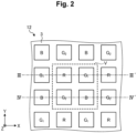
- Fig. 2 schematically illustrates the layout of the pixel layer 3 in a planar view.
- the pixel layer 3 is a pixel array that includes a plurality of pixels arranged in the X-Y plane direction.
- Each pixel includes a photoelectric conversion element.
- An example of the photoelectric conversion element is a photodiode (PD).
- PD photodiode
- Each pixel corresponds to one of the colors of red (R), green (G), and blue (B).
- R red
- G green
- B blue
- the wavelength is ⁇ 0
- an example of the wavelength band of red light 600 nm ⁇ ⁇ 0
- An example of the wavelength band of green light is 500 nm ⁇ ⁇ 0 ⁇ 600 nm.
- An example of the wavelength band of blue light is ⁇ 0 ⁇ 500 nm.
- the respective pixels are referred to as a pixel R, a pixel G 1 , a pixel G 2 , and a pixel B, so as to be distinguishable by color.
- These four pixels R, G 1 , G 2 , and B are arranged in the Bayer array, and constitute one pixel unit (color pixel unit).
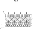
- Fig. 3 illustrates an example cross-section of the imaging device 12 as viewed from a side along the line III-III' defined in Fig. 2 .
- Fig. 4 illustrates an example cross-section of the imaging device 12 as viewed from a side along the line IV-IV' defined in Fig. 2 .
- arrows schematically indicate light entering the imaging device 12. The light that has entered travels in the negative Z-axis direction, and reaches the pixel layer 3 via the optical element 4.
- the optical element 4 condenses the red light of the incident light into the pixel R, condenses the green light into the pixel G 1 and the pixel G 2 , and condenses the blue light into the pixel B.
- Electrical charges generated in the pixel R, the pixel G 1 , the pixel G 2 , and the pixel B are converted into an electrical signal serving as a basis of a pixel signal by a transistor or the like (not illustrated), and are output to the outside of the imaging device 12 via the wiring layer 2.
- Some of the wiring lines included in the wiring layer 2 are shown in the drawings.
- the optical element 4 is provided so as to cover the pixel layer 3.
- An example of the optical element 4 is a meta-surface.
- the meta-surface includes a plurality of microstructure members (corresponding to the structure members 6 described later) having a width equal to or smaller than the wavelength of light.
- the meta-surface may have a two-dimensional structure, or may have a three-dimensional structure. It is possible to control the phase and the light intensity in accordance with the characteristics (wavelength, polarization, and incident angle) of light, simply by changing the parameters of the microstructure members. In the case of a three-dimensional structure, the degree of freedom in design is higher than that in a two-dimensional structure.
- the optical element 4 has two functions, which are a color separation function and a lens function.
- the color separation function is a function (a spectral function, or a light separation function) of separating incident light into light beams of the respective colors (respective wavelength bands).
- the lens function is a function of condensing light beams of the respective colors into the corresponding pixels. In this example, incident light is separated into red light, green light, and blue light by the color separation function. By the lens function, the red light is condensed into the pixel R, the green light is condensed into the pixel G 1 and the pixel G 2 , and the blue light is condensed into the pixel B.
- the optical element 4 includes a transparent layer 5 and structure members 6.
- the transparent layer 5 is provided on the pixel layer 3 so as to cover the pixel layer 3.
- the transparent layer 5 may have a lower refractive index than the refractive index of the structure members 6.
- An example of the material of the transparent layer 5 is SiO 2 or the like.
- the transparent layer 5 may be a void. In that case, the refractive index of the transparent layer 5 may be equal to the refractive index of air.
- the material of the transparent layer 5 may be a single material, or may be a plurality of layered materials.
- the plurality of structure members 6 is disposed on the transparent layer 5 or in the transparent layer 5, and is arranged in the plane direction (X-Y plane direction) of the transparent layer 5 in a periodic manner (with a periodic structure), for example.
- the structure members 6 are disposed on the transparent layer 5 on the opposite side (the positive Z-axis direction side) of the transparent layer 5 from the pixel layer 3.
- the plurality of structure members 6 may be arranged at regular intervals for ease of design or the like, or may be arranged at irregular intervals.
- Each structure member 6 is a nano-order-sized microstructure member having a dimension equal to or smaller than the wavelength of incident light.
- Fig. 5 schematically illustrates an example cross-section of the plurality of structure members 6 corresponding to the portion surrounded by a dashed line V in Fig. 2 .
- the plurality of structure members 6 includes a plurality of structure members 61 (first structure members), a plurality of structure members 62 (second structure members), and a plurality of structure members 63 (third structure members).
- the plurality of structure members 61 each have the same type (first type) of cross-sectional shape.
- the same type of cross-sectional shape includes cross-sectional shapes having different dimensions (lengths, widths, and the like).
- the plurality of structure members 62 each have the same type (second type) of cross-sectional shape.
- the plurality of structure members 63 each have the same type (third type) of cross-sectional shape.
- Each cross-sectional shape may be a four-fold rotationally symmetrical shape.
- Such a cross-sectional shape may include at least one of a square shape, a cross shape, and a circular shape, for example.
- the structure members 61, the structure members 62, and the structure members 63 have different types of cross-sectional shapes.
- the cross-sectional shape of a structure member 61 is a square shape.
- the cross-sectional shape of a structure member 62 is an X-like shape
- the X-like shape is an example of a shape including a cross shape, and is a shape formed by rotating a cross shape in a plane by 45°.
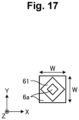
- the cross-sectional shape of a structure member 63 is a hollow rhombic shape.
- the hollow rhombic shape is an example of a shape including a square shape, and is a shape formed by rotating a hollow square shape in a plane by 45°.
- the plurality of structure members 6 disposed in the region facing the pixel G 1 (or the pixel G 2 ) has an overall layout structure that is formed by rotating the overall layout structure of the plurality of structure members 6 disposed in the region facing the pixel G 2 (or the pixel G 1 ) by 90°, as can be seen from a comparison between Figs. 2 and 5 .
- the overall layout structures of the structure members 6 above the pixel G 1 are the same as those above the pixel G 2 except for being rotated 90°, it is possible to efficiently condense light even in a complicated color layout such as a Bayer array.
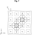
- Figs. 6 to 8 are diagrams schematically illustrating light condensing into the corresponding pixel.
- blue light is condensed into the pixel B.
- the plurality of structure members 6 Figs. 3 to 5
- the plurality of structure members 6 is disposed so that, of the light that has entered the outside of the region facing the pixel B, the light of the color corresponding to the pixel B is condensed into the pixel B.
- the amount of received light can be made larger than that in a case where only the light that has entered the region facing the pixel B is condensed into the pixel B.
- green light is condensed into the pixel G 1 and the pixel G 2 .
- the plurality of structure members 6 is disposed so that, of the light that has entered the outside of the regions facing the pixel G 1 and the pixel G 2 , the light of the color corresponding to the pixel G 1 and the pixel G 2 is condensed into the pixel G 1 and the pixel G 2 .
- the amount of received light can be made larger than that in a case where only the light that has entered the regions facing the pixel G 1 and the pixel G 2 is condensed into the pixel G 1 and the pixel G 2 .
- red light is condensed into the pixel R.
- the plurality of structure members 6 is disposed so that, of the light that has entered the outside of the region facing the pixel R, the light of the color corresponding to the pixel R is condensed into the pixel R.
- the amount of received light can be made larger than that in a case where only the light that has entered the region facing the pixel R is condensed into the pixel R.
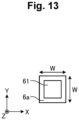
- Figs. 12 to 17 are diagrams illustrating an example schematic configuration of a structure member.
- Figs. 12 and 13 illustrate example schematic configurations of a structure member 61 in a side view and a planar view.
- Figs. 14 and 15 illustrate example schematic configurations of a structure member 62 in a side view and a planar view.
- Figs. 16 and 17 illustrate example schematic configurations of a structure member 63 in a side view and a planar view.
- the structure member 61, the structure member 62, and the structure member 63 will be referred to simply as "the structure members 61 and the like" in some cases.
- Each of the structure members 61 and the like is a columnar structure member extending in a Z-axis direction, and is formed on a base portion 6a.
- An example of the material of the columnar structure members is TiO 2 (the refractive index being 2.40) or SiN (the refractive index being 2.05).
- the base portions 6a constitute a transparent layer below the columnar structure member.
- Each base portion 61a is part of a SiO 2 substrate (the refractive index being 1.45), for example. Air exists on the sides and the upper side of each of the structure members 61 and the like.
- the width of the base portion 6a corresponding to each of the structure members 61 and the like is referred to and shown as the width W.
- the width W of each base portion 6a defines the layout cycles of the structure members 61 and the like.
- the width W may be set to W ⁇ ( ⁇ min /n 2 ) so that diffracted light is not generated on the transmission side.
- ⁇ min represents the shortest wavelength in the wavelength band of the light reception target, and is 410 nm, for example.
- An example of the width W (the layout cycle of each of the structure members 61 and the like) is 280 nm.
- the height (the length in a Z-axis direction) of each of the structure members 61 and the like in a side view is referred to and shown as the height H.
- the heights H of the structure members 61 and the like may be the same.
- the height H may be set to H ⁇ ⁇ r / (n 1 - n 0 ) so that the structure members 61 and the like can give an optical phase delay amount (a phase value) of 2 ⁇ or larger to incident light, which is light traveling in the Z-axis direction.
- the wavelength ⁇ r is a desired center wavelength in the wavelength band on the longest wavelength side among the wavelength bands of light to be subjected to color separation.
- n 1 represents the refractive index of the structure members 61 and the like.
- n 1 2.40
- the height H is 1250 nm, for example.
- n 1 2.05
- the height H is 1600 nm, for example.
- the cross-sectional shapes of the structure members 61 and the like are designed (including the dimensional design), so that various combinations capable of giving different optical phase delay amounts to light of the respective colors (light of the respective wavelengths) can be obtained. As various cross-sectional shapes are designed, the number of combinations increases, and the degree of freedom in design becomes even higher.
- Figs. 18 and 19 are diagrams illustrating examples of combinations of the respective wavelengths and optical phase delay amounts.
- the square plots indicate the optical phase delay amounts when the dimensions of the cross-sectional shapes of the structure members 61 each having a square cross-sectional shape are set to various values.
- the X-like plots indicate the optical phase delay amounts when the dimensions of the cross-sectional shapes of the structure members 62 each having an X-like cross-sectional shape are set to various values.
- the rhombic plots indicate the optical phase delay amounts when the dimensions of the cross-sectional shapes of the structure members 63 each having a hollow rhombic cross-sectional shape are set to various values. In any of these cases, the heights H are the same.
- the black circle plots indicate ideal optical phase delay amounts in the lens designs that will be described later.
- Fig. 18 illustrates the optical phase delay amounts in a case where the structure members 61 and the like are formed with TiO 2 .
- Fig. 19 illustrates the optical phase delay amounts in a case where the structure members 61 and the like are formed with SiN.
- the cross-sectional shapes of the structure members 61 and the like it is possible to obtain various combinations of light of the respective colors (light of the respective wavelengths) and optical phase delay amounts. That is, simply by using columnar structure members having the same height H, it is possible to obtain optical phase delay amount characteristics (phase characteristics) having various wavelength dispersions. This is because the optical waveguide mode and the optical resonance mode to be generated, and the wavelength dispersion characteristics of the optical phase delay amounts to be generated by the optical waveguide mode and the optical resonance mode can change with cross-sectional shapes.
- lens designing is possible not only in a case where the number of wavelengths is three but also in a case where the number of wavelengths is two or four or even more.
- the cross-sectional shapes and the layout of the structure members 61 and the like are designed so as to achieve an ideal optical phase delay amount distribution (a phase distribution).
- the cross-sectional shapes and the layout of the structure members 61 and the like are designed in accordance with an ideal optical phase delay amount distribution for each center wavelength of the wavelength bands of red light, green light, and blue light.
- the size of a pixel is 1.68 um ⁇ 1.68 um.
- the focal length is 4.2 um.
- the center wavelength corresponding to blue light is 430 nm.
- the center wavelength corresponding to green light is 520 nm.
- the center wavelength corresponding to red light is 635 m.
- ⁇ d represents the center wavelength (designed wavelength).
- X f , Y f , and Z f represent condensing positions.
- n 2 represents the refractive index of the base portion 6a.
- C is an arbitrary constant.
- ⁇ is converted so as to fall within the range of 0 to 2 ⁇ .
- -0.5 ⁇ and 2.5 ⁇ are converted into 1.5 ⁇ and 0.5 ⁇ , respectively.
- the boundary regions of the optical phase delay amount distribution at each center wavelength is set so that the optical phase delay amount distribution (including the adjacent lenses) is horizontally and vertically symmetrical about the condensing position.
- the constant C may be optimized so that the error (the difference from the ideal value) of the optical phase delay amount distribution is minimized at each wavelength. From the optical phase delay amount at each wavelength, a structure most suitable for the optical phase delay amount distribution at each center wavelength (a structure with the smallest error) is disposed at the corresponding position.
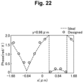
- Figs. 20 to 29 illustrate examples of lens designing in a case where the structure members 61 and the like are formed with TiO 2 .
- a plurality of structure members 61 and the like is disposed.
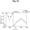
- Fig. 21 illustrates an ideal optical phase delay amount distribution (Phase (rad/ ⁇ )) in a case where the center wavelength is 430 nm (blue light).
- a dashed line (Ideal) indicates an ideal optical phase delay amount distribution, and plots (Designed) indicate an optical phase delay amount distribution obtained with the layout of the plurality of the structure members 61 and the like illustrated in Fig. 20 described above.
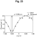
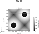
- Fig. 24 illustrates an ideal optical phase delay amount distribution in a case where the center wavelength is 520 nm (green light).
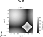
- Fig. 27 illustrates an ideal optical phase delay amount distribution in a case where the center wavelength is 635 nm (red light).
- an optical phase delay amount distribution close to an ideal one is obtained at any of the center wavelengths of 430 nm, 520 nm, and 635 nm (blue light, green light, and red light).
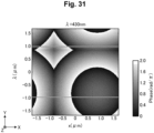
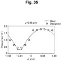
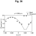
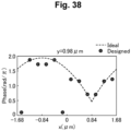
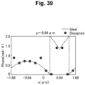
- Figs. 30 to 39 illustrate examples of lens designing in a case where the structure members 61 and the like are formed with SiN. As illustrated in Fig. 30 , a plurality of structure members 61 and the like is disposed.
- Fig. 31 illustrates an ideal optical phase delay amount distribution in a case where the center wavelength is 430 nm (blue light).
- Fig. 34 illustrates an ideal optical phase delay amount distribution in a case where the center wavelength is 520 nm (green light).
- Fig. 37 illustrates an ideal optical phase delay amount distribution in a case where the center wavelength is 635 nm (red light).
- an optical phase delay amount distribution close to an ideal one is obtained at any of the center wavelengths of 430 nm, 520 nm, and 635 nm (blue light, green light, and red light).
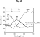
- Fig. 40 illustrates an example of the spectrums of light entering the respective pixels in a case where the structure members 61 and the like are formed with TiO 2 .
- the spectrums are the spectrums observed when unpolarized planar light waves are made to enter perpendicularly to the substrate (the X-Y plane).
- the distance from the lower end (the lens structure end) of the structure members 61 and the like to the pixel layer 3 is 4.2 um (the lens focal length).
- the abscissa axis of the graph indicates wavelength (nm).
- the ordinate axis indicates light reception efficiency (detected power).
- Light reception efficiency is "light intensity on pixels"/"intensity of light entering the structure members 61 and the like). For example, when half of the light that has entered the structure members 61 and the like enters the pixels, the light reception efficiency is 0.5.
- the spectrum of light entering a pixel R is indicated by a graph line R.
- the spectrums of light entering a pixel G 1 and a pixel G 2 are indicated by a graph line G 1 and a graph line G 2 .
- the spectrum of light entering a pixel B is indicated by a graph line B.
- the pixel R, the pixel G 1 , the pixel G 2 , and the pixel B each have a peak value greater than the upper limit value of 0.2 of the comparative example, and the amount of received light in the pixels is larger than that in the comparative example.
- the light reception efficiency of the pixel B greatly exceeds the upper limit value of 0.2 of the comparative example.
- the light reception efficiency of the pixel G 1 and the pixel G 2 greatly exceeds the upper limit value of 0.2 of the comparative example.
- the light reception efficiency of the pixel R greatly exceeds the upper limit value of 0.2 of the comparative example.
- the value obtained by averaging the total transmittance, which is "the sum of the light intensities in all the pixels"/"the intensity of light entering the structure members 61 and the like" over the wavelength range of 400 nm to 700 nm is 93.2%, which greatly exceeds the upper limit value up to 33% in a case where conventional filters are used. This also shows that the light reception efficiency of the pixels can be increased.
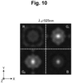
- Fig. 41 illustrates an intensity distribution of light (blue light) having the wavelength indicated by the marker MA in Fig. 40 . It can be seen that the distribution concentrates in the pixel B.
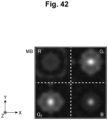
- Fig. 42 illustrates an intensity distribution of light (green light) having the wavelength indicated by the marker MB in Fig. 40 . It can be seen that the distribution concentrates in the pixel G 1 and the pixel G 2 .
- Fig. 43 illustrates an intensity distribution of light (red light) having the wavelength indicated by the marker MC in Fig. 40 . It can be seen that the distribution concentrates in the pixel R.
- Fig. 44 illustrates an example of the spectrums of light entering the respective pixels in a case where the structure members 61 and the like are formed with SiN.
- the pixel R, the pixel G 1 , the pixel G 2 , and the pixel B each have a peak value greater than the upper limit value of 0.2 of the comparative example, and the amount of received light in the pixels is larger than that in the comparative example, as in the above-described case where the structure members 61 and the like are formed with SiO 2 .
- the total transmittance is 97.1%, which greatly exceeds the upper limit value up to 33% in a case where conventional filters are used.
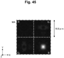
- Fig. 45 illustrates an intensity distribution of light (blue light) having the wavelength indicated by the marker MA in Fig. 44 . It can be seen that the distribution concentrates in the pixel B.
- Fig. 46 illustrates an intensity distribution of light (green light) having the wavelength indicated by the marker MB in Fig. 44 . Note that the wavelength indicated by the marker MB in this case with SiN is 520 nm. It can be seen that the distribution concentrates in the pixel G 1 and the pixel G 2 .
- Fig. 47 illustrates an intensity distribution of light (red light) having the wavelength indicated by the marker MC in Fig. 44 . It can be seen that the distribution concentrates in the pixel R.
- Figs. 48 to 66 are diagrams illustrating examples of incident angle dependences.
- Figs. 48 to 58 illustrate examples of incident angle dependences in cases where the structure members 61 and the like are formed with TiO 2 .
- a pixel R, a pixel G 1 , a pixel G 2 , and a pixel B are disposed as illustrated in Fig. 48 .
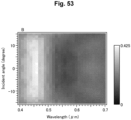
- Figs. 50 to 53 illustrate the incident angle dependences in cases where the angle in the X-Z plane with the Z-axis direction set to 0° is set as the incident angle at this time as illustrated in Fig. 49 .
- Fig. 50 illustrates the light reception efficiency of the pixel R as a spectrum at each wavelength ( ⁇ m) and each incident angle (degrees), or at each incident angle.
- Fig. 51 illustrates the light reception efficiency of the pixel G 1 as a spectrum at each incident angle.
- Fig. 52 illustrates the light reception efficiency of the pixel G 2 as a spectrum at each incident angle.
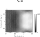
- Figs. 55 to 58 illustrate the incident angle dependences in cases where the angle in the Y-Z plane with the Z-axis direction set to 0° is set as the incident angle as illustrated in Fig. 54 .
- Fig. 55 illustrates the light reception efficiency of the pixel R as a spectrum at each incident angle.
- Fig. 56 illustrates the light reception efficiency of the pixel G 1 as a spectrum at each incident angle.
- Fig. 57 illustrates the light reception efficiency of the pixel G 2 as a spectrum at each incident angle.
- Fig. 58 illustrates the light reception efficiency of the pixel B as a spectrum at each incident angle. In any of the pixel R, the pixel G 1 , the pixel G 2 , and the pixel B, no significant change occurs in the spectrum over the range of about ⁇ 12° in incident angle.
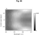
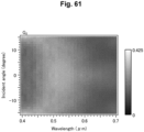
- Figs. 59 to 66 illustrate examples of incident angle dependences in cases where the structure members 61 and the like are formed with SiN.
- Figs. 59 to 62 illustrate the incident angle dependences in the X-Z plane as illustrated in Fig. 49 described above.
- Fig. 59 illustrates the dependence on the incident angle to the pixel R.
- Fig. 60 illustrates the dependence on the incident angle to the pixel G 1 .
- Fig. 61 illustrates the dependence on the incident angle to the pixel G 2 .
- Fig. 62 illustrates the dependence on the incident angle to the pixel B. In any of the pixels, no significant change occurs in the spectrum over the range of about ⁇ 12° in incident angle.
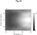
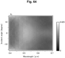
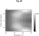
- Figs. 63 to 66 illustrate the incident angle dependences in the Y-Z plane as illustrated in Fig. 54 described above.
- Fig. 63 illustrates the dependence on the incident angle to the pixel R.
- Fig. 64 illustrates the dependence on the incident angle to the pixel G 1 .
- Fig. 65 illustrates the dependence on the incident angle to the pixel G 2 .
- Fig. 66 illustrates the dependence on the incident angle to the pixel B. In any of the pixels, no significant change occurs in the spectrum over the range of about ⁇ 12° in incident angle.
- the incident angle has a tolerance of at least ⁇ 12°. This means that, even in a case where an image is captured with an imaging lens having a numerical aperture (NA) up to 0.21, for example, a color error is less likely to occur.
- NA numerical aperture
- the optical element 4 according to the embodiment can also be used in a smartphone camera or the like. Note that the tolerance for incident angle mainly depends on the focal length, and thus, the allowable range of angles becomes even wider if a lens having a shorter focal length is designed.
- an imaging device includes filters (for example, color filters) in place of the optical element 4. That is, filters corresponding to the colors of the respective pixels are provided so as to cover the corresponding pixels. In this case, light having any wavelength outside the transmission wavelength band is absorbed by the filters, only about 1/3 of the amount of light that has entered the filters remains after transmission through the filters, and therefore, the light reception efficiency becomes lower.
- the imaging device 12 according to the embodiment a larger amount (90% or more, for example) of light is maintained as described above, and thus, the light reception efficiency is greatly increased.
- microlenses are provided (integrated) on the opposite side of the filters from the pixels, to increase the amount of received light (or to increase sensitivity) by improving the aperture ratio, reducing the dependence on the light incident angle, and the like.
- a two-layer structure formed at least with filters and microlenses is formed. Therefore, the structure becomes complicated, and the manufacturing costs also increase.
- the optical element 4 according to the embodiment a color separation function and a lens function can be obtained only with the optical element 4. Accordingly, the structure can be simplified, and the manufacturing costs can be lowered.
- the plurality of structure members 6 can be disposed in a plane (X-Y plane) without gaps. Thus, the aperture ratio becomes higher than that of microlenses.
- the signal processing unit 13 of the imaging apparatus 10 generates a pixel signal on the basis of an electrical signal obtained from the imaging device 12. To obtain the electrical signal, the signal processing unit 13 also controls the imaging device 12. Controlling the imaging device 12 includes exposure of the pixels of the imaging device 12, conversion of charges accumulated in the pixel layer 3 into an electrical signal, reading of the electrical signal, and the like.
- the plurality of structure members 6 is provided on the transparent layer 5 on the side opposite from the pixel layer 3, with the transparent layer 5 interposed in between.
- the configuration of the transparent layer 5 and the plurality of structure members 6 is not limited to this.
- Figs. 67 and 68 are diagrams illustrating example schematic configurations of imaging devices according to modifications.
- the plurality of structure members 6 is provided in the transparent layer 5 in an optical element 4A.
- the structure members 6 are buried in the transparent layer 5 (on the PDs) on the pixel layer 3.
- the transparent layer 5 in an optical element 4B includes a transparent substrate 5a and an air layer 5b.
- the plurality of structure members 6 is provided on the transparent substrate 5a (supported by the transparent substrate 5a), so as to extend from the transparent substrate 5a toward the pixel layer 3 (in the negative Z-axis direction).
- Fig. 69 is a diagram illustrating examples of cross-sectional shapes of the structure members.
- the structure members 6 may have various cross-sectional shapes as illustrated in the drawing.
- the example shapes are four-fold rotationally symmetrical shapes obtained by combining square shapes, cross shapes, and circular shapes in various manners.
- the imaging device may include filters.
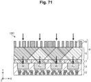
- Figs. 70 and 71 are diagrams illustrating an example schematic configuration of an imaging device according to such a modification.
- An imaging device 12C illustrated in the drawings includes a filter layer 7 disposed between the pixel layer 3 and the optical element 4.
- Fig. 70 illustrates an example cross-section of the imaging device 12C as viewed from a side along the line III-III', in a case where the imaging device 12 is replaced with the imaging device 12C in Fig. 2 .
- Fig. 71 illustrates an example cross-section of the imaging device 12C as viewed from a side along the line IV-IV', in a case where the imaging device 12 is replaced with the imaging device 12C in Fig. 2 .
- the filter layer 7 includes a filter 7R, a filter 7G 1 , a filter 7G 2 , and a filter 7B.
- the filter 7R is provided so as to cover a pixel R, and allows red light to pass.
- the filter 7G 1 is provided so as to cover a pixel G 1 , and allows green light to pass.
- the filter 7G 2 is provided so as to cover a pixel G 2 , and allows green light to pass.
- the filter 7B is provided so as to cover a pixel B, and allows blue light to pass. Examples of the material of the filter 7R, the filter 7G 1 , the filter 7G 2 , and the filter 7B include organic materials such as resin.
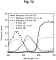
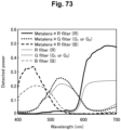
- Figs. 72 and 73 are diagrams illustrating examples of the spectrums of light entering the pixels.
- Fig. 72 illustrates an example of the spectrums in a case where the structure members 61 and the like are formed with TiO 2 .
- the light reception efficiency of the pixel R is indicated by a graph line "Metalens ⁇ R filter (R)".
- the light reception efficiency of the pixel G 1 and the pixel G 2 is indicated by a graph line "Metalens ⁇ G filter (G 1 or G 2 )".
- the light reception efficiency of the pixel B is indicated by a graph line "Metalens ⁇ R filter (B)”.
- the light reception efficiency of the pixel R in a case where the optical element 4 is not provided but only conventional filters are provided is indicated by a graph line "R filter (R)".
- the light reception efficiency of the pixel G is indicated by a graph line "G filter (G 1 or G 2 )”.
- the light reception efficiency of the pixel B is indicated by a graph line "B filter (B)”.
- the peak values of the spectrums of the pixel R, the pixel G 1 , the pixel G 2 , and the pixel B are about 1.2 to 2.0 times greater than those in the comparative example, and a higher light reception efficiency than that in the comparative example can be obtained. Also, the total transmittance is 43.3%, which is much higher (about 1.25 times higher) than 34.7% of the comparative example. Further, the spectrum of light entering each pixel is also sharper than the spectrum in the comparative example, and it is also apparent that other unnecessary color components can be reduced accordingly. Thus, color reproducibility is increased.
- Fig. 73 illustrates an example of the spectrums in a case where the structure members 61 and the like are formed with SiN.
- the peak values of the spectrums of the pixel R, the pixel G 1 , the pixel G 2 , and the pixel B are about 1.2 to 2.0 times greater than those in the comparative example, and a higher light reception efficiency than that in the comparative example can be obtained.
- the total transmittance is 45%, which is much higher (about 1.30 times higher) than 34.7% of the comparative example.
- the spectrum of light entering each pixel is also sharper than the spectrum in the comparative example, and it is also apparent that other unnecessary color components can be reduced accordingly. Thus, color reproducibility is increased.
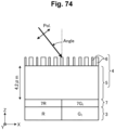
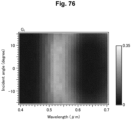
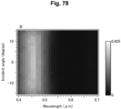
- Figs. 74 to 91 illustrate examples of incident angle dependences in cases where the structure members 6 are formed with TiO 2 .
- Figs. 75 to 78 illustrate the incident angle dependences in the X-Z plane as illustrated in Fig. 74 .
- Fig. 75 illustrates the dependence on the incident angle to the pixel R.
- Fig. 76 illustrates the dependence on the incident angle to the pixel G 1 .
- Fig. 77 illustrates the dependence on the incident angle to the pixel G 2 .
- Fig. 78 illustrates the dependence on the incident angle to the pixel B. In any of the pixels, no significant change occurs in the spectrum over the range of about ⁇ 12° in incident angle.
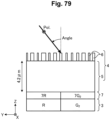
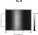
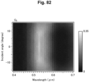
- Figs. 80 to 83 illustrate the incident angle dependences in the Y-Z plane as illustrated in Fig. 79 .
- Fig. 80 illustrates the dependence on the incident angle to the pixel R.
- Fig. 81 illustrates the dependence on the incident angle to the pixel G 1 .
- Fig. 82 illustrates the dependence on the incident angle to the pixel G 2 .
- Fig. 83 illustrates the dependence on the incident angle to the pixel B. In any of the pixels, no significant change occurs in the spectrum over the range of about ⁇ 12° in incident angle.
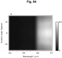
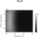
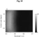
- Figs. 84 to 91 illustrate examples of incident angle dependences in cases where the structure members 61 and the like are formed with SiN.
- Figs. 84 to 87 illustrate the incident angle dependences in the X-Z plane as illustrated in Fig. 74 described above.
- Fig. 84 illustrates the dependence on the incident angle to the pixel R.
- Fig. 85 illustrates the dependence on the incident angle to the pixel G 1 .
- Fig. 86 illustrates the dependence on the incident angle to the pixel G 2 .
- Fig. 87 illustrates the dependence on the incident angle to the pixel B. In any of the pixels, no significant change occurs in the spectrum over the range of about ⁇ 12° in incident angle.
- Figs. 88 to 91 illustrate the incident angle dependences in the Y-Z plane as illustrated in Fig. 79 described above.
- Fig. 88 illustrates the dependence on the incident angle to the pixel R.
- Fig. 89 illustrates the dependence on the incident angle to the pixel G 1 .
- Fig. 90 illustrates the dependence on the incident angle to the pixel G 2 .
- Fig. 91 illustrates the dependence on the incident angle to the pixel B. In any of the pixels, no significant change occurs in the spectrum over the range of about ⁇ 12° in incident angle.
- the imaging device 12C further including the filter layer 7
- light reception efficiency can be increased, and color reproducibility can also be further increased.
- TiO 2 and SiN have been described as examples of the material of the structure members 6.
- the material of the structure members 6 is not limited those.
- SiC, TiO 2 , GaN, or the like, other than SiN may be used as the material of the structure members 6. Any of these materials is suitable, because the refractive index is high, and the absorption loss is low.
- Si, SiC, SiN, TiO 2 , GaAs, GaN, or the like may be used as the material of the structure members 6.
- any of these materials is suitable, having a low loss.
- InP or the like can be used as the material of the structure members 6, in addition to the above-described materials.
- examples of the material include polyimides such as fluorinated polyimides, benzocyclobutene (BCB), photocurable resins, UV epoxy resins, acrylic resins such as PMMA, and polymers such as resists in general.
- polyimides such as fluorinated polyimides, benzocyclobutene (BCB), photocurable resins, UV epoxy resins, acrylic resins such as PMMA, and polymers such as resists in general.
- the materials of the transparent layer 5 are not limited to those. Any materials, including a general glass material and the like, may be used as long as each of the materials has a lower refractive index than the refractive index of the material of the structure members 6, and has a low loss at the wavelength of incident light.
- the transparent layer 5 is only required to have a sufficiently low loss at the wavelength of the light to reach the corresponding pixel. Therefore, the transparent layer 5 may be formed with the same material as the color filters, and may be formed with an organic material such as resin, for example.
- the transparent layer 5 is not only formed with a material similar to that of the color filters, but also may have a structure similar to that of the color filters, and may be designed to have absorption characteristics corresponding to the wavelength of the light to be guided to the corresponding pixel.
- the three primary colors of RGB have been described as an example of the corresponding colors of the pixels.
- the pixels may also correspond to light of wavelengths (such as infrared light, ultraviolet light, and the like, for example) other than the three primary colors.
- structure members having cross-sectional shapes of three different types which are the structure members 61, the structure members 62, and the structure members 63.
- structure members of two types for example, only the structure members 61 and the structure members 62
- structure members of four or more types may be used.
- the optical element 4 includes the transparent layer 5 for covering a plurality of pixels (the pixel R and others) each including a photoelectric conversion element, and the plurality of structure members 6 that is disposed on the transparent layer 5 or in the transparent layer 5 in the plane direction (X-Y plane direction) of the transparent layer 5.
- the plurality of structure members 6 is arranged so as to condense the colors (red, green, and blue, for example) corresponding to the respective pixels of the plurality of pixels into the corresponding pixels, the colors being of incident light.
- the plurality of structure members 6 include structure members (the structure members 61, the structure members 62, and the structure members 63, for example) that have cross-sectional shapes of different types (a square shape, an X-like shape, and a hollow rhombic shape, for example) when the transparent layer 5 is viewed in a planar view (when viewed in the Z-axis direction).
- the optical element 4 described above has both a color separation function and a lens function (a light condensing function). Accordingly, the light reception efficiency of the pixels can be made much higher, and the light sensitivity can be made higher than those in a case where filters (color filter, for example) corresponding to the respective pixels are provided, and microlenses are further provided, for example. As the structure is simplified, the manufacturing costs can also be lowered. As the plurality of structure members 6 can be disposed in a plane without gaps, the aperture ratio also becomes higher than that of microlenses.
- each structure member of the plurality of structure members 6 may be a columnar structure member that has a higher refractive index than the refractive index of the transparent layer 5, and gives incident light an optical phase delay amount corresponding to the cross-sectional shape.
- the plurality of structure members 6 may be arranged in accordance with the optical phase delay amount distribution for realizing the above light condensing. For example, both the color separation function and the lens function can be obtained with such a layout of the plurality of structure members 6.
- each structure member of the plurality of structure members 6 may be a four-fold rotationally symmetrical shape. With this arrangement, polarization dependence can be prevented from occurring.
- the plurality of structure members 6 may be arranged so that, of light entering the outside of the region facing one pixel, light of the color corresponding to the one pixel is also condensed into the one pixel.
- the amount of received light can be made larger than that in a case where only the light that has entered the region facing one pixel is condensed into the pixel.
- the plurality of pixels includes a pixel unit that is formed with one pixel R corresponding to red, two pixels G 1 and G 2 corresponding to green, and one pixel B corresponding to blue that are arranged in a Bayer array.
- a plurality of structure members 6 disposed in the region facing one (the pixel G 1 , for example) of the pixels corresponding to green in the pixel unit has an overall layout structure formed by rotating 90° the overall layout structure of a plurality of structure members disposed in the region facing the other one (the pixel G 2 , for example) of the pixels corresponding to green.
- the overall layout structures of a plurality of structure members 6 are made the same except for being rotated 90°, it is possible to efficiently condense light even in a complicated color layout such as a Bayer array.
- the imaging device 12 described with reference to Figs. 1 to 5 and others is also an aspect of the present disclosure.
- the imaging device 12 includes the optical element 4 and a plurality of pixels (the pixel R and others) covered with the transparent layer 5. With this configuration, the manufacturing costs can be lowered as described above. Light sensitivity can also be increased, and the aperture ratio can be made higher.
- the imaging device 12C may include the filter layer 7 disposed between the plurality of pixels (the pixel R and the like) and the transparent layer 5.
- the filter layer 7 disposed between the plurality of pixels (the pixel R and the like) and the transparent layer 5.
- the imaging apparatus 10 described with reference to Fig. 1 and others is also an aspect of the present disclosure.
- the imaging apparatus 10 includes the imaging device 12 described above, and the signal processing unit 13 that generates an image signal on the basis of a pixel signal based on an electrical signal obtained from the imaging device 12. With this configuration, the manufacturing costs can be lowered as described above. Light sensitivity can also be increased, and the aperture ratio can be made higher.
Landscapes
- Physics & Mathematics (AREA)
- General Physics & Mathematics (AREA)
- Optics & Photonics (AREA)
- Multimedia (AREA)
- Signal Processing (AREA)
- Engineering & Computer Science (AREA)
- Solid State Image Pick-Up Elements (AREA)
- Optical Filters (AREA)
- Optical Elements Other Than Lenses (AREA)
- Diffracting Gratings Or Hologram Optical Elements (AREA)
- Transforming Light Signals Into Electric Signals (AREA)
- Chemical & Material Sciences (AREA)
- Crystallography & Structural Chemistry (AREA)
- Color Television Image Signal Generators (AREA)
Applications Claiming Priority (1)
| Application Number | Priority Date | Filing Date | Title |
|---|---|---|---|
| PCT/JP2020/044560 WO2022113362A1 (fr) | 2020-11-30 | 2020-11-30 | Élément optique, élément d'imagerie et dispositif d'imagerie |
Publications (3)
| Publication Number | Publication Date |
|---|---|
| EP4242702A1 true EP4242702A1 (fr) | 2023-09-13 |
| EP4242702A4 EP4242702A4 (fr) | 2024-07-17 |
| EP4242702B1 EP4242702B1 (fr) | 2026-04-15 |
Family
ID=81754186
Family Applications (1)
| Application Number | Title | Priority Date | Filing Date |
|---|---|---|---|
| EP20963625.7A Active EP4242702B1 (fr) | 2020-11-30 | 2020-11-30 | Élément optique, élément d'imagerie et dispositif d'imagerie |
Country Status (6)
| Country | Link |
|---|---|
| US (1) | US20240006440A1 (fr) |
| EP (1) | EP4242702B1 (fr) |
| JP (2) | JP7574859B2 (fr) |
| KR (1) | KR102801187B1 (fr) |
| CN (1) | CN116529637B (fr) |
| WO (1) | WO2022113362A1 (fr) |
Families Citing this family (6)
| Publication number | Priority date | Publication date | Assignee | Title |
|---|---|---|---|---|
| WO2022113363A1 (fr) * | 2020-11-30 | 2022-06-02 | 日本電信電話株式会社 | Élément optique, élément d'imagerie et dispositif d'imagerie |
| WO2025070228A1 (fr) * | 2023-09-27 | 2025-04-03 | ソニーセミコンダクタソリューションズ株式会社 | Dispositif de détection de lumière |
| US20250151435A1 (en) * | 2023-11-03 | 2025-05-08 | Visera Technologies Company Limited | Solid-state image sensor |
| US20250297855A1 (en) * | 2024-03-21 | 2025-09-25 | Kla Corporation | System and method for device-like overlay targets measurement |
| WO2025258002A1 (fr) * | 2024-06-12 | 2025-12-18 | Ntt株式会社 | Élément d'imagerie et dispositif d'imagerie |
| WO2026028602A1 (fr) * | 2024-07-30 | 2026-02-05 | ソニーセミコンダクタソリューションズ株式会社 | Dispositif de détection de lumière |
Family Cites Families (19)
| Publication number | Priority date | Publication date | Assignee | Title |
|---|---|---|---|---|
| WO2005101067A1 (fr) * | 2004-04-13 | 2005-10-27 | Matsushita Electric Industrial Co., Ltd. | Élément de condensation et dispositif de formation d'images à semiconducteur |
| KR100998098B1 (ko) * | 2004-06-22 | 2010-12-02 | 니폰덴신뎅와 가부시키가이샤 | 광학 재료, 광학 렌즈 및 프리즘 |
| EP1785750A1 (fr) * | 2004-09-01 | 2007-05-16 | Matsushita Electric Industrial Co., Ltd. | Élément condensateur, dispositif de mise en image à corps solide et procédé de fabrication |
| US8384818B2 (en) | 2008-06-18 | 2013-02-26 | Panasonic Corporation | Solid-state imaging device including arrays of optical elements and photosensitive cells |
| TWI424200B (zh) * | 2008-12-31 | 2014-01-21 | Ind Tech Res Inst | 色彩分離光學元件以及所應用的影像裝置 |
| CN102160180A (zh) * | 2009-07-24 | 2011-08-17 | 松下电器产业株式会社 | 摄像装置以及固体摄像元件 |
| JP2011040441A (ja) * | 2009-08-06 | 2011-02-24 | Panasonic Corp | 固体撮像装置 |
| JP2015028960A (ja) * | 2011-12-01 | 2015-02-12 | ソニー株式会社 | 固体撮像装置および電子機器 |
| US10790325B2 (en) * | 2015-07-29 | 2020-09-29 | Samsung Electronics Co., Ltd. | Imaging apparatus and image sensor including the same |
| JP7062366B2 (ja) * | 2017-03-03 | 2022-05-06 | 株式会社ジャパンディスプレイ | 表示装置、表示方法及び色分離素子 |
| JP2018207035A (ja) * | 2017-06-08 | 2018-12-27 | 凸版印刷株式会社 | 固体撮像素子 |
| JP6981496B2 (ja) | 2018-04-17 | 2021-12-15 | 日本電信電話株式会社 | カラー撮像素子および撮像装置 |
| JP6707105B2 (ja) * | 2018-04-17 | 2020-06-10 | 日本電信電話株式会社 | カラー撮像素子および撮像装置 |
| JP6857163B2 (ja) | 2018-09-26 | 2021-04-14 | 日本電信電話株式会社 | 偏光イメージング撮像システム |
| US20200301053A1 (en) * | 2019-03-20 | 2020-09-24 | Coherent AI LLC | Optical sensing device employing light intensity detectors integrated with nanostructures |
| EP3812801B1 (fr) * | 2019-10-23 | 2024-06-19 | Samsung Electronics Co., Ltd. | Capteur d'images comprenant un réseau de lentilles de séparation de couleurs et dispositif électronique comprenant le capteur d'images |
| US11640645B2 (en) * | 2019-10-25 | 2023-05-02 | Samsung Electronics Co., Ltd. | Apparatus and method of acquiring image by employing color separation lens array |
| CN114447007A (zh) | 2020-10-30 | 2022-05-06 | 三星电子株式会社 | 包括分色透镜阵列的图像传感器和包括该图像传感器的电子设备 |
| WO2022113363A1 (fr) * | 2020-11-30 | 2022-06-02 | 日本電信電話株式会社 | Élément optique, élément d'imagerie et dispositif d'imagerie |
-
2020
- 2020-11-30 KR KR1020237017916A patent/KR102801187B1/ko active Active
- 2020-11-30 EP EP20963625.7A patent/EP4242702B1/fr active Active
- 2020-11-30 JP JP2022565015A patent/JP7574859B2/ja active Active
- 2020-11-30 US US18/039,048 patent/US20240006440A1/en active Pending
- 2020-11-30 WO PCT/JP2020/044560 patent/WO2022113362A1/fr not_active Ceased
- 2020-11-30 CN CN202080107529.7A patent/CN116529637B/zh active Active
-
2024
- 2024-10-17 JP JP2024182258A patent/JP7852689B2/ja active Active
Also Published As
| Publication number | Publication date |
|---|---|
| JPWO2022113362A1 (fr) | 2022-06-02 |
| WO2022113362A1 (fr) | 2022-06-02 |
| JP7574859B2 (ja) | 2024-10-29 |
| EP4242702B1 (fr) | 2026-04-15 |
| KR102801187B1 (ko) | 2025-04-29 |
| CN116529637A (zh) | 2023-08-01 |
| EP4242702A4 (fr) | 2024-07-17 |
| JP2024180638A (ja) | 2024-12-26 |
| US20240006440A1 (en) | 2024-01-04 |
| JP7852689B2 (ja) | 2026-04-28 |
| KR20230093325A (ko) | 2023-06-27 |
| CN116529637B (zh) | 2025-05-13 |
Similar Documents
| Publication | Publication Date | Title |
|---|---|---|
| EP4242702A1 (fr) | Élément optique, élément d'imagerie et dispositif d'imagerie | |
| US11733100B2 (en) | Polarization imaging system | |
| US12155915B2 (en) | Image sensor and imaging device | |
| EP2320462B1 (fr) | Capteur d'images doté de guides d'onde formés dans les filtres de couleur | |
| JP7574860B2 (ja) | 撮像素子及び撮像装置 | |
| JP7590657B2 (ja) | 分光素子アレイ、撮像素子および撮像装置 | |
| JP7574858B2 (ja) | 撮像素子及び撮像装置 | |
| US20210091130A1 (en) | Image sensor with micro-structured color filter | |
| US20260114067A1 (en) | Optical element, image sensor and imaging device | |
| EP4212920B1 (fr) | Élément optique, élément d'imagerie et dispositif d'imagerie | |
| US9257469B2 (en) | Color imaging device | |
| WO2019063241A1 (fr) | Capteur d'image comprenant des pixels permettant d'empêcher ou de réduire l'effet de diaphonie | |
| EP4212925B1 (fr) | Élément d'imagerie et dispositif d'imagerie | |
| US12622079B2 (en) | Optical element, image sensor and imaging device for wavwlength-dependent focusing of visible and near-infrared light | |
| US12364042B2 (en) | Optical element having both color filter function and lens function, image sensor thereof and imaging device | |
| WO2025258002A1 (fr) | Élément d'imagerie et dispositif d'imagerie |
Legal Events
| Date | Code | Title | Description |
|---|---|---|---|
| STAA | Information on the status of an ep patent application or granted ep patent |
Free format text: STATUS: THE INTERNATIONAL PUBLICATION HAS BEEN MADE |
|
| PUAI | Public reference made under article 153(3) epc to a published international application that has entered the european phase |
Free format text: ORIGINAL CODE: 0009012 |
|
| STAA | Information on the status of an ep patent application or granted ep patent |
Free format text: STATUS: REQUEST FOR EXAMINATION WAS MADE |
|
| 17P | Request for examination filed |
Effective date: 20230526 |
|
| AK | Designated contracting states |
Kind code of ref document: A1 Designated state(s): AL AT BE BG CH CY CZ DE DK EE ES FI FR GB GR HR HU IE IS IT LI LT LU LV MC MK MT NL NO PL PT RO RS SE SI SK SM TR |
|
| DAV | Request for validation of the european patent (deleted) | ||
| DAX | Request for extension of the european patent (deleted) | ||
| REG | Reference to a national code |
Ref legal event code: R079 Free format text: PREVIOUS MAIN CLASS: G02B0001020000 Ipc: H01L0027146000 Ref country code: DE Ref legal event code: R079 Ref document number: 602020070611 Country of ref document: DE Free format text: PREVIOUS MAIN CLASS: G02B0001020000 Ipc: H01L0027146000 |
|
| A4 | Supplementary search report drawn up and despatched |
Effective date: 20240617 |
|
| RIC1 | Information provided on ipc code assigned before grant |
Ipc: G02B 5/20 20060101ALI20240611BHEP Ipc: G02B 5/00 20060101ALI20240611BHEP Ipc: G02B 1/02 20060101ALI20240611BHEP Ipc: H01L 27/146 20060101AFI20240611BHEP |
|
| RAP3 | Party data changed (applicant data changed or rights of an application transferred) |
Owner name: NTT, INC. |
|
| REG | Reference to a national code |
Ref country code: DE Free format text: PREVIOUS MAIN CLASS: H01L0027146000 Ref country code: DE Ref legal event code: R079 Ref document number: 602020070611 Country of ref document: DE Free format text: PREVIOUS MAIN CLASS: H01L0027146000 Ipc: H10F0039000000 |
|
| RIC1 | Information provided on ipc code assigned before grant |
Ipc: H10F 39/00 20250101AFI20251106BHEP Ipc: H10F 39/18 20250101ALI20251106BHEP |
|
| GRAP | Despatch of communication of intention to grant a patent |
Free format text: ORIGINAL CODE: EPIDOSNIGR1 |
|
| STAA | Information on the status of an ep patent application or granted ep patent |
Free format text: STATUS: GRANT OF PATENT IS INTENDED |
|
| INTG | Intention to grant announced |
Effective date: 20251217 |
|
| GRAS | Grant fee paid |
Free format text: ORIGINAL CODE: EPIDOSNIGR3 |
|
| GRAA | (expected) grant |
Free format text: ORIGINAL CODE: 0009210 |
|
| STAA | Information on the status of an ep patent application or granted ep patent |
Free format text: STATUS: THE PATENT HAS BEEN GRANTED |
|
| AK | Designated contracting states |
Kind code of ref document: B1 Designated state(s): AL AT BE BG CH CY CZ DE DK EE ES FI FR GB GR HR HU IE IS IT LI LT LU LV MC MK MT NL NO PL PT RO RS SE SI SK SM TR |
|
| REG | Reference to a national code |
Ref country code: CH Ref legal event code: F10 Free format text: ST27 STATUS EVENT CODE: U-0-0-F10-F00 (AS PROVIDED BY THE NATIONAL OFFICE) Effective date: 20260415 |