EP4242719A2 - Dispositif de reproduction multi-ouverture, système de reproduction et procédé de fourniture d'un dispositif de reproduction multi-ouverture - Google Patents
Dispositif de reproduction multi-ouverture, système de reproduction et procédé de fourniture d'un dispositif de reproduction multi-ouverture Download PDFInfo
- Publication number
- EP4242719A2 EP4242719A2 EP23173334.6A EP23173334A EP4242719A2 EP 4242719 A2 EP4242719 A2 EP 4242719A2 EP 23173334 A EP23173334 A EP 23173334A EP 4242719 A2 EP4242719 A2 EP 4242719A2
- Authority
- EP
- European Patent Office
- Prior art keywords
- image
- optical
- view
- imaging device
- aperture imaging
- Prior art date
- Legal status (The legal status is an assumption and is not a legal conclusion. Google has not performed a legal analysis and makes no representation as to the accuracy of the status listed.)
- Granted
Links
Images













Classifications
-
- G—PHYSICS
- G02—OPTICS
- G02B—OPTICAL ELEMENTS, SYSTEMS OR APPARATUS
- G02B26/00—Optical devices or arrangements for the control of light using movable or deformable optical elements
- G02B26/08—Optical devices or arrangements for the control of light using movable or deformable optical elements for controlling the direction of light
- G02B26/0816—Optical devices or arrangements for the control of light using movable or deformable optical elements for controlling the direction of light by means of one or more reflecting elements
-
- G—PHYSICS
- G02—OPTICS
- G02B—OPTICAL ELEMENTS, SYSTEMS OR APPARATUS
- G02B13/00—Optical objectives specially designed for the purposes specified below
- G02B13/001—Miniaturised objectives for electronic devices, e.g. portable telephones, webcams, PDAs, small digital cameras
-
- G—PHYSICS
- G02—OPTICS
- G02B—OPTICAL ELEMENTS, SYSTEMS OR APPARATUS
- G02B13/00—Optical objectives specially designed for the purposes specified below
- G02B13/001—Miniaturised objectives for electronic devices, e.g. portable telephones, webcams, PDAs, small digital cameras
- G02B13/0055—Miniaturised objectives for electronic devices, e.g. portable telephones, webcams, PDAs, small digital cameras employing a special optical element
- G02B13/0065—Miniaturised objectives for electronic devices, e.g. portable telephones, webcams, PDAs, small digital cameras employing a special optical element having a beam-folding prism or mirror
-
- G—PHYSICS
- G02—OPTICS
- G02B—OPTICAL ELEMENTS, SYSTEMS OR APPARATUS
- G02B27/00—Optical systems or apparatus not provided for by any of the groups G02B1/00 - G02B26/00, G02B30/00
- G02B27/64—Imaging systems using optical elements for stabilisation of the lateral and angular position of the image
- G02B27/646—Imaging systems using optical elements for stabilisation of the lateral and angular position of the image compensating for small deviations, e.g. due to vibration or shake
-
- H—ELECTRICITY
- H04—ELECTRIC COMMUNICATION TECHNIQUE
- H04N—PICTORIAL COMMUNICATION, e.g. TELEVISION
- H04N23/00—Cameras or camera modules comprising electronic image sensors; Control thereof
- H04N23/45—Cameras or camera modules comprising electronic image sensors; Control thereof for generating image signals from two or more image sensors being of different type or operating in different modes, e.g. with a CMOS sensor for moving images in combination with a charge-coupled device [CCD] for still images
-
- H—ELECTRICITY
- H04—ELECTRIC COMMUNICATION TECHNIQUE
- H04N—PICTORIAL COMMUNICATION, e.g. TELEVISION
- H04N23/00—Cameras or camera modules comprising electronic image sensors; Control thereof
- H04N23/50—Constructional details
- H04N23/54—Mounting of pick-up tubes, electronic image sensors, deviation or focusing coils
-
- H—ELECTRICITY
- H04—ELECTRIC COMMUNICATION TECHNIQUE
- H04N—PICTORIAL COMMUNICATION, e.g. TELEVISION
- H04N23/00—Cameras or camera modules comprising electronic image sensors; Control thereof
- H04N23/50—Constructional details
- H04N23/55—Optical parts specially adapted for electronic image sensors; Mounting thereof
-
- H—ELECTRICITY
- H04—ELECTRIC COMMUNICATION TECHNIQUE
- H04N—PICTORIAL COMMUNICATION, e.g. TELEVISION
- H04N23/00—Cameras or camera modules comprising electronic image sensors; Control thereof
- H04N23/58—Means for changing the camera field of view without moving the camera body, e.g. nutating or panning of optics or image sensors
-
- H—ELECTRICITY
- H04—ELECTRIC COMMUNICATION TECHNIQUE
- H04N—PICTORIAL COMMUNICATION, e.g. TELEVISION
- H04N23/00—Cameras or camera modules comprising electronic image sensors; Control thereof
- H04N23/60—Control of cameras or camera modules
- H04N23/68—Control of cameras or camera modules for stable pick-up of the scene, e.g. compensating for camera body vibrations
-
- H—ELECTRICITY
- H04—ELECTRIC COMMUNICATION TECHNIQUE
- H04N—PICTORIAL COMMUNICATION, e.g. TELEVISION
- H04N23/00—Cameras or camera modules comprising electronic image sensors; Control thereof
- H04N23/60—Control of cameras or camera modules
- H04N23/68—Control of cameras or camera modules for stable pick-up of the scene, e.g. compensating for camera body vibrations
- H04N23/682—Vibration or motion blur correction
- H04N23/685—Vibration or motion blur correction performed by mechanical compensation
-
- H—ELECTRICITY
- H04—ELECTRIC COMMUNICATION TECHNIQUE
- H04N—PICTORIAL COMMUNICATION, e.g. TELEVISION
- H04N23/00—Cameras or camera modules comprising electronic image sensors; Control thereof
- H04N23/60—Control of cameras or camera modules
- H04N23/698—Control of cameras or camera modules for achieving an enlarged field of view, e.g. panoramic image capture
-
- H—ELECTRICITY
- H04—ELECTRIC COMMUNICATION TECHNIQUE
- H04N—PICTORIAL COMMUNICATION, e.g. TELEVISION
- H04N23/00—Cameras or camera modules comprising electronic image sensors; Control thereof
- H04N23/60—Control of cameras or camera modules
- H04N23/68—Control of cameras or camera modules for stable pick-up of the scene, e.g. compensating for camera body vibrations
- H04N23/681—Motion detection
- H04N23/6811—Motion detection based on the image signal
-
- H—ELECTRICITY
- H04—ELECTRIC COMMUNICATION TECHNIQUE
- H04N—PICTORIAL COMMUNICATION, e.g. TELEVISION
- H04N23/00—Cameras or camera modules comprising electronic image sensors; Control thereof
- H04N23/60—Control of cameras or camera modules
- H04N23/68—Control of cameras or camera modules for stable pick-up of the scene, e.g. compensating for camera body vibrations
- H04N23/681—Motion detection
- H04N23/6812—Motion detection based on additional sensors, e.g. acceleration sensors
-
- H—ELECTRICITY
- H04—ELECTRIC COMMUNICATION TECHNIQUE
- H04N—PICTORIAL COMMUNICATION, e.g. TELEVISION
- H04N23/00—Cameras or camera modules comprising electronic image sensors; Control thereof
- H04N23/60—Control of cameras or camera modules
- H04N23/68—Control of cameras or camera modules for stable pick-up of the scene, e.g. compensating for camera body vibrations
- H04N23/682—Vibration or motion blur correction
- H04N23/685—Vibration or motion blur correction performed by mechanical compensation
- H04N23/686—Vibration or motion blur correction performed by mechanical compensation with a variable apex prism
-
- H—ELECTRICITY
- H04—ELECTRIC COMMUNICATION TECHNIQUE
- H04N—PICTORIAL COMMUNICATION, e.g. TELEVISION
- H04N23/00—Cameras or camera modules comprising electronic image sensors; Control thereof
- H04N23/60—Control of cameras or camera modules
- H04N23/68—Control of cameras or camera modules for stable pick-up of the scene, e.g. compensating for camera body vibrations
- H04N23/682—Vibration or motion blur correction
- H04N23/685—Vibration or motion blur correction performed by mechanical compensation
- H04N23/687—Vibration or motion blur correction performed by mechanical compensation by shifting the lens or sensor position
Definitions
- the present invention relates to a multi-aperture imaging device, an imaging system and a method for providing a multi-aperture imaging device.
- the present invention further relates to multi-aperture imaging systems with a linear channel arrangement and small or smallest size.
- Multi-aperture imaging systems with a linear channel arrangement consist of several imaging channels, each of which only records a part of the object and contains a deflecting mirror.
- the object of the present invention is therefore to create a multi-aperture imaging device and an imaging system with a first and a second multi-aperture imaging device, which enables a compact, i.e. small installation space implementation with a high image quality.
- One finding of the present invention is to have recognized that the above object can be achieved by arranging optics with different optics in an array, so that different partial fields of view are captured by the optics. This is achieved both for the combination of single-channel total visual field detections and for a combination of a single-channel detection of a total visual field with a multi-channel detection of a total visual field by detecting several partial visual fields.
- a multi-aperture imaging device comprises an image sensor and an array of optical channels, each optical channel comprising optics for imaging at least a partial field of view of a total field of view onto an image sensor area of the image sensor.
- the multi-aperture imaging device includes a beam deflecting device for deflecting a beam path of the optical channels.
- a first optical channel of the array is designed to image a first partial field of view of a first overall field of view, with a second optical channel of the array being designed to image a second partial field of view of the first overall field of view.
- a third optical channel is designed to completely image a second overall field of view.
- a multi-aperture imaging device includes an image sensor and an array comprising at least first and second optical channels.
- Each optical channel includes optics for imaging an overall field of view onto an image sensor area of the image sensor.
- a beam deflection device is configured to jointly deflect a beam path of the optical channels.
- the optics of the first optical channel have a focal length that is at least 10% different from a focal length of the optics of the second optical channel.
- the multi-aperture imaging device are designed to completely capture an overall field of view with one optical channel and to capture a further overall field of view using a single channel or multiple channels.
- the optical channels used for this are arranged in the same array and are deflected by the same beam deflecting device. This enables the multi-aperture imaging device to be used to image different overall fields of view in combination with a beam deflection device that is effective for all channels for switching the viewing direction, so that a multiple arrangement of components can be avoided and a space-saving implementation is possible.
- the arrangement of the optical channels in the array enables precise adjustment of the channels and high-quality recordings.
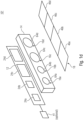
- Fig. 1a shows a schematic perspective view of a multi-aperture imaging device 10 according to an exemplary embodiment.
- the multi-aperture imaging device includes an image sensor 12 and an array 14 of optical channels 16a-e.
- Each optical channel 16a-e includes optics 64a-e for imaging at least a partial field of view of a total field of vision onto an image sensor area 24a-e of the image sensor 12.
- At least a partial field of view means that a total field of view can also be imaged using optics, as shown in FIG Fig. 1b is described.
- optical channels 16a-d of the array 14 are designed to each image a partial field of view of a first overall field of view, while a further optical channel 16e is designed to completely image a second overall field of view that is different from the first partial field of view.
- the overall visual fields are different from each other, they may partially or completely overlap.
- the overall fields of view can completely overlap but differ in size.
- the overall fields of view can also partially not overlap or even be disjoint.
- Optical channels can be understood as a course of beam paths.
- the beam paths can be influenced by the optics 64a-e arranged in the array 14, for example by scattering or focusing.
- the individual optical channels can each form a complete imaging optics and have at least one optical component or optics, such as a refractive, diffractive or hybrid lens, and can image a section of the overall object recorded with the multi-aperture imaging device.
- An aperture stop can be arranged with respect to one, several or all of the optical channels.
- the multi-aperture imaging device 10 includes a beam deflecting device 18 for deflecting a beam path of the optical channels 16a-e.
- the multi-aperture imaging device 10 is designed to capture the two overall fields of view in one position of the beam deflection device 18.
- the beam deflection device 18 is moved translationally or rotationally in order to deflect the beam paths in a different direction in the changed position, so that different overall fields of view are recorded in the changed position.
- four optical channels 16a-d are used to together image an overall field of view, a different number can also be used, such as two, at least three, at least four, at least ten, at least 20 or an even higher value.
- the array 14 is shown with all optical channels arranged in a single row, a multi-row arrangement may also be implemented in other embodiments.
- Fig. 1b shows a schematic representation of two overall fields of view 70a and 70b, which can be detected by the multi-aperture imaging device 10.
- the optics 64a-d of the optical channels 16a-d Fig. 1a configured to the To image partial visual fields 72a-d of an overall visual field 70a, whereby a different assignment or a different number of channels is also possible.
- the optics 64e of the optical channel 16a which are also arranged in the array 14, are designed to accommodate the in Fig. 1b to completely depict the overall field of view 70b shown.
- the overall field of view 70b is imaged through a single optical channel. Like it in Fig. 1b is shown, the overall field of view 70b can at least partially or completely overlap with the overall field of view 70a. Alternatively, it is also possible for the overall fields of view 70a and 70b to be at least partially different from one another.
- the overall field of view 70b can be part of the overall field of view 70a, which means that the second overall field of view can be an incomplete section of the first overall field of view or vice versa.
- the overall field of view preferably has a smaller opening angle, which can result in the imaged section of the object area in the overall field of view 70b being smaller compared to the overall field of view 70a.
- an opening angle ⁇ 1 of the field of view 70a is larger than an opening angle ⁇ 2 of the overall field of view 70b, whereby the angles can be directly related to an optical property, such as the focal lengths of the optics.
- the opening angle ⁇ 1 of the field of view 70a can be at least 10%, at least 20% or at least 50% larger than the opening angle ⁇ 2 of the field of view 70b.
- a larger opening angle leads to a shorter focal length and enables a thinner design of the optics and/or a small diameter of the optics.
- the optics 16e for capturing the overall field of view 70b can represent a telephoto lens or zoom lens or at least one provide a corresponding function, while conversely the combination of the optics 16a-d can represent a wide-angle lens compared to the optics 16e or at least provide a corresponding function.
- the optical channel 16e can be assigned its own beam deflection region 46e of the beam deflection device 18, which is different from the beam deflection regions 46a-d which are assigned to the optical channels 16a to 16d. This enables, for example, simultaneous capture of the overall visual fields 70a and 70b and thus the receipt of two images. Furthermore, for an overlap area of the overall fields of view 70a and 70b stereo or 3D information can be obtained.
- Beam deflection areas can be areas of a large-area element such as a mirror, and can be unbounded from other beam deflection areas. Alternatively, beam deflection areas can also be visibly or mechanically separated from one another, for example by forming the beam deflection areas as facets.
- the array 14 has optics 64a-d and 64e with intentionally different optical properties.
- the optics 64a-d are formed the same within manufacturing tolerances, while the optics 64e have deviations from the optics 64a-d that go beyond a level caused by manufacturing tolerances.
- the optics 64e for example, have a different focal length and/or a different opening angle than the optics 64a-d, which means that the optical properties differ from the optics 64a-d by at least 10%, at least 20% or at least 30% but also higher, for example at least 50% or even 100% or more.
- the multi-aperture imaging device 10 may include an optional electronic image stabilizer 41 to at least partially compensate for different changes obtained from one another by possible optical image stabilization or in the images obtained by relative movement between the components 12, 14 and 18.
- An image evaluation device which reads out the image sensor areas 24a-e of the multi-aperture imaging device 10 and provides overall images and which can be part of the multi-aperture imaging device 10 is, for example, designed to combine the images of the partial visual fields 72a-d into a first overall image of the overall visual field 70a, for example by means of stitching and/or or to provide a second overall image of the overall field of view 70b based on a readout of the image sensor area 24e.
- Fig. 1c show a schematic perspective view of a multi-aperture imaging device 10 ', which, compared to the multi-aperture imaging device 10, is designed to capture the overall fields of view 70a and 70b alternately, that is, alternating over time.
- the beam deflection region 46e can thus be used to alternately redirect the beam path of the optical channels 16d and 16e, resulting in an arrangement of the beam deflection region 16d Fig. 1a waived can be.
- the beam deflection region 46e can, for example, have a size that is sufficient for the deflection of the optical channel 16e imaging the entire field of view 70b, so that the deflection of the optical channel 16d used for imaging the comparatively small partial field of view 72d is also possible without any problems, as it is shown by the dashed line in the beam deflection area 46e.
- the image sensor area 24e can be used to alternately capture the overall field of view 70b and the partial field of view 72d.
- the image sensor area 24e can at least partially overlap with the image sensor area 24d or even include the image sensor area 24d, so that the image sensor area 24d does not have to be arranged separately in the overlap area and can possibly be saved.
- the multi-aperture imaging device 10' can have a switching unit 67, which is designed to provide a relative movement between the image sensor 12, the array 14 and the beam deflecting device 18, so that the optical channel 16e covers the total field of view 70b in order to capture the total field of view 70b images the image sensor area 24e through the optics 64e and, so that in order to detect the partial field of view 72d, the optical channel 16d directs the partial field of view 72d onto the image sensor, i.e. i.e., the image sensor area 24d or 24e, images through the optics 64d.
- the switching unit can include one or more actuators.
- the multi-aperture imaging device 10' may include an optical image stabilizer. This enables the synergistic use of the actuators of the optical image stabilizer as a switching device 67 or vice versa.
- the beam deflection region 46e can also be used for the deflection of the optical channel 64d, so that the beam deflection region 46d can be saved and/or that the image sensor region 24e can also be used for imaging the partial field of view 72b, so that the image sensor region 24d is saved can be. Both savings can be implemented together or individually independently of each other.
- Fig. 1a The beam deflection areas 46a-c shown can be used to alternately redirect the beam path of two optical channels.
- the optics 64e is shown as being at the edge of a row of the array 14, it may be positioned anywhere along the row or may be arranged in its own row.
- Fig. 1a image sensor areas shown 24a-c can be used to alternately image the entire field of view 70b and a partial field of view 72a-d.
- an electronic image stabilizer is used to compensate for imaging changes varying between optical channels
- two different sized overall fields of view 70a and 70b are captured by a multi-aperture imaging device, i.e. i.e., using at least one of a common image sensor 12, a common array 14 and a common beam deflection device 18, can be implemented independently of one another but also in combination with one another, so that the aspect of electronic image stabilization is an advantageous development of the aspect of the overall fields of view of different sizes represents.
- Fig. 1d shows a schematic perspective view of a multi-aperture imaging device 10" according to an exemplary embodiment.
- the multi-aperture imaging device 10" has two optical channels 16c and 16d, which have different optical properties compared to the optical channels 16a and 16b.
- This can be understood to mean that in addition to the optical channel 16e of the multi-aperture imaging device 10, which is comparable, for example, to the optical channel 64c of the multi-aperture imaging device 10", a further optical channel 64d is arranged in the multi-aperture imaging device 10", which has a comparable optical property , so that the optical channels 64c and 64d form a group of optical channels.
- the optical property of the optical channels 16c and 16d can be the same within a tolerance range of at most 10%. Likewise, the optical property of the optical channels 16a and 16b may be the same within such a tolerance range. Between the optical channels of different groups, the optical property of the optics can be increased by at least ⁇ 10% (or 1/1.1), at least ⁇ 20% (or 1/1.2) or at least ⁇ 30% (or 1/ 1.3) but also higher, for example at least ⁇ 50% (or 1/1.5) or even ⁇ 100% (or 1/2) or more from the first value of the optical property of the other group.
- the optical property of the channels can in particular be the resulting focal length of the optics present in the respective channel.
- the previously described assignment of telephoto lens and wide-angle lens can also be applicable to the groups of optical channels described, so that a group of optical channels, for example comprising the channels 16c and 16d, the zoom lens compared to the group 16a and 16b and vice versa the optical channels 16a and 16b are a wide-angle lens for the optical channels 16c and 16d.
- the optical channels 16a and 16b can form a first group of optical channels.
- the optical channels 16c and 16d can form a second group of optical channels.
- Each of the groups may be configured to capture one of the overall fields of view 70a or 70b.
- the overall field of view 70b can also be divided, as shown in FIG Fig. 1e is illustrated.
- the optical channel 16a can be designed to capture the partial field of view 72a of the overall field of view 70a.
- the optical channel 16b can be designed to capture the partial field of view 72b of the overall field of view 70a.
- the optical channel 16c can be designed to capture the partial field of view 72c of the overall field of view 70b.
- the optical channel 16d can be designed to capture the partial field of view 72d of the overall field of view 70b.
- Each of the groups of optical channels 16a/16b and 16c/16d can be designed to completely capture the associated overall field of view 70a and 70b, respectively.
- the overall field of view 70b can be an incomplete section of the overall field of view 70a.
- the overall field of view 70a can include the overall field of view 70b.
- the overall field of view 70b can completely overlap with the overall field of view 70a, but the overall field of view 70a, for example, only incompletely overlaps with the overall field of view 70b.
- each of the groups only includes two optical channels 16a and 16b or 16c and 16d, one or both groups may also include a different, higher number of optical channels, such as 3, 4, 5 or more. Also, the groups may have different numbers of optical channels, consistent with the multi-aperture imaging devices 10 and 10', which describe capture of different overall fields of view by a different number of optical channels.
- a different, higher number of groups of optical channels may also be arranged to capture a higher number of total fields of view, such as 3, 4, 5 or more.
- Each optical channel 16a-d can have an optics 64a-d for imaging a partial field of view 72a-d of a total field of view 70a or 70b onto an image sensor area 24a-d of the Image sensor 12.
- Each optical channel of the array 14 can be designed to image the partial field of view onto an image sensor area 24a-d of the image sensor assigned to the optical channel 16a-d, wherein the multi-aperture imaging device 10 "can be formed such that at least one image sensor area, which an optical channel 16c or 16d of the second group of optical channels, overlaps with an image sensor area 24a or 24b, which is assigned to an optical channel 16a or 16b of the first group of optical channels, as described in connection with Fig. 1c is described.
- the beam deflecting device 18 can be arranged to deflect a beam path 26a-d of the optical channels 16a-d.
- the first group of optical channels with at least two optical channels 16a and 16b of the array 14 is designed to each image a partial field of view 72a and 72b of the overall field of view 70a.
- the second group of optical channels with at least two optical channels 16c and 16d of the array 14 is designed to image a partial field of view 72c and 72d of the overall field of view 70b.
- multi-aperture imaging devices 10 and 10′ are applicable without restrictions to the multi-aperture imaging device 10′′, in particular the design of the beam deflection device 18 or parts thereof, which will be described later.
- an optical and/or electronic image stabilizer described herein may also be arranged .
- Fig. 1f shows a schematic perspective view of a multi-aperture imaging device 10′′′ according to an exemplary embodiment, in which the array 14 has a first optics 64a and a second optics 64b, which are alternately brought between the beam deflection device 18 and the image sensor 12 to alternately change the overall field of view 70a or 70b to be completely captured with an optical channel.
- the optics 64a and 64b have, for example, different focal lengths described above and which go beyond the manufacturing tolerances.
- the image sensor 12 can have a single image sensor area 24a.
- at least one further optional image sensor area 24b can also be provided, for example in order to capture the overall fields of view 70a and 70b simultaneously.
- the multi-aperture imaging device 10 comprises an image sensor 12 and the array 14 comprising at least a first and a second optical channel 16a and 16b.
- Each optical channel 16a and 16b includes optics 64a and 64b for imaging an overall field of view 70a and 70b on the Image sensor area 24 of the image sensor 12.
- the beam deflecting device 18 is configured to jointly deflect the beam paths of the optical channels 16a and 16b.
- the optics 64a of the first optical channel 16a has a focal length that is at least 10% of a focal length of the optics 64b of the second optical Channel 16b is different.
- further optics for imaging further overall fields of view can also be arranged on specially assigned image sensor areas or on the image sensor area 24.
- At least one overall field of view 70a, 70b or another overall field of view can be partially captured by several optical channels, as is the case with the Fig. 1a-e is to describe.
- the multi-aperture imaging device 10′′ may include an optical image stabilizer as described above and/or optionally include the electronic image stabilizer 41.
- Fig. 1g shows a schematic view of the overall fields of view 70a and 70b that can be detected by the multi-aperture imaging device 10".
- the overall field of view 70a can also be captured by means of a division into partial fields of view in order to obtain a configuration according to the multi-aperture imaging device 10.
- the overall field of view 70b can also be captured by means of a Division into partial visual fields can be recorded.
- Fig. 2a shows a schematic view of a multi-aperture imaging device 20 according to an exemplary embodiment.
- the multi-aperture imaging device 20 includes the image sensor 12, the array 14 of optical channels 16a-h, the beam deflection device 18 and an optical image stabilizer 22, such as can be used, for example, in the multi-aperture imaging device 10, 10 ', 10 "and / or 10 ".
- everyone optical channel 16a-h includes optics 64a-h for imaging a partial visual field of a total visual field onto an image sensor area 24a-h of the image sensor 12.
- optical channels 16a-e, 16g and 16h can be used to capture a total visual field with several partial visual fields, for example the optical channels 16a-e, 16g and 16h or any others, while the optical channel 16f is designed, for example, to capture the overall field of view 70b.
- the optical channels 16a-e, 16g or 16h can also be designed, in order to capture a further, ie, third or higher total field of view.
- the image sensor areas 24a-h can, for example, each be formed from a chip that includes a corresponding pixel array, wherein the image sensor areas can be mounted on a common substrate or a common circuit carrier such as a common circuit board or a common flexboard.
- the image sensor areas 24a-h can each be formed from a part of a common pixel array that extends continuously over the image sensor areas 24a-h, with the common pixel array being formed, for example, on a single chip. For example, only the pixel values of the common pixel array in the image sensor areas 24a-h are then read out.
- the beam deflecting device 18 is designed to deflect a beam path 26 of the optical channels 16a-h.
- the optical image stabilizer 22 is designed to enable optical image stabilization along a first image axis 28 and along a second image axis 32 based on a relative movement between the image sensor 12, the array 14 and the deflection device 18.
- the first image axis 28 and the second image axis 32 can be influenced by an arrangement or orientation of the image sensor areas 24a-h or the image sensor 12.
- the image axes 28 and 32 are arranged perpendicular to one another and/or correspond to extension directions of pixels of the image sensor areas 24a-d.
- the image axes 28 and 32 can alternatively or additionally indicate an orientation along which a partial field of view or the entire field of view is scanned or captured. To put it simply, the image axes 28 and 32 may be a first and second direction, respectively, in an image captured by the multi-aperture imaging device 20.
- the image axes 28 and 32 for example, have an angle of ⁇ 0° to one another, for example, they can be arranged perpendicular to one another in space.
- Optical image stabilization can be advantageous if, during a capture process during which partial visual fields or the entire visual field are captured, the multi-aperture imaging device 20 is moved relative to the object area whose field of view is captured.
- the optical image stabilizer 22 can be designed to at least partially counteract this movement in order to reduce or prevent blurring of the image.
- the optical image stabilizer 22 can be designed to generate a first relative movement 34 between the image sensor 12, the array 14 and the beam deflecting device 18.
- the optical image stabilizer 22 is designed to generate a second relative movement between the image sensor 12, the array 14 and the beam deflecting device 18.
- the optical image stabilizer 22 can comprise an actuator 36 and/or an actuator 37 for generating the relative movement 34 by displacing the array 14 or the image sensor 12 along the image axis 28.
- the actuator 36 is shown as translating or moving the array 14, according to further exemplary embodiments, the actuator 36 may alternatively or additionally be connected to the image sensor 12 and be designed to move the image sensor 12 relative to the array 14 to move.
- the optical image stabilizer can comprise an actuator 42, which is designed to generate a translational movement 39a of the beam deflecting device 18 along the image axis 28.
- the optical image stabilizer 22 is configured in such a way that it carries out the movements of the actuators 36, 37 and/or 42 so that the relative movement 34 arises between the image sensor 12, the array 14 and the beam deflection device 18. This means that even though the relative movement is 34 in Fig. 2a is shown on the array 14, other components can alternatively or additionally also be moved.
- the relative movement 34 can be carried out parallel to a line extension direction 35 and perpendicular to the beam paths 26.
- the optical image stabilizer 22 can be designed to generate or enable a rotational movement 38 of the beam deflection device 18 and/or a translational relative movement between the image sensor 12 and the array 14 along the image axis 32 and/or a translational relative movement between the array 14 and the beam deflection device 18, the actuators 36, 37 and/or 42 can be arranged for this purpose.
- the optical image stabilizer 22 can, for example, include the actuator 42, which is designed to generate the rotational movement 38.
- the optical image stabilizer 22 can be designed to generate a translational movement 39b along the image axis 32 using the actuator 42.
- optical image stabilization can be obtained along an image direction parallel thereto, for example along or opposite to the image axis 28.
- optical image stabilization can be obtained along an image direction that is arranged perpendicular to a rotation axis 44 of the rotation movement 38 in a main side plane of the image sensor 12, approximately along the image axis 32.
- a main page can be understood as a page which has a large or largest dimension compared to other pages.
- a focusing device such as that used in connection with Fig. 4 described, may be arranged, which is designed to change a focus of the multi-aperture imaging device.
- optical image stabilizer 22 In such a way that it controls the first and second relative movements as translational relative movements in order to obtain the optical image stabilization, a design of the second relative movement as a rotational movement 38 can be advantageous, since in this case a translational movement of components along the second image axis 32 can be avoided.
- This direction can be parallel to a thickness direction of the multi-aperture imaging device 20, which according to some embodiments should be kept as small as possible. Such a goal can be achieved through the rotational movement.
- the rotational movement 38 can be used to obtain the optical image stabilization along the second image axis 32.
- the translational relative movement can be arranged perpendicular to a thickness direction of the device, so that the device can be designed with a small thickness, ie thin. This offers advantages particularly in the area of mobile devices, as these can be designed with a flat housing.
- the multi-aperture imaging device 20 has the electronic image stabilizer 41, which is designed to electronically stabilize the partial images that are imaged on the image sensor areas 24a-h, that is, by manipulating the image data.
- Different methods can be used individually or in combination, such as electronic vibration reduction (e-VR), Coolpix S4, anti-shake DSP (anti-shake DSP) and/or advanced shake reduction (ASR).
- the electronic image stabilizer 41 is designed to stabilize a first partial image of the image sensor areas 24a-h of a first optical channel 16a-h of the array 14 to a first extent.
- the electronic image stabilizer 41 can be designed to additionally produce a second partial image of the image sensor areas 24a-h of another optical channel 16a-h of the array 14 in a second extent that is different from the first extent, i.e. i.e. to stabilize on a channel-specific basis.
- the other optical channel can be an optical channel with the same or comparable optical properties but also an optical channel with different optical properties, in particular the focal length.
- the scope refers to an image correction that is carried out along the first and second image axes 28 and 32, rotations about image axes and the like also being included here.
- the electronic image stabilizer 41 is designed to carry out the electronic image stabilization on a channel-specific basis for each optical channel, i.e. for each of the partial images of the image sensor areas 24a-h. This makes it possible to correct different imaging errors or even channel-specific imaging errors for the first and second optical channels 16a-h.
- the optics 64a-h of the optical channels can have optical properties that differ from one another.
- An optical property that differs from one another is obtained, for example, through manufacturing tolerances, so that the optics 64a-h differ from one another in a tolerance range of at most ⁇ 10%, at most ⁇ 5% or at most ⁇ 3% with respect to one or more optical properties, such as a focal length , a field of view angle, an optical diameter or the like.
- the different focal lengths of the channels result in different image shifts for each channel, with relative movements between the beam deflection unit and/or array and/or image sensor acting equally for all channels. This can be reduced, that is, at least partially compensated for, by electronic image stabilization combined with optical image stabilization. This should be made clear using the optical property of focal length. If there are two different values of the optical focal length in optics that are aimed at the same overall field of view, the relative movement as part of the optical image stabilization leads to the viewing axis and/or direction of the optical channels being changed equally. However, due to the different focal lengths in the optics 64a-h, the partial images in the image sensor areas 24a-h move differently, which can lead to high computing effort or even image errors when combining the partial images, stitching.
- the array 14 can, for example, have a carrier 47 through which the optical channels 16a-h pass.
- the carrier 47 can, for example, be designed to be opaque and have transparent areas for the optical channels 16a-h.
- the optics 64a-h of the optical channels 16a-h can be arranged within or adjacent to the transparent regions and/or at end regions thereof.
- the carrier 47 can be transparent and have, for example, a polymer material and/or a glass material.
- the optics (lenses) 64a-h can be arranged on a surface of the carrier 47, which influence the imaging of the respective partial field of view of the overall field of view onto the respective image sensor area 24a-h of the image sensor.
- the actuators 36 and/or 42 can be used, for example, as a pneumatic actuator, as a hydraulic actuator, as a piezoelectric actuator, as a DC motor, as a stepper motor, as a thermally actuated actuator, as an electrostatic actuator, as an electrostrictive actuator, as a magnetostrictive actuator or as Moving coil drive can be formed.
- the beam deflection device 18 can be designed to be reflective in some areas.
- the beam deflection device 18 may include areas or beam deflection elements 46a-d, which are designed to deflect the beam paths 26 so that the deflected beam paths have a different angle from one another and capture a different partial field of view of an overall field of view.
- the different angles can be generated by the beam deflection device 18 and/or the optics 64a-h of the optical channels 16a-h.
- the areas 46a-d can be formed as facets of a facet mirror. The facets may have a different inclination with respect to the array 14. This can enable the beam paths 26 to be deflected, influenced, controlled and/or scattered towards partial fields of vision that are arranged differently from one another.
- the beam deflection device 18 can be designed as a surface that is reflective on one or both sides, for example as a mirror.
- the surface can be flat or continuously curved or flat in sections and/or can be discontinuously curved or flat in sections.
- a deflection of the beam paths 26 can alternatively or additionally be achieved by means of the optics 64a-h of the optical channels 16a-h.
- a relative movement for optical image stabilization causes the same mechanical deflection in all channels of the multi-aperture camera.
- the image shift achieved which constitutes the actual mechanism of action of the optical image stabilization, also depends on the focal length of the imaging optics of each channel.
- the beam deflecting device can be used both to deflect the viewing direction and for optical image stabilization.
- the beam deflection device can be flat over the area of all channels, have a continuous or discontinuous profile and/or can be flat in parts, ie faceted, whereby the transitions between individual continuous or discontinuous profiles can additionally have local masking to reduce reflectivity or mechanical structures, in order to reduce image errors or to enable the structure to be stiffened so that movement-induced or thermally induced image errors can be small.
- Switching between the first position and the second position of the beam deflection device can take place rotationally about the axis of rotation and/or translationally along the axis of rotation 44.
- a translational movement along the axis of rotation 44 can be carried out continuously or discontinuously, for example in a bistable or multi-stable manner. This can be understood, for example, as discrete positions between which the beam deflection device 18 is moved. Single stable, bistable or multiple stable positions can be obtained, for example, by designing the actuator 42 or another actuator as a stepper motor. If the beam deflection device 18 is designed, for example, to be moved back and forth between two positions, one of the positions can, for example, be a rest position of the actuator or be based on this.
- the actuator can, for example, be designed to carry out the translational movement relative to a spring force which, when the other position is reached, exerts a counterforce which, when the force of the actuator is removed, moves the beam deflection device back into its starting position.
- a stable position can be obtained even in areas of a force diagram that do not have a local force minimum. For example, it can be a maximum force.
- a stable position may be obtained based on magnetic or mechanical forces between the beam deflector 18 and an adjacent housing or substrate.
- the actuator 42 or the other actuator for translationally moving the beam deflection device can be designed to move the beam deflection device into a bistable or multi-stable position.
- simple mechanical stops can be provided for bistable arrangements of the positions, which define two end positions, between which position switching takes place in the defined end positions.
- the electronic image stabilizer 41 can be used in the multi-aperture imaging device 10, for example in combination with the optical image stabilizer 22 but also independently thereof.
- a combination with the optical image stabilizer 22 offers particular advantages for compensating for differences in optical properties in the optics that are assigned to a common overall field of view and/or that are designed the same but actually have minor differences.
- the electronic image stabilizer 41 in the multi-aperture imaging device 10 can also be used without the optical image stabilizer, for example to correct the optical channel 16e compared to the optical channels 16a-d or vice versa.
- the differences between the optics can be stored as a functional connection in the electronic image stabilizer 41.
- Fig. 2b shows a schematic view of a multi-aperture imaging device 20′ according to an exemplary embodiment.
- the multi-aperture imaging device 20′ is modified compared to the multi-aperture imaging device 20 in that the actuator 36 is mechanically connected to the image sensor 12 and is designed to move the image sensor 12 relative to the array 14.
- the relative movement 34 can be carried out parallel to the line extension direction 35 and perpendicular to the beam paths 26.
- Fig. 3a shows a schematic side sectional view of a multi-aperture imaging device 30 according to an exemplary embodiment.
- the multi-aperture imaging device 30 can, for example, modify the multi-aperture imaging device 20 in such a way that the actuators 36 and/or 42 are arranged so that it is at least partially arranged between two planes 52a and 52b, which are spanned by sides 53a and 53b of a cuboid 55.
- the sides 53a and 53b of the cuboid 55 can be aligned parallel to one another and parallel to the line extension direction of the array and a part of the beam path of the optical channels between the image sensor and the beam deflecting device.
- the volume of the cuboid 55 is minimal and still includes the image sensor 12, the array 14 and the beam deflection device 18 as well as their operational movements.
- Optical channels of the array 14 have optics 64, which can be designed to be the same or different from one another for each optical channel.
- a volume of the multi-aperture imaging device may have a small or minimal installation space between the planes 52a and 52b.
- an installation space of the multi-aperture imaging device can be large or arbitrarily large.
- the volume of the virtual cuboid is influenced, for example, by an arrangement of the image sensor 12, the single-row array 14 and the beam deflecting device, the arrangement of these components according to the exemplary embodiments described herein being such that the installation space of these components is along the direction perpendicular to the planes and therefore the distance between the levels 52a and 52b from one another becomes small or minimal.
- a design of the multi-aperture imaging device that is as thin as possible is particularly desired in the area of mobile applications, for example for cell phones or tablets. Compared to other arrangements of the components, the volume and/or the distance of other sides of the virtual cuboid can be increased.
- the virtual cuboid 55 is shown by dotted lines.
- the levels 52a and 52b can include two sides of the virtual cuboid 55 or can be spanned thereby.
- a thickness direction 57 of the multi-aperture imaging device 30 may be arranged normal to the planes 52a and/or 52b and/or parallel to the y-direction.
- the image sensor 12, the array 14 and the beam deflecting device 18 can be arranged so that a vertical distance between the planes 52a and 52b along the thickness direction 57, which can be referred to as the height of the cuboid for simplicity but without any limiting effect, is minimal, whereby on a minimization of the volume, which means that the other dimensions of the cuboid can be dispensed with.
- An expansion of the cuboid 55 along the direction 57 can be minimal and essentially due to the expansion of the optical components of the imaging channels, i.e. that is, the array 14, the image sensor 12 and the beam deflection device 18 may be predetermined along the direction 57.
- a volume of the multi-aperture imaging device may have a small or minimal installation space between the planes 52a and 52b.
- an installation space of the multi-aperture imaging device can be large or arbitrarily large.
- the volume of the virtual cuboid is influenced, for example, by an arrangement of the image sensor 12, the single-row array 14 and the beam deflecting device, the arrangement of these components according to the exemplary embodiments described herein being such that the installation space of these components is along the direction perpendicular to the planes and therefore the distance between the levels 52a and 52b from one another becomes small or minimal.
- the volume and/or the distance of other sides of the virtual cuboid can be increased.
- the actuators such as the actuator 36 and/or 42 of the multi-aperture imaging device, may have a dimension or extension parallel to the direction 57.
- a proportion of at most 50%, at most 30% or at most 10% of the dimension of the actuator or actuators can, starting from an area between levels 52a and 52b, protrude beyond level 52a and/or 52b or protrude out of the area. This means that the actuators protrude at most insignificantly beyond the level 52a and/or 52b.
- the actuators do not protrude beyond the levels 52a and 52b.
- the advantage of this is that an expansion of the multi-aperture imaging device 10 is not increased along the thickness direction or direction 57 by the actuators.
- the image stabilizer 22 or the actuators 36 and/or 42 can have a dimension or extension parallel to the thickness direction 57.
- a proportion of at most 50%, at most 30% or at most 10% of the dimension can, starting from an area between the levels 52a and 52b, protrude beyond the level 52a and / or 52b or protrude from the area, as is the case for the actuator 42, for example ' is shown, which indicates an offset arrangement of the actuator 42.
- the actuators 36 and/or 42 protrude at most insignificantly beyond the plane 52a and/or 52b.
- the actuators 36 and/or 42 do not protrude beyond the levels 52a and 52b.
- the advantage of this is that an extension of the multi-aperture imaging device 30 along the thickness direction 57 is not increased by the actuators 36 and 42.
- the x direction starting from the image sensor 12 towards the beam deflecting device 18 can be understood as forward or forward.
- a positive y-direction can be understood as up.
- An area along the positive or negative z-direction away from or spaced apart from the image sensor 12, the array 14 and/or the beam deflecting device 18 can be understood as being next to the respective component.
- the image stabilizer can include at least one actuator 36 or 42. The at least one actuator 36 and/or 42 can be arranged in the plane 48 or between the planes 52a and 52b.
- the actuators 36 and/or 42 can be arranged in front of, behind or next to the image sensor 12, the array 14 and/or the beam deflecting device 18.
- the actuators 36 and 42 are arranged with a maximum extent of 50%, 30% or 10% outside the area between the levels 52a and 52b. This means that the at least one actuator 36 and/or the image stabilizer 22 along the thickness direction 57 perpendicular to the plane 48 is at most 50% of the dimension of the actuator 36 or 42 of the image stabilizer along the thickness direction 57 from the plane or the area between the maximum dimensions 52a-52b protrude. This enables a small dimension of the multi-aperture imaging device 30 along the thickness direction 57.
- Fig. 3b shows a schematic side sectional view of the multi-aperture imaging device 30, wherein the beam paths 26 and 26 'indicate different viewing directions of the multi-aperture imaging device 30.
- the multi-aperture imaging device 30 can be designed to change the tilting of the beam deflection device by an angle ⁇ , so that alternately different main sides of the beam deflection device 18 are arranged facing the array 14. This means that the different viewing directions can be obtained based on a rotational movement of the beam deflection device 18, as already mentioned previously.
- the multi-aperture imaging device 30 may include an actuator that is designed to tilt the beam deflection device 18 about the rotation axis 44.
- the actuator can be designed to move the beam deflection device 18 into a first position in which the beam deflection device 18 deflects the beam path 26 of the optical channels of the array 14 in the positive y-direction.
- the beam deflection device 18 in the first position can have, for example, an angle ⁇ of >0° and ⁇ 90°, of at least 10° and at most 80° or at least 30° and at most 50°, for example 45°.
- the actuator can be designed to deflect the beam deflecting device in a second position about the axis of rotation 44 so that the beam deflecting device 18 deflects the beam path of the optical channels of the array 14 towards the negative y-direction, as through the beam path 26 'and the Dashed representation of the beam deflection device 18 is shown.
- the beam deflection device 18 can be designed to be reflective on both sides, so that in the first position a first beam path 26 or 26 'is deflected or reflected.
- the multi-aperture imaging device 30 is designed to switch between the first position and the second position in such a way that a secondary side is assigned to the array 14 between the two positions, but an orientation according to which a main side is completely facing the array 14 , is avoided.
- a surface normal 51a of the first main side and a second surface normal 51b of the second main side at any time have an angle ⁇ 1 and ⁇ 2 of at least 10 ° based on a direction towards the image sensor and possibly parallel to a surface normal of the image sensor 12.
- This way you can avoid one of the angles ⁇ 1 and ⁇ 2 is 0° or 180°, which can mean a high or approximately maximum expansion of the beam deflection device 18 along the thickness direction.
- Fig. 4 shows a schematic top view of a multi-aperture imaging device 40 according to an exemplary embodiment.
- the multi-aperture imaging device 40 may be modified from previous multi-aperture imaging devices in that the multi-aperture imaging device 40 includes a focusing device 54 that is designed to change a focus of the multi-aperture imaging device 40. This can be done based on a varying distance 56 between the image sensor 12 and the array 14, as represented by the distance 56'.
- the focusing device 54 may include an actuator 58 that is designed to deform upon actuation and/or to provide a relative movement between the image sensor 12 and the array 14.
- an actuator 58 that is designed to deform upon actuation and/or to provide a relative movement between the image sensor 12 and the array 14.
- this is shown for the multi-aperture imaging device 40 in such a way that the actuator 58 is designed to move the array 14 along the positive and/or negative x-direction relative to the image sensor 12.
- the array 14 can be mounted on one side in such a way that it experiences a movement along a positive or negative x-direction based on an actuation of the actuator 58 and remains essentially stationary along a positive and/or negative z-direction.
- an additional movement along the positive and/or negative z-direction for optical image stabilization can be obtained, for example, based on an actuation of the actuator 36.
- the actuator 58 or the focusing device 54 is designed to maintain the relative movement between the image sensor 12 and the array 14 along the x-axis based on a translational displacement of the image sensor 12 relative to the array 14.
- the image sensor 12 and the array 14 can be moved.
- the focusing device 54 can have at least one further actuator.
- a first actuator and a second actuator can be arranged on two opposite areas of the array 14, so that when the actuators are actuated, a requirement for storage of the moving array 14 (alternatively or in addition to the image sensor 12) is reduced.
- the actuator 58 or a further actuator can be designed to keep a distance between the single-row array 14 and the beam deflection device 18 essentially or exactly constant when no additional actuator is used, that is, to move the beam deflection device 18 to an extent such as the single-row array 14.
- the focusing device 54 can be designed to have an autofocus function by a relative translational movement (focusing movement) between the image sensor 12 and the array 14 along a surface normal of the image sensor 12.
- the beam deflection device 18 can be moved simultaneously with the focusing movement through appropriate design or use of the actuator 42 or another actuator. This means that a distance between the array 14 and the beam deflecting device remains unchanged and/or that the beam deflecting device 18 is moved simultaneously or with a time delay to the same or comparable extent as the focusing movement, so that at least at one point in time the field of view is recorded by the multi-aperture imaging device is unchanged compared to a distance before a change in focus. This can be done in such a way that the beam deflection device 18 is moved together, that is, simultaneously with the actuator 42, so that a distance between the array 14 and the beam deflection device remains constant or is compensated for.
- a distance between the array 14 and the beam deflecting device 18 can remain unchanged and/or that the beam deflecting device 18 is moved simultaneously or with a time delay to the same or comparable extent as the focusing movement, so that the distance between the array 14 and the beam deflecting device 18 at least at a time when the field of view is recorded by the multi-aperture imaging device is unchanged compared to a distance before a change in focus.
- the beam deflecting device 18 can be stationary or excluded from the autofocus movement.
- the actuator 58 can be designed, for example, as a piezoelectric actuator, such as a bending beam (such as a bimorph, trimorph or the like).
- the focusing device 54 may include a moving coil drive, a pneumatic actuator, a hydraulic actuator, a DC motor, a stepper motor, a thermally actuable actuator or bending beam, an electrostatic actuator, an actuator with shape memory alloys, an electrostrictive and / or a magnetostrictive drive.
- the at least one actuator 58 of the focusing device 54 can be arranged at least partially between the planes 52a and 52b.
- the at least one actuator 58 can be arranged in a plane in which the image sensor 12, the array 14 and the beam deflection device 18 are arranged.
- the Actuator 58 of the focusing device 54 along the thickness direction 57 perpendicular to the plane 48 in which the image sensor 12, the array 14 and the beam deflecting device 18 are arranged by at most 50% of the dimension of the actuator 58 of the focusing device 54 along the thickness direction 57 from the area protrude between levels 52a and 52b.
- the actuator protrudes by a maximum of 30% from the area between the levels 52a and 52b.
- the actuator 54 protrudes from the area by a maximum of 10% or is completely within the area. This means that no additional installation space is required for the focusing device 54 along the thickness direction 57, which is advantageous.
- the array 14 has a transparent substrate (support) 62 with lenses 64a-d arranged thereon, a dimension of the array 14 and possibly the multi-aperture imaging device 40 along the thickness direction 57 can be small or minimal.
- Fig. 3a This may mean that the cuboid 55 has a small thickness along the direction 57 or that the thickness is unaffected by the substrate 62.
- the substrate 62 can be passed through by the optical beam paths used for imaging in the individual optical channels.
- the optical channels of the multi-aperture imaging device can traverse the substrate 62 between the beam diverter 18 and an image sensor 12.
- the lenses 64a-d can be liquid lenses, for example, i.e. an actuator can be designed to control the lenses 64a-d.
- Liquid lenses can be designed to individually adapt and vary the refractive power and thus the focal length and image position on a channel-by-channel basis.
- Fig. 5a shows a schematic perspective view of a multi-aperture imaging device 50 according to an exemplary embodiment.
- the array 14 is designed in one line, for example, as in the multi-aperture imaging device 10, which means that all optical channels 16a-d can be arranged in a single line along a line extension direction of the array 14.
- the single-line designation can mean the absence of additional lines.
- a single-row design of the array 14 allows for a small dimension of the array and possibly the multi-aperture imaging device 50 along the thickness direction 57.
- the optical image stabilizer includes actuators 36a and 36b, which together form the actuator 36, that is, an actuator described herein can also be operated by multiple actuators or actuators can be implemented and/or several actuators can be combined into a common actuator.
- the multi-aperture imaging device 50 can be designed to capture visual fields in different directions based on the beam deflecting device 18.
- the beam deflection device can have a first position or position Pos1 and a second position or position Pos2.
- the beam deflection device can be switchable between the first position Pos1 and the second position Pos2 based on a translational or rotational movement.
- the beam deflection device 18 can be translationally movable along the line extension direction z of the single-line array 14, as indicated by a translational movement 66.
- the translational movement 66 can, for example, be arranged essentially parallel to a line extension direction 65, along which the at least one line of the array 14 is arranged.
- the translational movement can be used, for example, to place different facets in front of the optics of the optical channels 16a-d in order to obtain different viewing directions of the multi-aperture imaging device 50.
- the beam deflection device 18 can be designed to deflect the beam paths 26a-d in a first direction in the first position Pos1, for example at least partially in a positive y-direction.
- the beam deflection device 18 can be designed to direct the beam paths 26a-d, i.e. each optical channel 16a-d, in a different direction, for example at least partially along the negative y-direction, in the second position Pos2.
- the actuator 42 can be designed to move the beam deflection device 18 from the first position Pos1 to the second position Pos2 based on a movement of the beam deflection device 18 along the movement direction 66.
- the actuator 42 can be designed to superimpose the translational movement along the direction of movement 66 with the rotational movement 38.
- the multi-aperture imaging device 50 can also include a further actuator which is designed to move the beam deflecting device along the movement direction 66 or in the opposite direction thereto.
- the actuator 42 can be designed to maintain the first or second position of the beam deflection device 18 based on a rotation thereof.
- the movement between the first position Pos1 and the second position Pos2 can be superimposed on the rotational movement 38 both for a rotational movement for switching between the positions and for the translational movement along the direction 66.
- FIG. 1b which shows a schematic representation of two overall fields of view 70a and 70b, as can be detected, for example, with a previously described multi-aperture imaging device, such as the multi-aperture imaging device 10 ', 10", 10 ', 20, 20', 30, 40 and / or 50, where approximately the multi-aperture imaging device 20 can also subdivide the overall field of view 70a into a higher or smaller number of partial fields of view 72a-d.
- a previously described multi-aperture imaging device such as the multi-aperture imaging device 10 ', 10", 10 ', 20, 20', 30, 40 and / or 50, where approximately the multi-aperture imaging device 20 can also subdivide the overall field of view 70a into a higher or smaller number of partial fields of view 72a-d.
- the beam paths of the optical channels of the multi-aperture imaging devices can be steerable to partial fields of view 72a-d that are different from one another, with each optical channel being assigned a partial field of view 72a-d For example, the partial fields of view 72a-d overlap with one another to enable individual partial images to be joined together to form an overall image. If the multi-aperture imaging device has a different number of optical channels than four, the overall field of view 70 can have one of four different numbers of partial fields of view.
- At least a partial field of view 72a-d can be captured by a second or a higher number of optical channels of a higher number of modules (multi-aperture imaging devices) in order to set up stereo, trio, quattro cameras in order to be able to record three-dimensional object data.
- the modules can be designed individually or as a coherent system and can be arranged anywhere in a housing of the multi-aperture imaging device.
- the images of the different modules, which together form the stereo, trio or quattro cameras, can be shifted by fractions of a pixel and designed to implement superresolution methods.
- a number of optical channels and/or a number of multi-aperture imaging devices and/or a number of partial fields of view is, for example, arbitrary and can have a number of at least two, at least three, at least four, at least ten, at least 20 or an even higher value.
- the optical channels of the further line can also accommodate overlapping sub-areas and together cover the entire field of view. This makes it possible to obtain a stereo, trio, quattro, etc. setup of array cameras consisting of channels that partially overlap and cover the entire field of view within their subgrouping.
- Fig. 5b is a schematic perspective view of the multi-aperture imaging device 50, which is used to explain an advantageous embodiment of a combination of optical image stabilization and electronic image stabilization.
- the optical image stabilizer 22 includes actuators 36a, 36b and 42, the actuators 36a and 36b being designed to optically image stabilize the images of the partial fields of view in the image sensor areas 24a to 24d by displacing the array 14 along the line extension direction 65.
- the optical image stabilizer is designed, for example, to obtain optical image stabilization along the image axis 32 through the rotational movement 38.
- the optics 64a-d of the array 14 have a focal length f 1 to f 4 that differs from one another within a tolerance range of at most 10%, at most 5% or at most 3%, with the optics 64e having a focal length f 5 which is around is at least 10% different, as described for the optics 64e of the multi-aperture imaging device 10.
- the channel-global rotational movement 38 in interaction with the focal lengths f 5 and f 1 to f 4 and possibly in interaction with different focal lengths f 1 to f 4 , leads to a different displacement 69 1 to 69 5 of the images in the image sensor areas 24a-e .
- optical image stabilizer 22 achieves different effects in the images through the channel-global rotation movement 38, so that at least one, several or all images deviate from a theoretical error-free state.
- the optical image stabilizer 22 can be designed to globally minimize the deviations of all images, but this can result in errors being created in each of the images.
- the optical image stabilizer 22 can be designed to select a reference image in one of the image sensor areas 22 and to control the actuator 42 so that the image in the reference image or reference channel is as accurate as possible, which can also be referred to as error-free.
- one channel can be kept error-free in relation to the affected image direction, while the other channels deviate from this reference image due to the different focal lengths f 1 to f 5 .
- the other channels can be at least one optical channel with the same or comparable optical property and/or at least one optical channel with a different optical property, wherein the optical property can in particular be the focal length.
- a channel is corrected with the mechanically implemented optical image stabilizer, which has an effect on all channels, but does not keep all channels stable.
- These other channels are additionally corrected using the electronic image stabilizer.
- the electronic image stabilizer 41 can be designed to carry out channel-specific electronic image stabilization in each channel according to a defined functional relationship, which depends on the relative movements between the image sensor 12, the array 14 and the beam deflecting device 18.
- the electronic image stabilizer 41 can be designed to handle each image individually and individually to stabilize.
- the electronic image stabilizer 41 can use global values, such as camera movement or the like, to increase the optical quality of the images. It is particularly advantageous if the electronic image stabilizer 41 is designed to carry out electronic image correction based on a reference image of the optical image stabilizer 22.
- the electronic image stabilizer 41 can link an extent or relative movement between the image sensor 12, array 14 and beam deflection device 18 with the focal lengths f 1 to f 4 and f 5 or focal length differences based on the reference channel in order to obtain reliable information about the electronic image stabilization to be carried out, and in order to establish and/or exploit the functional connection.
- the required data on the optical properties and/or the functional relationship can be obtained during a calibration.
- the alignment of images to one another to determine a shift of an image relative to another image can also be done by determining a matching feature in the images of the partial fields of view, such as edge profiles, object sizes or the like. This can be identified, for example, by the electronic image sensor 41, which can further be designed to provide the electronic image stabilization based on a comparison of movements of the feature in the first and second images.
- the channel-specific electronic image stabilization can thus be carried out by a channel-specific image evaluation of the movement of image details.
- a comparison of the feature can also take place within the same image, in particular for two recordings or frames that are spaced apart in time.
- the optical image stabilizer 41 may be configured to identify a matching feature in the corresponding field at a first time and at a time, and to provide electronic image stabilization based on a comparison of movements of the feature in the to provide the first image.
- the comparison can, for example, indicate a shift by which the feature was shifted by a relative movement and by which the image is to be pushed back in order to at least partially correct the image error.
- the optical image stabilizer can be used to stabilize an image of the imaged partial field of view of a reference channel, such as the image in the image sensor area 24a.
- the electronic image stabilizer is, for example, 41 designed to carry out image stabilization on a channel-specific basis for optical channels different from the reference channel, which image onto the image sensor areas 24b, 24c, 24d and 24e.
- the multi-aperture imaging device can be designed to stabilize the reference channel exclusively optically. This means that in one embodiment, sufficiently good image stabilization can be achieved in the reference channel by using only the mechanically achieved optical image stabilization.
- Electronic image stabilization is also carried out for the other channels in order to partially or completely compensate for the previously described effect of insufficient optical image stabilization due to differences in focal length, with the electronic stabilization taking place individually in each channel.
- each channel of the multi-aperture imaging device it is further possible for each channel of the multi-aperture imaging device to have individual electronic image stabilization.
- the electronic image stabilization which is carried out individually for each channel of the multi-aperture imaging device, can be carried out in such a way that a defined functional relationship between the image shifts to be realized in the individual channels is exploited.
- the displacement along direction 32 in one channel is 1.1 times, 1.007 times, 1.3 times, or 2 or 5 times the displacement along direction 32 in another figure.
- this channel-specific functional relationship can depend on the relative movements between the beam deflection unit and/or array and/or image sensor, which can be linear or can correspond to an angular function that maps a rotation angle of the beam deflection device onto a circumference of the electronic image stabilization along the image direction.
- An identical relationship can be obtained with the same or different numerical values for the direction 28.
- the realized relative movements are detected by corresponding additional sensors, such as gyroscopes, etc., or can be derived from the recorded image data of one, several or all channels.
- This data or information can be used for the optical and/or electronic image stabilizer be used, that means that the multi-aperture imaging device is designed, for example, to receive a sensor signal from a sensor, and to evaluate the sensor signal with regard to information that is correlated with a relative movement between the multi-aperture imaging device and the object, and to control of the optical and/or electronic image stabilizer using this information.
- the optical image stabilizer may be configured to obtain optical image stabilization along image axes 28 and 32 by moving different components, such as the array 14 for stabilization along direction 28 and rotation 38 of the beam deflector for stabilization along direction 32. In In both cases, differences have an effect in the optics 64a-d and 64e and possibly within the optics 64a-d.
- the previous statements regarding electronic image stabilization can be implemented for both relative movements. In particular, viewing the directions 28 and 32 separately from one another allows different deviations between the optics 64a-e along the directions 28 and 32 to be taken into account.
- Embodiments described herein can use a common image axis 28 and/or 32 for the partial images in the image sensor areas 24a-e. Alternatively, the directions can also differ and be converted into each other.
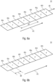
- Fig. 6a shows a schematic representation of a beam deflection device 18, which is formed as an array of facets 46a-h. If the beam deflection device 18 is positioned, for example, in the first position, the facets 46a-d, marked with the numbers 1, 2, 3 and 4, respectively, can deflect beam paths from four optical channels in a first direction. If the beam deflecting device 18 has the second position, the beam path of each optical channel can be deflected in the second direction based on the facets 46e-h, as indicated by the numbers 1', 2', 3' and 4', respectively.
- the facets 46a-d and 46e-h can, for example, be referred to as being arranged in blocks.
- a distance 88 can be covered, which essentially corresponds to an extension length of the number of optical channels along the line extension direction 65.
- this is, for example, an extension of four optical channels along the line extension direction 65.
- the number of beam deflection elements be different by a multiple of the optical channels.
- At least one beam deflecting element can be designed or arranged in a position of the beam deflecting device in order to deflect beam paths from at least two optical channels.
- Fig. 6b shows a schematic view of the beam deflection device 18, in which the facets 46a-g compared to the illustration in Fig. 6a have a different sorting from each other.
- the beam deflector shown has an alternating arrangement of the optical channels 46a-g for each optical channel, as shown by the order 1, 1', 2, 2', 3, 3', 4 and 4'. This allows a distance 88' along which the beam deflector 18 is moved to be switched between the first position and the second position.
- the distance 88' can be compared to the distance 88 Fig. 6a be low.
- the distance 88' may substantially correspond to the distance between two adjacent optical channels of the array 14.
- Two optical channels can, for example, have a distance or a gap from one another that essentially corresponds to at least one dimension of a facet along the direction of movement 65.
- the distance 88' can also be different from this, for example if a beam deflecting element is designed or arranged in a position of the beam deflecting device in order to deflect beam paths from at least two optical channels.
- Fig. 7a shows a schematic side sectional view of a beam deflection element 172, which can be used as one of the beam deflection regions 46 in beam deflection devices described herein.
- the beam deflecting element 172 can be effective for one, a plurality or all of the optical channels 16a-d and can have a polygon-like cross section. Although a triangular cross section is shown, it could be any other polygon. Alternatively or additionally, the cross section can also have at least one curved surface, whereby an at least partially flat design can be advantageous, particularly in the case of reflective surfaces, in order to avoid imaging errors.
- the two main sides 174a and 174b can be inclined to one another at an angle ⁇ .
- the angle ⁇ can have a value between 1° and 89°, preferably has a value between 5° and 60° and particularly preferably a value between 10° and 30°.
- the main sides 174a and 174b are therefore preferably arranged inclined to one another at an angle of at most 60°.
- the beam deflecting element 172 has, for example, a first side 174a, a second side 174b and a third side 174c. At least two sides, such as sides 174a and 174b, are designed to be reflective, so that the beam deflection element 172 is designed to be reflective on both sides.
- the sides 174a and 174b can be main sides of the beam deflection element 172, i.e. sides whose area is larger than the side 174c.
- the beam deflection element 172 can be wedge-shaped and reflective on both sides. Opposite the surface 174c, i.e. between the surfaces 174a and 174b, another surface can be arranged, which, however, is significantly smaller than the surface 174c. In other words, the wedge formed by the surfaces 174a, 174b and 174c does not have an arbitrary point, but is provided with a surface on the pointed side and is therefore blunted.
- Fig. 7b shows a schematic side sectional view of the beam deflection element 172, in which a suspension or a displacement axis 176 of the beam deflection element 172 is described.
- the displacement axis 176 about which the beam deflection element 172 can be rotatably and/or translationally movable in the beam deflection device 18, can be displaced eccentrically with respect to a center of gravity 178 of the cross section.
- the center of gravity can alternatively also be a point that describes half the dimension of the beam deflection element 172 along a thickness direction 182 and along a direction 184 perpendicular thereto.
- the main page 174a may have a surface normal 175a
- the main page 174b may have a surface normal 175b. If a rotational movement about the displacement axis 176 is used to switch between the first position and the second position of the beam deflection device, the rotational movement of the beam deflection device can be carried out in such a way that between the two positions there is an orientation according to which a main side 174a or 174b of the array 14 is completely facing, is avoided, as it is in connection with Fig. 3b is described. This can also be understood to mean that during a change between the first and the second operating state or position due to the rotational movement, the surface normal 175a and the surface normal 175b of the second main page have an in Fig.
- angles ⁇ 1 and ⁇ 2 of at least 10 ° based on a direction towards the image sensor and possibly parallel to a surface normal of the image sensor. In this way it can be avoided that one of the angles is 0° or 180°, which can mean a high or approximately maximum expansion of the beam deflection device along the thickness direction.
- the displacement axis 176 can, for example, remain unchanged along a thickness direction 182 and have any offset in a direction perpendicular thereto. Alternatively, an offset along the thickness direction 182 is also conceivable.
- the displacement can, for example, take place in such a way that when the beam deflection element 172 rotates about the displacement axis 176, a higher adjustment path is obtained than when it rotates about the center of gravity 178.
- the displacement of the displacement axis 176 can thus change the path by which the edge between the sides 174a and 174b during a rotation is increased at the same rotation angle compared to a rotation about the center of gravity 178.
- the beam deflecting element 172 is preferably arranged such that the edge, i.e.
- the pointed side of the wedge-shaped cross section, between the sides 174a and 174b faces the image sensor.
- a different side 174a or 174b can redirect the beam path of the optical channels. It is clear here that the rotation can be carried out in such a way that the space requirement of the beam deflection device along the thickness direction 182 is small, since a movement of the beam deflection element 172 so that a main side is perpendicular to the image sensor is not necessary.
- Page 174c can also be referred to as the side page or the back page.
- Several beam deflection elements can be connected to one another in such a way that a connecting element is arranged on the side 174c, or runs through the cross section of the beam deflection elements, i.e. is arranged inside the beam deflection elements, approximately in the area of the displacement axis 176.
- the holding element can be arranged in this way that it does not exist or only to a small extent, i.e. i.e., at most 50%, at most 30% or at most 10% protrudes beyond the beam deflection element 172 along the direction 182, so that the holding element does not increase or determine the extent of the overall structure along the direction 182.
- the extension in the thickness direction 182 can alternatively be determined by the lenses of the optical channels, i.e. H. these have the dimension that defines the minimum thickness.
- the beam deflecting element 172 can be made of glass, ceramic, glass ceramic, plastic, metal or a combination of these materials and/or other materials.
- the beam deflecting element 172 can be arranged so that the tip, i.e. that is, the edge between the main pages 174a and 174b faces the image sensor.
- the beam deflection elements can be positioned in such a way that they are only on the back or inside the beam deflection elements, i.e. H. the main pages are not obscured.
- a common holding or connecting element may extend over the back 174c.
- the axis of rotation of the beam deflection element 172 can be arranged eccentrically.
- Fig. 7c shows a schematic perspective view of a multi-aperture imaging device 190, which includes an image sensor 12, and a single-row array 14 of optical channels 16a-d arranged next to one another, for example the optics of the optical channel 16d being different from the optics of the optical channels 16a-c, to represent an overall field of view.
- the beam deflection device 18 includes a number of beam deflection elements 172a-d, which can correspond to the number of optical channels. Alternatively, a smaller number of beam deflection elements can be arranged, for example if at least one beam deflection element is used by two optical channels.
- Each beam deflecting element 172a-d can be assigned to an optical channel 16a-d.
- the beam deflecting elements 172a-d can be formed as a plurality of elements 172. Alternatively, at least two, several or all beam deflection elements 172a-d can be formed in one piece with one another.
- Fig. 7d shows a schematic side sectional view of the beam deflection element 172, the cross section of which is formed as a free-form surface. So the side 174c can have a recess 186, which enables a holding element to be attached, the recess 186 also being able to be formed as a protruding element, for example as a tongue of a tongue-and-groove system.
- the cross section also has a fourth side 174d, which has a smaller surface area than the main sides 174a and 174b and connects them to one another.
- Fig. 7e shows a schematic side sectional view of a first beam deflection element 172a and a second beam deflection element 172b lying behind it in the direction of the illustration.
- the recesses 186a and 186b can be arranged so that they are in the
- Fig. 7f shows a schematic perspective view of the beam deflection device 18, which comprises, for example, four beam deflection elements 172a-d, which are connected to a connecting element 188.
- the connecting element can be used to be movable translationally and/or rotationally by an actuator.
- the connecting element 188 can be formed in one piece and extend over an extension direction, such as the y-direction, on or in the beam deflection elements 172a-d.
- the connecting element 188 can also only be connected to at least one side of the beam deflection device 18, for example if the beam deflection elements 172a-d are formed in one piece.
- a connection to an actuator and/or a connection of the beam deflection elements 172a-d can also be made in any other way, for example by gluing, blasting or soldering.
- Fig. 7g shows schematic side sectional views of parts of a multi-aperture imaging device shown one below the other to illustrate different facets of a beam deflection device described herein.
- the facets may be arranged in any multi-aperture imaging device described herein, such as, for example, part of the multi-aperture imaging device 10 Fig. 1a may be or another multi-aperture imaging device, which is configured, for example, to completely image the overall field of view 70a with two partial fields of view 72a and 72b.
- the main sides of the facets 46a and/or 46b can, for example, be arranged inclined to one another at an equal angle ⁇ 1 , while the main sides of the facet 46e can be arranged inclined to one another at a different angle ⁇ 2 .
- the beam deflector may also have additional facets, such as another facet formed similarly to facet 46e, to enable visual field capture of the multi-aperture imaging device 10".
- a rotation of the facets 46a, 46b and 46e about the common axis of rotation 44, for example by rotating the connecting element 188, together with the different angles ⁇ 1 and ⁇ 2 , can enable a different direction deflection through the rotation movement, so that the rotation leads to a change
- An identical or comparable relative position of the partial visual fields and/or total visual fields to one another is maintained between the first and second positions.
- a different positioning of the partial or total facial funds can be achieved through different Angles ⁇ 1 to ⁇ 6 are obtained, which have the main sides of the facets 46a, 46b and 46e in the respective position relative to the associated image sensor area 24a, 24b or 24e or the optics of the optical channels 16a, 16b and 16e.
- the angle ⁇ 2 can be smaller than the angle ⁇ 1 .
- Fig. 7h shows schematic side sectional views of parts of a multi-aperture imaging device shown one below the other, in which the angle ⁇ 2 is larger than the angle ⁇ 1 .
- the main sides of facets of optical channels with different optical properties can be inclined to one another at an equal angle ⁇ , for example if the overall fields of view are recorded alternately and therefore a shared use of a facet of different optical channels is possible
- the illustrate Fig. 7g and Fig. 7h that the facets, which are assigned to optical channels with different optical properties, can have inclined main sides individually or in groups with an angle ⁇ 1 or ⁇ 2 assigned to the optical property.
- Further groups of optical channels or values of optical properties can be implemented in the multi-aperture imaging device, such as a third focal length or a higher number, so that a higher number of different angles ⁇ is also possible.
- Fig. 8 shows a schematic perspective view of an imaging system 60 according to an exemplary embodiment.
- the imaging system 60 includes the multi-aperture imaging device 10.
- the imaging system 60 comprises, alternatively or in addition to the multi-aperture imaging device 10, at least one multi-aperture imaging device 10′, 10", 10′′′, 20, 20′, 30, 40 and/or 50.
- the imaging system 60 includes a flat housing 92.
- the flat housing 92 includes a first extension 94a along a first housing direction a.
- the flat housing 92 further includes a second extension 94b along a second housing direction b and a third extension 94c along a third housing direction c.
- the Housing direction a can be arranged in space parallel to the thickness direction 57.
- the expansion 94a of the flat housing 92 along the housing direction a can be understood as the smallest dimension of the flat housing 92. Compared to the smallest expansion, other expansions 94b and / or 94c can be along other housing directions b or c at least three times the value, at least five times the value or at least seven times the value compared to the Extent 94a along the housing direction a. To put it simply, the extension 94a can be smaller, significantly smaller or possibly an order of magnitude smaller than other extensions 94b and 94c along other housing directions b and c, respectively.
- the flat housing 92 can include one or more apertures 96a-b, through which the beam path 26 and/or 26' can be deflected, for example based on the beam deflection device of the multi-aperture imaging device 10.
- the apertures can be, for example, electrochromic apertures and/or in one Area of the display can be arranged.
- the imaging system 60 can be designed as a portable device.
- the imaging system 60 may be a portable communication device such as a cell phone or so-called smartphone, a tablet computer, or a portable music player.
- the imaging system 60 can be implemented as a monitor, for example for use in a navigation, multimedia or television system.
- the imaging system 60 can also be arranged behind reflective surfaces, such as a mirror.
- an arrangement of a multi-aperture imaging device 10', 10", 10', 20, 20', 30, 40 and/or 50 can be advantageous, since based on the arrangement of the components along the long housing sides 94b and/or 94c Expansion of the multi-aperture imaging device along the housing direction 94a can be small, so that the imaging system 60 can have a small expansion 94a.
- a relative, two-dimensional lateral movement of the image sensor and lens which in conventional systems is a two-dimensional angular change in the field of view (corresponds to a Scanning) can be replaced by a one-dimensional change in the viewing direction and a rotational movement.
- a one-dimensional change in the viewing direction can be done by changing the orientation of the mirror (beam deflecting device) with respect to the optical axis (line extension direction) of the imaging channels by moving the rotatably mounted mirror to another Orientation is brought, whereby the axis of rotation of the mirror can run perpendicular or almost perpendicular to the optical axes of the imaging channels.
- the image sensor and/or array lens array of optical channels
- the components e.g. actuators
- subsystems such as image processing arranged to realize the movement
- the components e.g. actuators
- subsystems such as image processing arranged to realize the movement
- the components e.g. actuators
- subsystems such as image processing arranged to realize the movement
- the components e.g. actuators
- subsystems such as image processing arranged to realize the movement
- This enables spatial separation of movement units (actuators) for optical image stabilization.
- actuators for optical image stabilization.
- a reduction in the number of required components can be achieved and thus the production price of camera systems can be low and a significant reduction in the overall height can be achieved compared to conventional structures.
- a difference to known systems may be that the diameters of the lenses (optics) of the optical channels can essentially define the distance between the planes 52a and 52b. This allows the device to have a low overall height, which is advantageous.
- a principal plane of the lenses is parallel to planes 52a and 52b, whereas the principal plane of the array's optics is arranged orthogonally thereto.
- Fig. 9 shows a schematic perspective view of a device 80, which includes a housing 72 and a first multi-aperture imaging device 10a and a second multi-aperture imaging device 10b arranged in the housing 72.
- the device 80 is designed to record the overall fields of view 70a and 70b at least partially, for example in the overlapping area of the detection areas, stereoscopically with the multi-aperture imaging devices.
- the overall fields of view 70a and 70b are arranged, for example, on a main side 74b of the housing facing away from the main side 74a.
- the multi-aperture imaging devices 10a and 10b can capture the overall field of view 70 through transparent areas 68a and 68c, respectively, with apertures 78a and 78c arranged in the main side 74b being at least partially transparent.
- Apertures 78b and 78d arranged in the main page 74a can at least partially optically close transparent areas 68b and 68d, respectively, so that an amount of false light from a side facing the main page 74a, which can distort the recordings of the multi-aperture imaging devices 10a and / or 10b, is at least reduced is.
- the multi-aperture imaging devices 10a and 10b are shown spatially spaced apart from one another, the multi-aperture imaging devices 10a and 10b may also be spatially adjacent or combined. For example, they can Single-line arrays of the imaging devices 10a and 10b can be arranged next to one another or parallel to one another. The single-row arrays may form rows of one another, with each multi-aperture imaging device 10a and 10b having a single-row array.
- the imaging devices 10a and 10b may have a common beam deflection device, and/or a common carrier 62 and/or a common image sensor 12.
- the multi-aperture imaging device 10′, 10′′, 10′′′, 20, 20′, 30, 40 and/or 50 can be arranged.
- Such common elements such as the beam deflection device or the array, can can be used by a common optical image stabilizer, since, for example, a movement of the beam deflection device for optical channels of several modules can act as optical image stabilization.
- the optical image stabilizer can also be designed together for several modules and / or a common reference channel can be used for several modules .
- the transparent areas 68a-d can additionally be equipped with a switchable shutter 78a-d, which covers the optical structure when not in use.
- the aperture 78a-d may include a mechanically moving part. The movement of the mechanically moved part can take place using an actuator, as described for example for the actuators 36 and 45.
- the aperture 78a-d can alternatively or additionally be electrically controllable and comprise an electrochromic layer or an electrochromic layer sequence, i.e. i.e., be formed as an electrochromic diaphragm.
- Fig. 10 shows a schematic structure comprising a first multi-aperture imaging device 190a and a second multi-aperture imaging device 190b, as can be arranged, for example, in the imaging system 80.
- the arrays 14a and 14b are formed in one row and form a common row.
- the image sensors 12a and 12b can be mounted on a common substrate or on a common circuit carrier, such as a common circuit board or a common flexboard. Alternatively, the image sensors 12a and 12b can also comprise different substrates.
- multi-aperture imaging devices comprising a common image sensor, a common array and/or a common beam deflector 18, as well as other multi-aperture imaging devices that have separate components.
- a common image sensor, a common array and/or a common beam deflection device is that a movement of a respective component also occurs high precision can be obtained by controlling a small number of actuators and synchronization between actuators can be reduced or avoided. Furthermore, high thermal stability can be obtained.
- other and/or different multi-aperture imaging devices 10', 10", 10', 20, 20', 30, 40 and/or 50 can also have a common array, a common image sensor and/or a common beam deflection device.
- FIG. 11a-e A schematic sequence of an electronic image stabilization as it can be provided by the electronic image stabilizer 41 is described. Due to slight differences in the optical properties of the optics of the optical channels, the imaging shifts also differ slightly compared to a difference in the optical properties between the optics 64a-d and 64e. Although the change in imaging caused in the optical channel 64e of the multi-aperture imaging device 10 by movement of the common beam diverter 18 may be larger, the electronic image stabilization in this channel functions similarly. It may be sufficient to carry out the electronic image stabilization in channel 16e independently of the other images. Alternatively, a common reference channel for all optical channels can also be used, since the functional relationships in the multi-aperture imaging device are known.
- Fig. 11a is a schematic representation of an initial situation of an embodiment of electronic image stabilization, such as can be achieved by imaging systems described herein, whereby the statements with regard to electronic image stabilization can also be referred to individual multi-aperture imaging devices without restrictions.
- the imaging system uses a common optical image stabilizer and a common electronic image stabilizer.
- each module has two optical channels 16a and 16b or 16c and 16d in order to image the entire field of view with an object 71.
- the images 73a and 73b of the optical channels 16a and 16b in the associated image sensor areas are referred to as the left image 75a and images 73c and 73d of the optical channels 16c and 16d as the right image of a stereoscopic detection of the object 71.
- Fig. 11a now shows an error-free state in which the object 71 is imaged onto the image sensor areas in order to obtain the images 73a-d.
- the images 73a and 73b can be formed from the multi-aperture imaging device into a left overall image 77a can be combined, for example by stitching.
- the images 73c and 73d can be combined in a comparable manner by the multi-aperture imaging device to form a right overall image 77b, so that stereoscopic information regarding the object 71 can be determined through the two overall images 75a and 75b.
- Fig. 11b now shows the case Fig. 11a , in which a relative movement of the imaging system relative to the object 71 leads to a changed relative position of the object 71 relative to the imaging system, represented by the object 71 '.
- This can be, for example, a movement of the object 71 and/or a shaking of the imaging system. If image corrections are neglected, the relative movement now leads to a changed image position of the image of the object 71 in the image sensor areas, which is shown by the dashed lines of the images 73'ad.
- the aim is now to preserve images 77a and 77b, which are in Fig. 11a are shown, i.e. error-compensated images.
- the aim is to compensate for camera shake, i.e. optimal image stabilization. In this consideration, deviations in the optics of the optical channels are not taken into account.
- Fig. 11c shows the basics for optical image stabilization in the images under the unchanged assumption that pure optical image stabilization of all optimal optical channels, which have identical optical parameters, i.e. have an identical focal length, leads to optimal image stabilization.
- the displacement of the object 71 is represented by an arrow 79 which points in the positive direction 28 and negative direction 32.
- 11c be done as quickly as possible in order to prevent the offset shown from occurring in the first place.
- the directions represented by arrows 84a-d and 77a-b are arranged in space opposite to arrow 79, for example at prominent points in the respective partial image, such as an eye or the corner of the mouth, which means, for example, edges in the image.
- Fig. 11d The partial images 73"ad obtained after the optical image stabilization and taking into account the actual deviations in the optical properties are now shown.
- the optical image stabilization is carried out, for example, in such a way that the image 73a is optimally corrected, which means that the optically image-stabilized image 73"a corresponds to the error-free image 73a, at least within a tolerance range that indicates the possibilities of the optical image stabilizer.
- the image stabilization in the optical channel 16a now has a different effect in the channels 16b-d, which means that the deviations in the optical properties cause, for example, that the arrows 82a-d, which indicate the displacement of the Images based on optical stabilization may vary in length and/or direction.
- Fig. 11e shows in the images of the channels 16b-c the optical image stabilization now carried out compared to the reference channel 16a, which is indicated by the images 73" ⁇ bd.
- Electronic image stabilization in the channels 16b-d away from the channel 16a reduces their deviations from the optical image stabilization in the optical channel 16a at least partially compensated, so that error-reduced or even error-free images 77" ⁇ a and 77" ⁇ b can be obtained, which can correspond to the images 77a and 77b.
- This means that partially compensated image positions are compensated by optical image stabilization and Image layers obtained through additional electronic image stabilization.
- the extent of the electronic image stabilization can be carried out by the electronic image stabilizer using the functional relationship between the optical channels 16a-d.
- the electronic image stabilizer such as the image stabilizer 41, can be designed to the extent the shift in the images, for example by looking at a matching feature in two temporally different or consecutive frames.
- the reference channel can also be the optical channel 16e.
- Fig. 12 shows a schematic flowchart of a method 1200 for providing a multi-aperture imaging device according to an exemplary embodiment.
- an image sensor is provided.
- an array of optical channels is provided so that each optical channel includes optics for imaging at least a partial field of view of a total field of view onto an image sensor area of the image sensor and so that a first optical channel of the array is designed to form a first partial field of view to image the first overall field of view, so that a second optical channel of the array is designed to image a second partial field of view of the first overall field of view, and so that a third optical channel is designed to completely image a second overall field of view and so that the second overall field of view is an incomplete section of the first overall field of view.
- a beam deflecting device is arranged to deflect a beam path of the optical channels.
- Fig. 13 shows a schematic flow diagram of a method 1300 for providing a multi-aperture imaging device according to an exemplary embodiment, for example the multi-aperture imaging device 10".
- an image sensor is provided.
- an array of optical channels is provided, so that each optical channel has one Optics for imaging at least a partial field of view of a total field of view on an image sensor area of the image sensor, so that a first optical channel of the array is designed to image a first partial field of view of a first total field of view, so that a second optical channel of the array is designed to a second partial field of view of the first overall field of view, and so that a third optical channel is designed to completely image a second overall field of view, and so that the second overall field of view is an incomplete section of the first overall field of view.
- a beam deflecting device is arranged to deflect a beam path of the optical channels.
- Fig. 14 shows a schematic flowchart of a method 1400 for providing a further multi-aperture imaging device according to a further exemplary embodiment.
- a step 1410 an image sensor is provided.
- an array comprising at least a first and a second optical channel is provided, so that each optical channel comprises optics for imaging an overall field of view onto an image sensor area of the image sensor and so that the optics of the first optical channel have a focal length, by at least 10% is different from a focal length of the optics of the second optical channel.
- a beam deflecting device is arranged to jointly deflect a beam path of the optical channels.
- the explanations made in connection with the electronic image stabilizer or a combination of the optical image stabilizer with the electronic image stabilizer and presented for the multi-aperture imaging device 10 also apply to the other multi-aperture imaging devices described herein, in particular the multi-aperture imaging device 10 "and 10".
- the different Optical properties of the optics in interaction with the common beam deflection device and the common array can be compensated for via a channel-specific electronic image stabilization, if necessary by determining a reference channel that is linked to the at least one other optical channel.
- a possibly arranged optical image stabilizer can be designed, in order to achieve optimal or highest possible optical stabilization for one channel, so that electronic stabilization is carried out in the remaining channels.
- the optical image stabilizer may be designed to reduce overall image error across all images and the electronic image stabilizer may be designed to perform electronic stabilization in all channels.
- the optical image stabilizer can be designed to carry out the optical image stabilization in such a way that the optical image stabilization is based on a reference image of one of the first and second overall fields of view.
- the electronic image stabilizer is designed to stabilize an image of a different overall field of view based on the reference image.
- the multi-aperture imaging device can also be designed here to exclusively optically stabilize the reference image.
- the electronic image stabilizer can further be designed to carry out the channel-specific electronic image stabilization in each channel according to a defined functional relationship, which depends on the relative movements between the image sensor, the array and the beam deflecting device, as described above in connection with Fig. 5b is described.
- Embodiments described herein enable multi-aperture imaging systems with a linear channel arrangement, ie single-line or multi-line along a line extension direction, with optical image stabilization using uniaxial translational movement between the image sensor and imaging optics as well as uniaxial rotational movement of a beam-deflecting mirror array.
- multi-aperture imaging devices may include any number of optical channels, for example at least two, at least three, at least four, at least ten or one higher number of optical channels can be arranged.
- the actuators 36 and 42 can also be designed as a common actuator.
- a movement generated by the actuator can be guided to the image sensor 12, the optical array 14 and/or the beam deflection device 18 by means of a force and/or displacement converter (gear) in order to obtain a respective movement.
- a force and/or displacement converter gear
- one or more components can also be moved by several actuators, as described, for example, in connection with the multi-aperture imaging device 50.
- the image sensor can, for example, be designed as a complementary metal-oxide-semiconductor (CMOS) or a different technology.
- CMOS complementary metal-oxide-semiconductor
- the optical channels of a respective array can be understood as defining an area in which a beam path that is guided onto a respective image sensor area is optically changed. A beam path assigned to an image sensor area can thus travel through the optical channel of the array.
- the beam paths or optical axes can be directed in different directions from the beam deflection device. This can be achieved by directing the beam paths during a deflection at the beam deflection device and/or through the optics other than parallelism to one another.
- the beam paths or optical axes can deviate from parallelism before or without beam deflection.
- the channels can be provided with a kind of advance divergence. With this advance divergence of the optical axes, it would be possible, for example, for not all facet inclinations of facets of the beam deflection device to differ from one another, but for some groups of channels, for example, to have facets with the same inclination or directed towards them.
- the latter can then be formed in one piece or continuously merging into one another, so to speak as a facet that is assigned to this group of channels adjacent in the direction of the line extension.
- the divergence of the optical axes of these channels could then come from the divergence of these optical axes, as achieved by a lateral offset between optical centers of the optics of the optical channels and image sensor areas of the channels.
- the preliminary divergence could, for example, be limited to one level.
- the optical axes could, for example, run in a common plane before or without beam deflection, but divergent in this, and the facets only cause an additional divergence in the other transversal plane, that is, they are all parallel to the line extension direction and only different from one another than the one mentioned above common plane of the optical axes inclined, whereby here again several facets can have the same inclination or could be assigned to a group of channels, the optical axes of which, for example, already differ in the aforementioned common plane of the optical axes in pairs before or without beam deflection.
- the optics can enable a (preliminary) divergence of the beam paths along a first (image) direction and the beam deflection device can enable a divergence of the beam paths along a second (image) direction.
- the previously mentioned possibly existing divergence can be achieved, for example, by the optical centers of the optics lying on a straight line along the line extension direction, while the centers of the image sensor areas depend on the projection of the optical centers along the normal of the plane of the image sensor areas onto points on a straight line the image sensor plane are arranged differently, such as at points that deviate from the points on the aforementioned straight line in the image sensor plane on a channel-specific basis along the line extension direction and/or along the direction perpendicular to both the line extension direction and the image sensor normal.
- advance divergence can be achieved by having the centers of the image sensors lie on a straight line along the line extension direction, while the centers of the optics depend on the projection of the optical centers of the image sensors along the normal of the plane of the optical centers of the optics to points on a straight line the optical center plane are arranged differently, such as at points that deviate from the points on the aforementioned straight line in the optical center plane on a channel-specific basis along the line extension direction and/or along the direction perpendicular to both the line extension direction and the normal of the optical center plane. It is preferred if the aforementioned channel-specific deviation from the respective projection only runs in the line extension direction, i.e. the optical axes are only in a common plane with a preliminary divergence.
- optical centers and image sensor area centers then lie on a straight line parallel to the line extension direction, but with different spacings.
- a lateral offset between lenses and image sensors in a perpendicular lateral direction to the line extension direction led to an increase in the overall height.
- a pure in-plane offset in the line extension direction does not change the overall height, but this may result in fewer facets and/or the facets only have a tilt in one angular orientation, which simplifies the structure.
- adjacent optical channels can have optical axes that run in the common plane and are mutually squinting, i.e. provided with a pre-divergence.
- a facet can be arranged with respect to a group of optical channels, inclined in only one direction and parallel to the line extension direction.
- optical channels are assigned to the same partial field of view, for example for the purpose of superresolution or to increase the resolution with which the corresponding partial field of view is scanned by these channels.
- the optical channels within such a group would then run parallel, for example, before the beam was deflected and would be redirected to a partial field of view by a facet.
- pixel images of the image sensor of a channel of a group would lie in intermediate positions between images of the pixels of the image sensor of another channel of this group.
- the above exemplary embodiments can therefore be implemented in the form of a multi-aperture imaging device and/or an imaging system comprising such a multi-aperture imaging device, with a single-line channel arrangement, whereby each channel transmits a partial field of view of an overall field of view and the partial fields of view partially overlap.
- a setup with several such multi-aperture imaging devices for stereo, trio, quattro, etc. setups for 3D image recording is possible.
- the majority of modules can be executed as a continuous line be.
- the connected row could use identical actuators and a common beam deflecting element.
- One or more reinforcing substrates that may be present in the beam path can extend over the entire line, which can form a stereo, trio, quattro structure.
- Superresolution methods can be used, with several channels imaging the same partial image areas.
- the optical axes can also run divergently without a beam deflection device, so that fewer facets are required on the beam deflection unit.
- the facets then advantageously only have one angular component.
- the image sensor can be in one piece, have only one connected pixel matrix or several interrupted ones.
- the image sensor can be composed of many sub-sensors, which are arranged next to one another on a circuit board, for example.
- An autofocus drive can be designed so that the beam deflecting element is moved synchronously with the optics or is stationary.
- aspects have been described in connection with a device, it is understood that these aspects also represent a description of the corresponding method, so that a block or a component of a device is also to be understood as a corresponding method step or as a feature of a method step. Analogously, aspects that have been described in connection with or as a method step also represent a description of a corresponding block or detail or feature of a corresponding device.
Landscapes
- Physics & Mathematics (AREA)
- Engineering & Computer Science (AREA)
- Multimedia (AREA)
- Signal Processing (AREA)
- General Physics & Mathematics (AREA)
- Optics & Photonics (AREA)
- Human Computer Interaction (AREA)
- Studio Devices (AREA)
- Adjustment Of Camera Lenses (AREA)
- Cameras In General (AREA)
- Stereoscopic And Panoramic Photography (AREA)
- Structure And Mechanism Of Cameras (AREA)
- Lenses (AREA)
- Photometry And Measurement Of Optical Pulse Characteristics (AREA)
Applications Claiming Priority (4)
| Application Number | Priority Date | Filing Date | Title |
|---|---|---|---|
| DE102017206429.3A DE102017206429A1 (de) | 2017-04-13 | 2017-04-13 | Multiaperturabbildungsvorrichtung, Abbildungssystem und Verfahren zum Bereitstellen einer Multiaperturabbildungsvorrichtung |
| EP21163222.9A EP3860108B1 (fr) | 2017-04-13 | 2018-04-12 | Dispositif de reproduction multi-ouverture, système de reproduction et procédé de fourniture d'un dispositif de reproduction multi-ouverture |
| EP18721962.1A EP3610636B1 (fr) | 2017-04-13 | 2018-04-12 | Dispositif de reproduction multi-ouverture, système de reproduction et procédé de fourniture d'un dispositif de reproduction multi-ouverture |
| PCT/EP2018/059443 WO2018189321A1 (fr) | 2017-04-13 | 2018-04-12 | Dispositif de reproduction multi-ouverture, système de reproduction et procédé de fourniture d'un dispositif de reproduction multi-ouverture |
Related Parent Applications (3)
| Application Number | Title | Priority Date | Filing Date |
|---|---|---|---|
| EP21163222.9A Division-Into EP3860108B1 (fr) | 2017-04-13 | 2018-04-12 | Dispositif de reproduction multi-ouverture, système de reproduction et procédé de fourniture d'un dispositif de reproduction multi-ouverture |
| EP21163222.9A Division EP3860108B1 (fr) | 2017-04-13 | 2018-04-12 | Dispositif de reproduction multi-ouverture, système de reproduction et procédé de fourniture d'un dispositif de reproduction multi-ouverture |
| EP18721962.1A Division EP3610636B1 (fr) | 2017-04-13 | 2018-04-12 | Dispositif de reproduction multi-ouverture, système de reproduction et procédé de fourniture d'un dispositif de reproduction multi-ouverture |
Publications (3)
| Publication Number | Publication Date |
|---|---|
| EP4242719A2 true EP4242719A2 (fr) | 2023-09-13 |
| EP4242719A3 EP4242719A3 (fr) | 2023-10-18 |
| EP4242719B1 EP4242719B1 (fr) | 2025-01-01 |
Family
ID=62111019
Family Applications (3)
| Application Number | Title | Priority Date | Filing Date |
|---|---|---|---|
| EP18721962.1A Active EP3610636B1 (fr) | 2017-04-13 | 2018-04-12 | Dispositif de reproduction multi-ouverture, système de reproduction et procédé de fourniture d'un dispositif de reproduction multi-ouverture |
| EP21163222.9A Active EP3860108B1 (fr) | 2017-04-13 | 2018-04-12 | Dispositif de reproduction multi-ouverture, système de reproduction et procédé de fourniture d'un dispositif de reproduction multi-ouverture |
| EP23173334.6A Active EP4242719B1 (fr) | 2017-04-13 | 2018-04-12 | Dispositif de reproduction multi-ouverture, système de reproduction et procédé de fourniture d'un dispositif de reproduction multi-ouverture |
Family Applications Before (2)
| Application Number | Title | Priority Date | Filing Date |
|---|---|---|---|
| EP18721962.1A Active EP3610636B1 (fr) | 2017-04-13 | 2018-04-12 | Dispositif de reproduction multi-ouverture, système de reproduction et procédé de fourniture d'un dispositif de reproduction multi-ouverture |
| EP21163222.9A Active EP3860108B1 (fr) | 2017-04-13 | 2018-04-12 | Dispositif de reproduction multi-ouverture, système de reproduction et procédé de fourniture d'un dispositif de reproduction multi-ouverture |
Country Status (9)
| Country | Link |
|---|---|
| US (1) | US10996460B2 (fr) |
| EP (3) | EP3610636B1 (fr) |
| JP (1) | JP7019720B2 (fr) |
| KR (1) | KR102303135B1 (fr) |
| CN (1) | CN110771135B (fr) |
| DE (1) | DE102017206429A1 (fr) |
| ES (1) | ES2887034T3 (fr) |
| TW (1) | TWI686623B (fr) |
| WO (1) | WO2018189321A1 (fr) |
Families Citing this family (9)
| Publication number | Priority date | Publication date | Assignee | Title |
|---|---|---|---|---|
| US11448886B2 (en) | 2018-09-28 | 2022-09-20 | Apple Inc. | Camera system |
| US11187914B2 (en) * | 2018-09-28 | 2021-11-30 | Apple Inc. | Mirror-based scene cameras |
| DE102019204075B4 (de) * | 2019-03-25 | 2022-03-31 | Fraunhofer-Gesellschaft zur Förderung der angewandten Forschung e.V. | Vorrichtung mit einer Multiaperturabbildungsvorrichtung zur Erzeugung einer Tiefenkarte |
| CN114270815B (zh) * | 2019-06-06 | 2025-03-18 | 弗劳恩霍夫应用研究促进协会 | 多通道成像设备和具有多孔径成像设备的设备 |
| CN112394536B (zh) * | 2019-07-31 | 2022-04-29 | 华为技术有限公司 | 一种光学防抖装置及控制方法 |
| WO2021035090A1 (fr) * | 2019-08-21 | 2021-02-25 | Arizona Board Of Regents On Behalf Of The University Of Arizona | Système d'imagerie à polarisation reconfigurable |
| US11107678B2 (en) * | 2019-11-26 | 2021-08-31 | Canon Kabushiki Kaisha | Wafer process, apparatus and method of manufacturing an article |
| EP4602833A1 (fr) * | 2022-10-10 | 2025-08-20 | Urugus S.A. | Système et procédé de stabilisation pour scènes d'imagerie à mouvement apparent |
| CN120223185B (zh) * | 2023-12-26 | 2026-04-07 | 重庆鸿图智光光电科技合伙企业(普通合伙) | 一种光学和电学综合合成的空间光通信多孔径接收方法 |
Family Cites Families (65)
| Publication number | Priority date | Publication date | Assignee | Title |
|---|---|---|---|---|
| JP4411059B2 (ja) * | 2003-12-12 | 2010-02-10 | キヤノン株式会社 | カメラ付きディスプレイ装置、通信装置および通信システム |
| JP5934459B2 (ja) | 2006-04-17 | 2016-06-15 | オムニビジョン テクノロジーズ, インコーポレイテッド | アレイ化撮像システムおよび関連方法 |
| JP2008026712A (ja) * | 2006-07-24 | 2008-02-07 | Eastman Kodak Co | 複数光学系を有する撮像装置 |
| US20080030592A1 (en) | 2006-08-01 | 2008-02-07 | Eastman Kodak Company | Producing digital image with different resolution portions |
| KR100871566B1 (ko) * | 2006-12-04 | 2008-12-02 | 삼성전자주식회사 | 이미지 촬상 장치의 손떨림 보상을 위한 장치 및 방법 |
| US7643063B2 (en) | 2006-12-29 | 2010-01-05 | The Boeing Company | Dual loop stabilization of video camera images |
| US20090122195A1 (en) | 2007-11-09 | 2009-05-14 | Van Baar Jeroen | System and Method for Combining Image Sequences |
| CN102356630B (zh) | 2009-03-19 | 2016-01-27 | 数字光学公司 | 双传感器照相机 |
| AU2009201637B2 (en) | 2009-04-24 | 2011-08-11 | Canon Kabushiki Kaisha | Processing multi-view digital images |
| US9144714B2 (en) | 2009-05-02 | 2015-09-29 | Steven J. Hollinger | Ball with camera for reconnaissance or recreation and network for operating the same |
| US20100328471A1 (en) * | 2009-06-24 | 2010-12-30 | Justin Boland | Wearable Multi-Channel Camera |
| US20110026141A1 (en) * | 2009-07-29 | 2011-02-03 | Geoffrey Louis Barrows | Low Profile Camera and Vision Sensor |
| US9036102B2 (en) * | 2009-12-23 | 2015-05-19 | Lensvector Inc. | Image stabilization and shifting in a liquid crystal lens |
| JP5553597B2 (ja) | 2009-12-25 | 2014-07-16 | キヤノン株式会社 | 撮像装置及びその制御方法 |
| JP5506504B2 (ja) | 2010-03-31 | 2014-05-28 | キヤノン株式会社 | 撮像装置及び撮像方法 |
| JP2012037749A (ja) | 2010-08-09 | 2012-02-23 | Ricoh Co Ltd | 電子写真感光体の製造方法、電子写真感光体、及び画像形成装置 |
| US20120075489A1 (en) * | 2010-09-24 | 2012-03-29 | Nishihara H Keith | Zoom camera image blending technique |
| US20120098971A1 (en) * | 2010-10-22 | 2012-04-26 | Flir Systems, Inc. | Infrared binocular system with dual diopter adjustment |
| JP5830662B2 (ja) | 2010-12-09 | 2015-12-09 | パナソニックIpマネジメント株式会社 | 撮像装置 |
| US10412367B2 (en) * | 2011-08-05 | 2019-09-10 | 3D Media Ltd | Multi-lens camera with a single image sensor |
| JP2013045032A (ja) | 2011-08-26 | 2013-03-04 | Fujifilm Corp | 多眼撮像装置 |
| EP2582128A3 (fr) * | 2011-10-12 | 2013-06-19 | Canon Kabushiki Kaisha | Dispositif de capture d'image |
| US9395516B2 (en) * | 2012-05-28 | 2016-07-19 | Nikon Corporation | Imaging device |
| JP6004785B2 (ja) * | 2012-06-29 | 2016-10-12 | キヤノン株式会社 | 撮像装置、光学機器、撮像システムおよび制御方法 |
| US20140002674A1 (en) * | 2012-06-30 | 2014-01-02 | Pelican Imaging Corporation | Systems and Methods for Manufacturing Camera Modules Using Active Alignment of Lens Stack Arrays and Sensors |
| US9398264B2 (en) * | 2012-10-19 | 2016-07-19 | Qualcomm Incorporated | Multi-camera system using folded optics |
| EP2918076A4 (fr) | 2012-11-12 | 2016-10-05 | Behavioral Recognition Sys Inc | Techniques de stabilisation d'image destinées à des systèmes de surveillance vidéo |
| CN113259565B (zh) | 2012-11-28 | 2023-05-19 | 核心光电有限公司 | 多孔径成像系统 |
| JP6172161B2 (ja) | 2012-12-11 | 2017-08-02 | コニカミノルタ株式会社 | 複眼光学系とそれを用いた撮像装置 |
| US20140160231A1 (en) | 2012-12-12 | 2014-06-12 | Daniel C. Middleton | Multi-focal image capture and display |
| DE102013208625A1 (de) * | 2013-05-10 | 2014-11-13 | Fraunhofer-Gesellschaft zur Förderung der angewandten Forschung e.V. | Multiapertur-projektionsdisplay und einzelbilderzeuger für ein solches |
| JP6100089B2 (ja) | 2013-05-17 | 2017-03-22 | キヤノン株式会社 | 画像処理装置、画像処理方法およびプログラム |
| US9232138B1 (en) | 2013-06-03 | 2016-01-05 | Amazon Technologies, Inc. | Image stabilization techniques |
| JP6429440B2 (ja) | 2013-09-18 | 2018-11-28 | キヤノン株式会社 | 撮像装置、その制御方法、および制御プログラム |
| CN105830425A (zh) * | 2013-10-18 | 2016-08-03 | 泽莱特科股份有限公司 | 用于捕获和/或组合图像的方法和装置 |
| US9549127B2 (en) * | 2013-10-18 | 2017-01-17 | Light Labs Inc. | Image capture control methods and apparatus |
| US9423588B2 (en) * | 2013-10-18 | 2016-08-23 | The Lightco Inc. | Methods and apparatus for supporting zoom operations |
| DE102013222780B3 (de) * | 2013-11-08 | 2015-04-16 | Fraunhofer-Gesellschaft zur Förderung der angewandten Forschung e.V. | Multiaperturvorrichtung und verfahren zur erfassung eines objektbereichs |
| KR102163045B1 (ko) * | 2014-02-17 | 2020-10-08 | 삼성전기주식회사 | 이미지 보정 장치 및 그 방법 |
| JP2015185947A (ja) | 2014-03-20 | 2015-10-22 | 株式会社東芝 | 撮像システム |
| US9383550B2 (en) * | 2014-04-04 | 2016-07-05 | Qualcomm Incorporated | Auto-focus in low-profile folded optics multi-camera system |
| DE102014213371B3 (de) * | 2014-07-09 | 2015-08-06 | Fraunhofer-Gesellschaft zur Förderung der angewandten Forschung e.V. | Vorrichtung und verfahren zur erfassung eines objektbereichs |
| US9596411B2 (en) | 2014-08-25 | 2017-03-14 | Apple Inc. | Combined optical and electronic image stabilization |
| US20160173869A1 (en) | 2014-12-15 | 2016-06-16 | Nokia Corporation | Multi-Camera System Consisting Of Variably Calibrated Cameras |
| JP6436783B2 (ja) | 2015-01-09 | 2018-12-12 | キヤノン株式会社 | 画像処理装置、撮像装置、画像処理方法、プログラム、および、記憶媒体 |
| KR102088603B1 (ko) * | 2015-04-16 | 2020-03-13 | 코어포토닉스 리미티드 | 소형 접이식 카메라의 오토 포커스 및 광학 이미지 안정화 |
| DE102015215837A1 (de) | 2015-08-19 | 2017-02-23 | Fraunhofer-Gesellschaft zur Förderung der angewandten Forschung e.V. | Multiaperturabbildungsvorrichtung, Verfahren zum Herstellen derselben und Abbildungssystem |
| DE102015215833A1 (de) | 2015-08-19 | 2017-02-23 | Fraunhofer-Gesellschaft zur Förderung der angewandten Forschung e.V. | Multiaperturabbildungsvorrichtung mit Optiksubstrat |
| DE102015215841B4 (de) | 2015-08-19 | 2017-06-01 | Fraunhofer-Gesellschaft zur Förderung der angewandten Forschung e.V. | Vorrichtung mit einer Multikanalabbildungsvorrichtung und Verfahren zum Herstellen derselben |
| DE102015215844B4 (de) * | 2015-08-19 | 2017-05-18 | Fraunhofer-Gesellschaft zur Förderung der angewandten Forschung e.V. | Multiaperturabbildungsvorrichtung, tragbare Vorrichtung und Verfahren zum Herstellen einer Multiaperturabbildungsvorrichtung |
| DE102015215840B4 (de) | 2015-08-19 | 2017-03-23 | Fraunhofer-Gesellschaft zur Förderung der angewandten Forschung e.V. | Multiaperturabbildungsvorrichtung, Abbildungssystem und Verfahren zum Bereitstellen einer Multiaperturabbildungsvorrichtung |
| DE102015215836B4 (de) | 2015-08-19 | 2017-05-18 | Fraunhofer-Gesellschaft zur Förderung der angewandten Forschung e.V. | Multiaperturabbildungsvorrichtung mit einer reflektierende Facetten aufweisenden Strahlumlenkvorrichtung |
| DE102015215845B4 (de) * | 2015-08-19 | 2017-06-22 | Fraunhofer-Gesellschaft zur Förderung der angewandten Forschung e.V. | Multiaperturabbildungsvorrichtung mit kanalindividueller Einstellbarkeit |
| DE102015216140A1 (de) | 2015-08-24 | 2017-03-02 | Fraunhofer-Gesellschaft zur Förderung der angewandten Forschung e.V. | 3D-Multiaperturabbildungsvorrichtung |
| ITUB20154043A1 (it) | 2015-09-30 | 2017-03-30 | Datalogic IP Tech Srl | Sistema e metodo di lettura di informazioni codificate |
| DE102015220566B4 (de) | 2015-10-21 | 2021-03-18 | Fraunhofer-Gesellschaft zur Förderung der angewandten Forschung e.V. | Vorrichtung mit einer Multiaperturabbildungsvorrichtung, Verfahren zum Bereitstellen derselben und Verfahren zum Erfassen eines Gesamtgesichtsfeldes |
| DE102016200287A1 (de) | 2016-01-13 | 2017-07-13 | Fraunhofer-Gesellschaft zur Förderung der angewandten Forschung e.V. | Multiaperturabbildungsvorrichtungen, Verfahren zum Herstellen derselben und Abbildungssystem |
| DE102016200285A1 (de) | 2016-01-13 | 2017-07-13 | Fraunhofer-Gesellschaft zur Förderung der angewandten Forschung e.V. | Multiaperturabbildungsvorrichtung, Abbildungssystem und Verfahren zum Erfassen eines Objektbereichs |
| DE102016204148A1 (de) | 2016-03-14 | 2017-09-14 | Fraunhofer-Gesellschaft zur Förderung der angewandten Forschung e.V. | Multiaperturabbildungsvorrichtung, Abbildungssystem und Verfahren zum Erfassen eines Objektbereichs |
| DE102016208210A1 (de) | 2016-05-12 | 2017-11-16 | Fraunhofer-Gesellschaft zur Förderung der angewandten Forschung e.V. | 3d-multiaperturabbildungsvorrichtungen, multiaperturabbildungsvorrichtung, verfahren zum bereitstellen eines ausgangssignals einer 3d-multiaperturabbildungsvorrichtung und verfahren zum erfassen eines gesamtgesichtsfeldes |
| US10291866B2 (en) * | 2016-06-24 | 2019-05-14 | Moondog Optics, Inc. | Lens attachment for multi-camera device |
| CN106791377B (zh) * | 2016-11-29 | 2019-09-27 | Oppo广东移动通信有限公司 | 控制方法、控制装置及电子装置 |
| CN106444056B (zh) * | 2016-12-09 | 2020-11-17 | 中国科学院光电技术研究所 | 一种基于三孔径的稀疏光学合成孔径成像装置及其光束合束校正方法 |
| KR102354134B1 (ko) * | 2017-02-23 | 2022-01-21 | 코어포토닉스 리미티드 | 폴디드 카메라 렌즈 설계 |
| CN114137791A (zh) * | 2017-03-15 | 2022-03-04 | 核心光电有限公司 | 具有全景扫瞄范围的照相装置及移动装置 |
-
2017
- 2017-04-13 DE DE102017206429.3A patent/DE102017206429A1/de not_active Withdrawn
-
2018
- 2018-03-30 TW TW107111385A patent/TWI686623B/zh active
- 2018-04-12 EP EP18721962.1A patent/EP3610636B1/fr active Active
- 2018-04-12 EP EP21163222.9A patent/EP3860108B1/fr active Active
- 2018-04-12 KR KR1020197033500A patent/KR102303135B1/ko active Active
- 2018-04-12 CN CN201880039637.8A patent/CN110771135B/zh active Active
- 2018-04-12 EP EP23173334.6A patent/EP4242719B1/fr active Active
- 2018-04-12 JP JP2019555943A patent/JP7019720B2/ja active Active
- 2018-04-12 ES ES18721962T patent/ES2887034T3/es active Active
- 2018-04-12 WO PCT/EP2018/059443 patent/WO2018189321A1/fr not_active Ceased
-
2019
- 2019-10-02 US US16/590,935 patent/US10996460B2/en active Active
Also Published As
| Publication number | Publication date |
|---|---|
| EP3610636B1 (fr) | 2021-05-26 |
| EP3860108B1 (fr) | 2023-06-21 |
| ES2887034T3 (es) | 2021-12-21 |
| EP3610636A1 (fr) | 2020-02-19 |
| JP2020516954A (ja) | 2020-06-11 |
| DE102017206429A1 (de) | 2018-10-18 |
| US10996460B2 (en) | 2021-05-04 |
| CN110771135A (zh) | 2020-02-07 |
| TWI686623B (zh) | 2020-03-01 |
| KR20190138310A (ko) | 2019-12-12 |
| KR102303135B1 (ko) | 2021-09-23 |
| TW201839455A (zh) | 2018-11-01 |
| US20200033588A1 (en) | 2020-01-30 |
| CN110771135B (zh) | 2022-06-07 |
| EP4242719B1 (fr) | 2025-01-01 |
| WO2018189321A1 (fr) | 2018-10-18 |
| EP4242719A3 (fr) | 2023-10-18 |
| JP7019720B2 (ja) | 2022-02-15 |
| EP3860108A1 (fr) | 2021-08-04 |
Similar Documents
| Publication | Publication Date | Title |
|---|---|---|
| EP4242719B1 (fr) | Dispositif de reproduction multi-ouverture, système de reproduction et procédé de fourniture d'un dispositif de reproduction multi-ouverture | |
| EP3225021B1 (fr) | Dispositif de reproduction multiouverture, système de reproduction et procédé de fourniture d'un dispositif de reproduction multiouverture | |
| EP3593201B1 (fr) | Dispositif de reproduction multiouverture, système de reproduction et procédé de fourniture d'un dispositif de reproduction multi-ouverture | |
| EP3403392B1 (fr) | Détecteur optique à ouvertures multiples et methode de détection de signaux optiques | |
| EP3371650B1 (fr) | Dispositif imageur multi-ouvertures, système imageur et procédé de détection d'une zone d'objet | |
| EP3338133B1 (fr) | Dispositif comprenant un dispositif de reproduction à multiples canaux et son procédé de fabrication | |
| EP3366032B1 (fr) | Dispositif comportant un dispositif de reproduction à ouvertures multiples, procédé de fabrication de celui-ci et procédé de détection d'un champ visuel global | |
| DE102015215845B4 (de) | Multiaperturabbildungsvorrichtung mit kanalindividueller Einstellbarkeit | |
| DE102015215836B4 (de) | Multiaperturabbildungsvorrichtung mit einer reflektierende Facetten aufweisenden Strahlumlenkvorrichtung | |
| EP3632094B1 (fr) | Dispositif de reproduction multi-ouverture, système de reproduction et procédé de fourniture d'un dispositif de reproduction multi-ouverture | |
| EP3682626B1 (fr) | Dispositif d'imagerie à ouvertures multiples ayant un faible encombrement en hauteur et une direction d'observation commutable, système d'imagerie et procédé de fabrication d'un dispositif d'imagerie à ouvertures multiples | |
| EP3981145B1 (fr) | Dispositif de reproduction multi-canaux et appareil comportant un dispositif de reproduction multi-ouvertures | |
| DE102017012197B4 (de) | Multiaperturabbildungsvorrichtung, Abbildungssystem und Verfahren zum Bereitstellen einer Multiaperturabbildungsvorrichtung | |
| DE102017211586A1 (de) | Multiaperturabbildungsvorrichtung mit geringer falschlichtempfindlichkeit, abbildungssystem und verfahren zum bereitstellen einer multiaperturabbildungsvorrichtung | |
| WO2020120230A1 (fr) | Dispositif de reproduction multi-canaux et appareil comportant un dispositif de reproduction multi-ouvertures | |
| DE102015017384B4 (de) | Vorrichtung mit einer Multiaperturabbildungsvorrichtung, Verfahren zum Bereitstellen derselben und Verfahren zum Erfassen eines Gesamtgesichtsfeldes |
Legal Events
| Date | Code | Title | Description |
|---|---|---|---|
| PUAI | Public reference made under article 153(3) epc to a published international application that has entered the european phase |
Free format text: ORIGINAL CODE: 0009012 |
|
| STAA | Information on the status of an ep patent application or granted ep patent |
Free format text: STATUS: THE APPLICATION HAS BEEN PUBLISHED |
|
| AC | Divisional application: reference to earlier application |
Ref document number: 3610636 Country of ref document: EP Kind code of ref document: P Ref document number: 3860108 Country of ref document: EP Kind code of ref document: P |
|
| AK | Designated contracting states |
Kind code of ref document: A2 Designated state(s): AL AT BE BG CH CY CZ DE DK EE ES FI FR GB GR HR HU IE IS IT LI LT LU LV MC MK MT NL NO PL PT RO RS SE SI SK SM TR |
|
| PUAL | Search report despatched |
Free format text: ORIGINAL CODE: 0009013 |
|
| AK | Designated contracting states |
Kind code of ref document: A3 Designated state(s): AL AT BE BG CH CY CZ DE DK EE ES FI FR GB GR HR HU IE IS IT LI LT LU LV MC MK MT NL NO PL PT RO RS SE SI SK SM TR |
|
| RIC1 | Information provided on ipc code assigned before grant |
Ipc: H04N 23/698 20230101ALI20230908BHEP Ipc: H04N 23/68 20230101ALI20230908BHEP Ipc: H04N 23/55 20230101ALI20230908BHEP Ipc: H04N 23/54 20230101ALI20230908BHEP Ipc: H04N 23/45 20230101ALI20230908BHEP Ipc: G02B 27/64 20060101ALI20230908BHEP Ipc: G02B 26/08 20060101ALI20230908BHEP Ipc: G02B 13/00 20060101AFI20230908BHEP |
|
| STAA | Information on the status of an ep patent application or granted ep patent |
Free format text: STATUS: REQUEST FOR EXAMINATION WAS MADE |
|
| 17P | Request for examination filed |
Effective date: 20240326 |
|
| RBV | Designated contracting states (corrected) |
Designated state(s): AL AT BE BG CH CY CZ DE DK EE ES FI FR GB GR HR HU IE IS IT LI LT LU LV MC MK MT NL NO PL PT RO RS SE SI SK SM TR |
|
| GRAP | Despatch of communication of intention to grant a patent |
Free format text: ORIGINAL CODE: EPIDOSNIGR1 |
|
| STAA | Information on the status of an ep patent application or granted ep patent |
Free format text: STATUS: GRANT OF PATENT IS INTENDED |
|
| INTG | Intention to grant announced |
Effective date: 20240801 |
|
| GRAS | Grant fee paid |
Free format text: ORIGINAL CODE: EPIDOSNIGR3 |
|
| GRAA | (expected) grant |
Free format text: ORIGINAL CODE: 0009210 |
|
| STAA | Information on the status of an ep patent application or granted ep patent |
Free format text: STATUS: THE PATENT HAS BEEN GRANTED |
|
| AC | Divisional application: reference to earlier application |
Ref document number: 3610636 Country of ref document: EP Kind code of ref document: P Ref document number: 3860108 Country of ref document: EP Kind code of ref document: P |
|
| AK | Designated contracting states |
Kind code of ref document: B1 Designated state(s): AL AT BE BG CH CY CZ DE DK EE ES FI FR GB GR HR HU IE IS IT LI LT LU LV MC MK MT NL NO PL PT RO RS SE SI SK SM TR |
|
| REG | Reference to a national code |
Ref country code: GB Ref legal event code: FG4D Free format text: NOT ENGLISH |
|
| REG | Reference to a national code |
Ref country code: CH Ref legal event code: EP |
|
| REG | Reference to a national code |
Ref country code: DE Ref legal event code: R096 Ref document number: 502018015480 Country of ref document: DE |
|
| REG | Reference to a national code |
Ref country code: IE Ref legal event code: FG4D Free format text: LANGUAGE OF EP DOCUMENT: GERMAN |
|
| REG | Reference to a national code |
Ref country code: LT Ref legal event code: MG9D |
|
| REG | Reference to a national code |
Ref country code: NL Ref legal event code: MP Effective date: 20250101 |
|
| PG25 | Lapsed in a contracting state [announced via postgrant information from national office to epo] |
Ref country code: NL Free format text: LAPSE BECAUSE OF FAILURE TO SUBMIT A TRANSLATION OF THE DESCRIPTION OR TO PAY THE FEE WITHIN THE PRESCRIBED TIME-LIMIT Effective date: 20250101 |
|
| PG25 | Lapsed in a contracting state [announced via postgrant information from national office to epo] |
Ref country code: FI Free format text: LAPSE BECAUSE OF FAILURE TO SUBMIT A TRANSLATION OF THE DESCRIPTION OR TO PAY THE FEE WITHIN THE PRESCRIBED TIME-LIMIT Effective date: 20250101 |
|
| PG25 | Lapsed in a contracting state [announced via postgrant information from national office to epo] |
Ref country code: PL Free format text: LAPSE BECAUSE OF FAILURE TO SUBMIT A TRANSLATION OF THE DESCRIPTION OR TO PAY THE FEE WITHIN THE PRESCRIBED TIME-LIMIT Effective date: 20250101 |
|
| PGFP | Annual fee paid to national office [announced via postgrant information from national office to epo] |
Ref country code: DE Payment date: 20250417 Year of fee payment: 8 |
|
| PG25 | Lapsed in a contracting state [announced via postgrant information from national office to epo] |
Ref country code: ES Free format text: LAPSE BECAUSE OF FAILURE TO SUBMIT A TRANSLATION OF THE DESCRIPTION OR TO PAY THE FEE WITHIN THE PRESCRIBED TIME-LIMIT Effective date: 20250101 |
|
| PG25 | Lapsed in a contracting state [announced via postgrant information from national office to epo] |
Ref country code: IS Free format text: LAPSE BECAUSE OF FAILURE TO SUBMIT A TRANSLATION OF THE DESCRIPTION OR TO PAY THE FEE WITHIN THE PRESCRIBED TIME-LIMIT Effective date: 20250501 Ref country code: NO Free format text: LAPSE BECAUSE OF FAILURE TO SUBMIT A TRANSLATION OF THE DESCRIPTION OR TO PAY THE FEE WITHIN THE PRESCRIBED TIME-LIMIT Effective date: 20250401 |
|
| PG25 | Lapsed in a contracting state [announced via postgrant information from national office to epo] |
Ref country code: HR Free format text: LAPSE BECAUSE OF FAILURE TO SUBMIT A TRANSLATION OF THE DESCRIPTION OR TO PAY THE FEE WITHIN THE PRESCRIBED TIME-LIMIT Effective date: 20250101 |
|
| PG25 | Lapsed in a contracting state [announced via postgrant information from national office to epo] |
Ref country code: LV Free format text: LAPSE BECAUSE OF FAILURE TO SUBMIT A TRANSLATION OF THE DESCRIPTION OR TO PAY THE FEE WITHIN THE PRESCRIBED TIME-LIMIT Effective date: 20250101 Ref country code: PT Free format text: LAPSE BECAUSE OF FAILURE TO SUBMIT A TRANSLATION OF THE DESCRIPTION OR TO PAY THE FEE WITHIN THE PRESCRIBED TIME-LIMIT Effective date: 20250502 |
|
| PGFP | Annual fee paid to national office [announced via postgrant information from national office to epo] |
Ref country code: FR Payment date: 20250422 Year of fee payment: 8 |
|
| PG25 | Lapsed in a contracting state [announced via postgrant information from national office to epo] |
Ref country code: BG Free format text: LAPSE BECAUSE OF FAILURE TO SUBMIT A TRANSLATION OF THE DESCRIPTION OR TO PAY THE FEE WITHIN THE PRESCRIBED TIME-LIMIT Effective date: 20250101 Ref country code: GR Free format text: LAPSE BECAUSE OF FAILURE TO SUBMIT A TRANSLATION OF THE DESCRIPTION OR TO PAY THE FEE WITHIN THE PRESCRIBED TIME-LIMIT Effective date: 20250402 |
|
| PG25 | Lapsed in a contracting state [announced via postgrant information from national office to epo] |
Ref country code: CZ Free format text: LAPSE BECAUSE OF FAILURE TO SUBMIT A TRANSLATION OF THE DESCRIPTION OR TO PAY THE FEE WITHIN THE PRESCRIBED TIME-LIMIT Effective date: 20250101 |
|
| PG25 | Lapsed in a contracting state [announced via postgrant information from national office to epo] |
Ref country code: SE Free format text: LAPSE BECAUSE OF FAILURE TO SUBMIT A TRANSLATION OF THE DESCRIPTION OR TO PAY THE FEE WITHIN THE PRESCRIBED TIME-LIMIT Effective date: 20250101 |
|
| REG | Reference to a national code |
Ref country code: DE Ref legal event code: R097 Ref document number: 502018015480 Country of ref document: DE |
|
| PG25 | Lapsed in a contracting state [announced via postgrant information from national office to epo] |
Ref country code: SM Free format text: LAPSE BECAUSE OF FAILURE TO SUBMIT A TRANSLATION OF THE DESCRIPTION OR TO PAY THE FEE WITHIN THE PRESCRIBED TIME-LIMIT Effective date: 20250101 |
|
| PG25 | Lapsed in a contracting state [announced via postgrant information from national office to epo] |
Ref country code: DK Free format text: LAPSE BECAUSE OF FAILURE TO SUBMIT A TRANSLATION OF THE DESCRIPTION OR TO PAY THE FEE WITHIN THE PRESCRIBED TIME-LIMIT Effective date: 20250101 |
|
| PG25 | Lapsed in a contracting state [announced via postgrant information from national office to epo] |
Ref country code: IT Free format text: LAPSE BECAUSE OF FAILURE TO SUBMIT A TRANSLATION OF THE DESCRIPTION OR TO PAY THE FEE WITHIN THE PRESCRIBED TIME-LIMIT Effective date: 20250101 |
|
| PG25 | Lapsed in a contracting state [announced via postgrant information from national office to epo] |
Ref country code: EE Free format text: LAPSE BECAUSE OF FAILURE TO SUBMIT A TRANSLATION OF THE DESCRIPTION OR TO PAY THE FEE WITHIN THE PRESCRIBED TIME-LIMIT Effective date: 20250101 |
|
| PG25 | Lapsed in a contracting state [announced via postgrant information from national office to epo] |
Ref country code: RO Free format text: LAPSE BECAUSE OF FAILURE TO SUBMIT A TRANSLATION OF THE DESCRIPTION OR TO PAY THE FEE WITHIN THE PRESCRIBED TIME-LIMIT Effective date: 20250101 |
|
| PG25 | Lapsed in a contracting state [announced via postgrant information from national office to epo] |
Ref country code: SK Free format text: LAPSE BECAUSE OF FAILURE TO SUBMIT A TRANSLATION OF THE DESCRIPTION OR TO PAY THE FEE WITHIN THE PRESCRIBED TIME-LIMIT Effective date: 20250101 |
|
| PLBE | No opposition filed within time limit |
Free format text: ORIGINAL CODE: 0009261 |
|
| STAA | Information on the status of an ep patent application or granted ep patent |
Free format text: STATUS: NO OPPOSITION FILED WITHIN TIME LIMIT |
|
| REG | Reference to a national code |
Ref country code: CH Ref legal event code: L10 Free format text: ST27 STATUS EVENT CODE: U-0-0-L10-L00 (AS PROVIDED BY THE NATIONAL OFFICE) Effective date: 20251112 |
|
| REG | Reference to a national code |
Ref country code: CH Ref legal event code: H13 Free format text: ST27 STATUS EVENT CODE: U-0-0-H10-H13 (AS PROVIDED BY THE NATIONAL OFFICE) Effective date: 20251125 |
|
| 26N | No opposition filed |
Effective date: 20251002 |
|
| PG25 | Lapsed in a contracting state [announced via postgrant information from national office to epo] |
Ref country code: LU Free format text: LAPSE BECAUSE OF NON-PAYMENT OF DUE FEES Effective date: 20250412 |
|
| PG25 | Lapsed in a contracting state [announced via postgrant information from national office to epo] |
Ref country code: MC Free format text: LAPSE BECAUSE OF FAILURE TO SUBMIT A TRANSLATION OF THE DESCRIPTION OR TO PAY THE FEE WITHIN THE PRESCRIBED TIME-LIMIT Effective date: 20250101 |
|
| REG | Reference to a national code |
Ref country code: BE Ref legal event code: MM Effective date: 20250430 |
|
| PG25 | Lapsed in a contracting state [announced via postgrant information from national office to epo] |
Ref country code: BE Free format text: LAPSE BECAUSE OF NON-PAYMENT OF DUE FEES Effective date: 20250430 |
|
| PG25 | Lapsed in a contracting state [announced via postgrant information from national office to epo] |
Ref country code: CH Free format text: LAPSE BECAUSE OF NON-PAYMENT OF DUE FEES Effective date: 20250430 |
|
| PGFP | Annual fee paid to national office [announced via postgrant information from national office to epo] |
Ref country code: GB Payment date: 20260324 Year of fee payment: 9 |
|
| PG25 | Lapsed in a contracting state [announced via postgrant information from national office to epo] |
Ref country code: IE Free format text: LAPSE BECAUSE OF NON-PAYMENT OF DUE FEES Effective date: 20250412 |