EP4246196A1 - Dispositif de traitement optique et système optique - Google Patents
Dispositif de traitement optique et système optique Download PDFInfo
- Publication number
- EP4246196A1 EP4246196A1 EP21896777.6A EP21896777A EP4246196A1 EP 4246196 A1 EP4246196 A1 EP 4246196A1 EP 21896777 A EP21896777 A EP 21896777A EP 4246196 A1 EP4246196 A1 EP 4246196A1
- Authority
- EP
- European Patent Office
- Prior art keywords
- diffracted light
- order diffracted
- light
- light beam
- deflection
- Prior art date
- Legal status (The legal status is an assumption and is not a legal conclusion. Google has not performed a legal analysis and makes no representation as to the accuracy of the status listed.)
- Granted
Links
Images







Classifications
-
- G—PHYSICS
- G02—OPTICS
- G02B—OPTICAL ELEMENTS, SYSTEMS OR APPARATUS
- G02B6/00—Light guides; Structural details of arrangements comprising light guides and other optical elements, e.g. couplings
- G02B6/24—Coupling light guides
- G02B6/26—Optical coupling means
- G02B6/35—Optical coupling means having switching means
- G02B6/354—Switching arrangements, i.e. number of input/output ports and interconnection types
- G02B6/356—Switching arrangements, i.e. number of input/output ports and interconnection types in an optical cross-connect device, e.g. routing and switching aspects of interconnecting different paths propagating different wavelengths to (re)configure the various input and output links
-
- G—PHYSICS
- G02—OPTICS
- G02B—OPTICAL ELEMENTS, SYSTEMS OR APPARATUS
- G02B6/00—Light guides; Structural details of arrangements comprising light guides and other optical elements, e.g. couplings
- G02B6/24—Coupling light guides
- G02B6/26—Optical coupling means
- G02B6/28—Optical coupling means having data bus means, i.e. plural waveguides interconnected and providing an inherently bidirectional system by mixing and splitting signals
- G02B6/293—Optical coupling means having data bus means, i.e. plural waveguides interconnected and providing an inherently bidirectional system by mixing and splitting signals with wavelength selective means
- G02B6/29304—Optical coupling means having data bus means, i.e. plural waveguides interconnected and providing an inherently bidirectional system by mixing and splitting signals with wavelength selective means operating by diffraction, e.g. grating
-
- G—PHYSICS
- G02—OPTICS
- G02B—OPTICAL ELEMENTS, SYSTEMS OR APPARATUS
- G02B26/00—Optical devices or arrangements for the control of light using movable or deformable optical elements
- G02B26/08—Optical devices or arrangements for the control of light using movable or deformable optical elements for controlling the direction of light
- G02B26/0808—Optical devices or arrangements for the control of light using movable or deformable optical elements for controlling the direction of light by means of one or more diffracting elements
-
- G—PHYSICS
- G02—OPTICS
- G02B—OPTICAL ELEMENTS, SYSTEMS OR APPARATUS
- G02B6/00—Light guides; Structural details of arrangements comprising light guides and other optical elements, e.g. couplings
- G02B6/24—Coupling light guides
- G02B6/26—Optical coupling means
- G02B6/28—Optical coupling means having data bus means, i.e. plural waveguides interconnected and providing an inherently bidirectional system by mixing and splitting signals
- G02B6/293—Optical coupling means having data bus means, i.e. plural waveguides interconnected and providing an inherently bidirectional system by mixing and splitting signals with wavelength selective means
- G02B6/29379—Optical coupling means having data bus means, i.e. plural waveguides interconnected and providing an inherently bidirectional system by mixing and splitting signals with wavelength selective means characterised by the function or use of the complete device
- G02B6/29395—Optical coupling means having data bus means, i.e. plural waveguides interconnected and providing an inherently bidirectional system by mixing and splitting signals with wavelength selective means characterised by the function or use of the complete device configurable, e.g. tunable or reconfigurable
-
- G—PHYSICS
- G02—OPTICS
- G02B—OPTICAL ELEMENTS, SYSTEMS OR APPARATUS
- G02B6/00—Light guides; Structural details of arrangements comprising light guides and other optical elements, e.g. couplings
- G02B6/24—Coupling light guides
- G02B6/26—Optical coupling means
- G02B6/32—Optical coupling means having lens focusing means positioned between opposed fibre ends
-
- G—PHYSICS
- G02—OPTICS
- G02F—OPTICAL DEVICES OR ARRANGEMENTS FOR THE CONTROL OF LIGHT BY MODIFICATION OF THE OPTICAL PROPERTIES OF THE MEDIA OF THE ELEMENTS INVOLVED THEREIN; NON-LINEAR OPTICS; FREQUENCY-CHANGING OF LIGHT; OPTICAL LOGIC ELEMENTS; OPTICAL ANALOGUE/DIGITAL CONVERTERS
- G02F1/00—Devices or arrangements for the control of the intensity, colour, phase, polarisation or direction of light arriving from an independent light source, e.g. switching, gating or modulating; Non-linear optics
- G02F1/01—Devices or arrangements for the control of the intensity, colour, phase, polarisation or direction of light arriving from an independent light source, e.g. switching, gating or modulating; Non-linear optics for the control of the intensity, phase, polarisation or colour
- G02F1/13—Devices or arrangements for the control of the intensity, colour, phase, polarisation or direction of light arriving from an independent light source, e.g. switching, gating or modulating; Non-linear optics for the control of the intensity, phase, polarisation or colour based on liquid crystals, e.g. single liquid crystal display cells
- G02F1/1326—Liquid crystal optical waveguides or liquid crystal cells specially adapted for gating or modulating between optical waveguides
-
- G—PHYSICS
- G02—OPTICS
- G02B—OPTICAL ELEMENTS, SYSTEMS OR APPARATUS
- G02B6/00—Light guides; Structural details of arrangements comprising light guides and other optical elements, e.g. couplings
- G02B6/24—Coupling light guides
- G02B6/26—Optical coupling means
- G02B6/28—Optical coupling means having data bus means, i.e. plural waveguides interconnected and providing an inherently bidirectional system by mixing and splitting signals
- G02B6/293—Optical coupling means having data bus means, i.e. plural waveguides interconnected and providing an inherently bidirectional system by mixing and splitting signals with wavelength selective means
- G02B6/29304—Optical coupling means having data bus means, i.e. plural waveguides interconnected and providing an inherently bidirectional system by mixing and splitting signals with wavelength selective means operating by diffraction, e.g. grating
- G02B6/29305—Optical coupling means having data bus means, i.e. plural waveguides interconnected and providing an inherently bidirectional system by mixing and splitting signals with wavelength selective means operating by diffraction, e.g. grating as bulk element, i.e. free space arrangement external to a light guide
-
- G—PHYSICS
- G02—OPTICS
- G02B—OPTICAL ELEMENTS, SYSTEMS OR APPARATUS
- G02B6/00—Light guides; Structural details of arrangements comprising light guides and other optical elements, e.g. couplings
- G02B6/24—Coupling light guides
- G02B6/26—Optical coupling means
- G02B6/35—Optical coupling means having switching means
- G02B6/354—Switching arrangements, i.e. number of input/output ports and interconnection types
- G02B6/3544—2D constellations, i.e. with switching elements and switched beams located in a plane
- G02B6/3548—1xN switch, i.e. one input and a selectable single output of N possible outputs
- G02B6/3552—1x1 switch, e.g. on/off switch
Definitions
- This application relates to the field of optical communication technologies, and in particular, to an optical processing apparatus and an optical system.
- ROADM reconfigurable optical add-drop multiplexer, reconfigurable optical add-drop multiplexer
- An optical frequency domain processor based on a liquid crystal on silicon is a core device for implementing the ROADM, and an LCoS-based optical frequency domain processor may be used in a tunable optical filter, an optical signal power equalizer, a wavelength selective switch (wavelength selective switch, WSS), or another scenario.
- LCoS liquid crystal on silicon
- a working principle of the LCoS is that different voltages are loaded on different pixels (pixels) of the LCoS. Due to a birefringence effect of a liquid crystal, different voltages correspond to different phase delay amounts, so that a structure similar to a blazed grating (blazed grating) is formed. Because a diffraction angle of the blazed grating depends on a grating period of the blazed grating, a diffraction angle of an incident light can be controlled by changing only grating periods corresponding to different positions on the LCoS, to indirectly control a matching degree between diffracted light and an output port, and implement output optical power control.
- the working principle of the LCoS is based on a diffraction effect. Due to a phase error and an edge field effect of the LCoS, when needed +1-order diffracted light is obtained, 0-order diffracted light or other higher order diffracted light may also be obtained. Diffracted light of these orders produces signal interference.
- This application provides an optical processing apparatus and an optical system, to reduce signal crosstalk generated by 0-order diffracted light in an LCoS-based optical frequency domain processor.
- an embodiment of this application provides an optical processing apparatus.
- the apparatus may include an input port, an optical path conversion assembly, an LCoS assembly, and an output port.
- the input port is configured to receive a first light beam.
- the optical path conversion assembly is configured to disperse the first light beam to obtain a second light beam, where the second light beam is a single-wavelength light beam.
- the LCoS assembly is configured to diffract the second light beam to obtain diffracted light of the second light beam, where the LCoS assembly includes a plurality of pixels, light beams received by the plurality of pixels correspond to different diffraction angles, the diffraction angles are used to control an attenuation degree of the light beams received by the pixels in the optical processing apparatus, and the diffracted light of the second light beam includes 0-order diffracted light and +1-order diffracted light.
- the optical path conversion assembly is further configured to: transmit the diffracted light of the second light beam, and converge the +1-order diffracted light to the output port, where a transmittance capability of the optical path conversion assembly for the +1-order diffracted light is higher than a transmittance capability for the 0-order diffracted light.
- the output port is configured to output the received +1-order diffracted light in a collimated manner.
- the optical path conversion assembly in a process in which the optical path conversion assembly transmits the diffracted light, when the optical path conversion assembly can converge the +1-order diffracted light to the output port, due to different deflection capabilities of the optical path conversion assembly for the +1-order diffracted light and the 0-order diffracted light, the 0-order diffracted light is partially or completely deviated from the output port, and a loss of the 0-order diffracted light is generated. In this way, the loss of the 0-order diffracted light relieves problems, caused by crosstalk light, of poor stability of the optical frequency domain processor and a small adjustable attenuation range of the optical frequency domain processor.
- the optical path conversion assembly includes a first deflection component, a second deflection component, and a demultiplexing/multiplexing component.
- the demultiplexing/multiplexing component is configured to disperse the first light beam passing through the first deflection component to obtain the second light beam.
- the second deflection component is configured for incidence of the second light beam into the LCoS assembly. That the deflection capabilities on light beams are different may include that deflection effects are different and/or that deflection intensities are different.
- a first position and a second position on the second deflection component have different deflection capabilities for a same light beam, where the first position is an illumination position corresponding to the 0-order diffracted light on the second deflection component, and the second position is an illumination position corresponding to the +1-order diffracted light on the second deflection component; and/or a third position and a fourth position on the first deflection component have different deflection capabilities for a same light beam, where the third position is an illumination position corresponding to the 0-order diffracted light on the first deflection component, and the fourth position is an illumination position corresponding to the +1-order diffracted light on the first deflection component.
- a deflection effect of the second deflection component on a light beam is a convergence effect, and curvature radii of the first position and the second position on the second deflection component are different, so that a deflection intensity of the second deflection component on the 0-order diffracted light is different from a deflection intensity on the +1-order diffracted light; and/or a deflection effect of the first deflection component on a light beam is a convergence effect, and curvature radii of the third position and the fourth position on the first deflection component are different, so that a deflection intensity of the first deflection component on the 0-order diffracted light is different from a deflection intensity on the +1-order diffracted light.
- a deflection effect of the first position on the second deflection component on a light beam is a divergence effect
- a deflection effect of the second position on the second deflection component on a light beam is a convergence effect
- a deflection effect of the third position on the first deflection component on a light beam is a divergence effect
- a deflection effect of the fourth position on the deflection component on a light beam is a convergence effect.
- a transmittance capability of the optical path conversion assembly for the +1-order diffracted light is higher than a transmittance capability for the 0-order diffracted light.
- a loss of the 0-order diffracted light is further implemented by reducing the transmittance capability for the 0-order diffracted light.
- an embodiment of this application provides another optical processing apparatus.
- the apparatus may include an input port, an optical path conversion assembly, an LCoS assembly, and an output port.
- the input port is configured to receive a first light beam.
- the optical path conversion assembly is configured to disperse the first light beam to obtain a second light beam, where the second light beam is a single-wavelength light beam.
- the LCoS assembly is configured to diffract the second light beam to obtain diffracted light of the second light beam, where the LCoS assembly includes a plurality of pixels, light beams received by the plurality of pixels correspond to different diffraction angles, the diffraction angles are used to control an attenuation degree of the light beams received by the pixels in the optical processing apparatus, and the diffracted light of the second light beam includes 0-order diffracted light and +1-order diffracted light.
- the optical path conversion assembly is further configured to: transmit the diffracted light of the second light beam, and converge the +1-order diffracted light to the output port, where a transmittance capability of the optical path conversion assembly for the +1-order diffracted light is higher than a transmittance capability for the 0-order diffracted light.
- the output port is configured to output the received +1-order diffracted light in a collimated manner.
- a transmittance capability of the optical path conversion assembly for the +1-order diffracted light is higher than a transmittance capability for the 0-order diffracted light, so that the 0-order diffracted light is suppressed in a process of being transmitted to the output port, and a loss of the 0-order diffracted light is generated.
- the loss of the 0-order diffracted light relieves problems, caused by crosstalk light, of poor stability of the optical frequency domain processor and a small adjustable attenuation range of the optical frequency domain processor.
- the optical path conversion assembly includes a first deflection component, a second deflection component, and a demultiplexing/multiplexing component; the demultiplexing/multiplexing component is configured to disperse the first light beam passing through the first deflection component to obtain the second light beam; and the second deflection component is configured for incidence of the second light beam into the LCoS assembly.
- a first suppression element is disposed on one or more of the first deflection component, the second deflection component, and the demultiplexing/multiplexing component, and the first suppression element is configured to suppress the 0-order diffracted light.
- focal lengths of the first deflection component and the second deflection component are a first focal length, and a position of the first suppression element is determined based on the first focal length and an incidence angle of the second light beam on the LCoS assembly.
- a deflection capability of the optical path conversion assembly for the 0-order diffracted light is different from a deflection capability for the +1-order diffracted light.
- the optical path conversion assembly converges the +1-order diffracted light to the output port, due to different deflection capabilities of the optical path conversion assembly for the +1-order diffracted light and the 0-order diffracted light, the 0-order diffracted light is partially or completely deviated from the output port, and a loss of the 0-order diffracted light is generated further implemented.
- a coupling loss of the +1-order diffracted light is the lowest in a process from being emitted from the LCoS assembly to being output by the output port in a collimated manner; and a diffraction angle of the 0-order diffracted light on the LCoS is less than the first diffraction angle, and a diffraction angle of the +1-order diffracted light on the LCoS assembly is greater than or equal to the first diffraction angle; or a diffraction angle of the 0-order diffracted light on the LCoS assembly is greater than the first diffraction angle, and a diffraction angle of the +1-order diffracted light on the LCoS assembly is less than or equal to the first diffraction angle.
- an adjustable attenuation range of power of the optical processing apparatus can be increased, and a distance from diffracted light of another diffraction order to the +1-order diffracted light can be increased. Further, crosstalk to the +1-order diffracted light is reduced.
- an incidence angle of the second light beam on the LCoS assembly is greater than zero.
- an embodiment of this application provides an optical system.
- the optical system may process an input first light beam in frequency domain, and output a light beam obtained through processing.
- the optical system includes an optical processing apparatus, and the optical processing apparatus may be the optical processing apparatus in any one of the first aspect or the optional implementations of the first aspect, or may be the optical processing apparatus in any one of the second aspect or the optional implementations of the second aspect.
- a diffraction angle of light is an angle between a moving direction and a normal of diffracted light
- an incidence angle is an angle between a moving direction and a normal of incident light
- an LCoS and an LCoS-based optical frequency domain processor are first described.
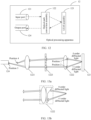
- FIG. 1a is a schematic diagram of an LCoS panel according to an embodiment of this application. Specifically, FIG. 1a may be used as an example for description.
- the LCoS panel may include a glass substrate, an ITO (indium tin oxide, indium tin oxide), two guiding layers, a liquid crystal layer, a guiding layer, a metal reflection layer, and a silicon substrate.
- a drive circuit may be deployed in the silicon substrate. The drive circuit may apply a voltage to the ITO and the metal reflection layer based on settings, so that liquid crystal molecules in the liquid crystal layer are rearranged under an action of the voltage.
- the guiding layer may ensure that the liquid crystal molecules are arranged in order under the action of the voltage.
- a refractive index of light of a position of the liquid crystal molecules is changed by rearrangement of the liquid crystal molecules, and an optical path difference is changed by changing the refractive index, so that phase modulation of light is implemented.
- different voltages may be applied to liquid crystals at different positions on the LCoS panel, so that an effect of modulating light by the LCoS panel is similar to an effect of modulating light by a blazed grating.
- the structure of the LCoS panel shown in FIG. 1a is merely an example of an LCoS panel, and an LCoS panel of another structure may also be used in this embodiment of the present invention.
- a minimum granularity of voltage control may be used as a pixel.
- liquid crystal molecules in a same pixel are controlled by a same voltage, and in this case, an effect of modulating light in the same pixel is the same. Therefore, in an actual modulation process, a phase mode loaded by the LCoS is not a standard blazed grating mode.
- diffracted light passing through the LCoS panel includes a plurality of diffraction orders.
- diffracted light of another diffraction order such as 0-order diffracted light, may be coupled to the output port, and crosstalk is caused to the system.
- FIG. 1b is a schematic diagram of an LCoS-based optical frequency domain processor according to an embodiment of this application.
- incident light input from an input port may be incident to an LCoS panel after a series of optical processing, such as deflection processing and demultiplexing and multiplexing processing, in a black solid block.
- Corresponding pixels on the LCoS diffract according to a corresponding configuration, the needed +1-order diffracted light to an output port 2 at a specific diffraction angle, and output power of the +1-order diffracted light is adjusted by using a matching degree between the +1-order diffracted light and the output port 2.
- some energy of diffracted light of another order for example, 0-order diffracted light, generated through diffraction of the LCoS may also enter the output port 2.
- a diffraction angle of the 0-order diffracted light is fixed, and output power of the 0-order diffracted light cannot be adjusted. Therefore, the 0-order diffracted light is crosstalk light for the needed +1-order diffracted light.
- diffracted light of another order may also enter another output port. As shown in FIG. 1b, -2 -order diffracted light may enter an output port 1, causing interference to an optical signal that needs to be output by the output port 1.
- the LCoS-based optical frequency domain processor usually uses a 4f optical system.
- FIG. 2 is a schematic diagram of a 4f optical system according to an embodiment of this application.
- the 4f optical system includes two lenses (a lens 1 and a lens 2) whose focal lengths are both f, a transmission grating (a grating 1), an input/output port, and an LCoS panel.
- a distance between the lens 1 and the lens 2 is 2f
- the grating 1 is disposed at a midpoint between the lens 1 and the lens 2
- the input/output port is disposed at a position that is on a side, away from the grating 1, of the lens 1 and that is f away from the lens 1
- the LCoS is disposed at a position that is on a side, away from the grating 1, of the lens 2 and that is f away from the lens 2.
- the input/output port may be different ports.
- the input/output port may be a same port which is used as an input port when receiving light input from the outside, and is used as an output port when outputting light to the outside.
- an optical path may be deflected by the lens 1. Then the incident light is demultiplexed by the grating 1, and is decomposed into light of different wavelengths. After the incident light is deflected by a lens 2, the light of different wavelengths is incident to different pixels on the LCoS panel. Diffraction angles of the light of different wavelengths are adjusted by controlling phase modulation amounts of light of the different pixels on the LCoS. Diffracted light of light of different wavelengths is converged to the output port after being deflected by the lens 2, multiplexed by the grating 1, and deflected by the lens 1. Mismatch degrees between the light of different wavelengths and the output port are different, so that adjustment and control of output power of the light of different wavelengths are implemented.
- FIG. 3a is a schematic diagram of a 4f optical system in a wavelength direction according to an embodiment of this application
- FIG. 3b is a schematic diagram of a 4f optical system in a port direction according to an embodiment of this application.
- a black solid line arrow represents light in the 4f system. It is easy to learn in FIG. 3a and FIG.
- FIG. 3b shows diffraction optical paths of light of a single wavelength at different diffraction angles.
- Light of a wavelength ⁇ 1 is used as an example. After being diffracted by the LCoS panel, the light of the wavelength ⁇ 1 may be diffracted along an optical path 1 in FIG. 3b .
- the light of the wavelength ⁇ 1 may also be diffracted along an optical path 2, an optical path 3, or an optical path 4 in FIG. 3b after being diffracted by the LCoS panel.
- the light of different wavelengths may have different diffraction angles, or may have a same diffraction angle. If the light of different wavelengths is emitted from the LCoS panel at different diffraction angles, diffracted light of different wavelengths has different incidence angles after arriving at the output port, so that matching degrees between diffracted light of different wavelengths and the output port are different. Diffracted light with a lower matching degree has smaller output power.
- the LCoS optical frequency domain processor based on the 4f system shown in FIG. 2, FIG. 3a , and FIG. 3b is an example of a structure of an optical frequency domain processor.
- the LCoS optical frequency domain processor used in this embodiment of this application may alternatively be a frequency domain processor of another construction based on the 4f system.
- an optical path may be folded or an assembly may be reused.
- the optical path is folded by replacing the grating 1 with a reflection grating, or the lens 1 and the lens 2 may be reused. Examples are not exhaustive herein.
- the diffracted light After the diffracted light is transmitted from the LCoS panel to the output port, the diffracted light matches the output port in different manners, for example, in an angle matching manner or in a displacement matching manner.
- the output port is a port having a specific cross section
- the diffracted light transmitted to the output port is a light beam having a specific cross section.
- the output port is a cylindrical port having a circular cross section
- the diffracted light is a cylindrical light beam having a circular cross section.
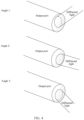
- FIG. 4 is a schematic diagram of an angle matching manner according to an embodiment of this application. As shown in FIG. 4 , in the angle matching manner, when diffracted light is transmitted to an output port, the diffracted light may be completely projected into the output port, but projection angles of the diffracted light may be different. FIG. 4 is a schematic diagram in which diffracted light is projected into an output port at three angles.
- optical power attenuation is controlled by controlling the included angle between the diffracted light and the output port.
- FIG. 5 is a schematic diagram of a displacement matching manner according to an embodiment of this application. As shown in FIG. 5 , in the displacement matching manner, when diffracted light is transmitted to an output port, an included angle between the diffracted light and the output port remains unchanged, but an axis of the diffracted light and the axis of the output port may have deviations of different displacements. FIG. 5 is a schematic diagram in which diffracted light is projected into an output port in three displacements of axises.
- diffracted light corresponding to a displacement 1, a displacement 2, and a displacement 3 may have axises parallel to the axis of the output port, but axises of diffracted light corresponding to the displacement 1 and the displacement 2 have deviations of large displacements from the axis of the output port, so that a part of the diffracted light cannot be projected into the output port, causing a large loss. Therefore, optical power attenuation is controlled by controlling the deviation displacements between axises of the diffracted light and the output port.
- the angle matching manner may be implemented by disposing the output port at a position that is on a side, away from the grating 1, of the lens 1 and that is f away from the lens 1 in the 4f system as shown in FIG. 2 . It can be learned from FIG. 3b that, after diffracted light with different diffraction angles is transmitted to the output port, included angles between the diffracted light and the output port may be different, so that optical power is adjusted in the angle matching manner.
- the displacement matching manner may be implemented by using a 4f system shown in FIG. 6.
- FIG. 6 is a schematic diagram of an apparatus for the displacement matching manner according to an embodiment of this application. As shown in FIG.
- FIG. 7 is a schematic diagram of another 4f optical system in a port direction according to an embodiment of this application.
- FIG. 7 shows an optical path of the system in FIG. 6 in the port direction.
- diffracted light at different diffraction angles may be deflected by the lens 3 to have deviations of different displacements from an axis of an input/output port, so that optical power is adjusted in the displacement matching manner.
- angle matching manner or displacement matching manner is intended to adjust power intensity of +1-order diffracted light generated by the LCoS panel, and control an angle matching degree and a displacement matching degree between the +1-order diffracted light and the output port.
- the LCoS panel diffracts light, diffracted light of another diffractive order such as 0-order diffracted light is further generated.
- a diffraction angle of the 0-order diffracted light is equal to an incidence angle. Therefore, when the incidence angle is fixed, the diffraction angle of the 0-order diffracted light remains unchanged, and a diffraction angle of the +1-order diffracted light is adjustable.
- an optimal diffraction angle that enables highest coupling efficiency and lowest coupling loss of light in a process in which light is transmitted from the LCoS panel to the output port may be determined. That is, if the light is emitted from the LCoS panel at the optimal diffraction angle, power of the light finally transmitted to the output port is the largest. For example, in the angle matching manner, if light is diffracted from the LCoS at the optimal diffraction angle, when the diffracted light finally arrives at the output port, an included angle between the diffracted light and the output port is the smallest, so that the loss of the diffracted light is the lowest.
- the displacement matching manner if the light is diffracted from the LCoS at the optimal diffraction angle, when the diffracted light finally arrives at the output port, a displacement of the deviation between the axis of the diffracted light and the axis of the output port is the smallest, so that the coupling loss of the diffracted light is the lowest. If a diffraction angle of light emitted from the LCoS panel is greater than the optimal diffraction angle or less than the optimal diffraction angle, the power of the light finally transmitted to the output port is attenuated, and the coupling loss of the light is increased. Refer to FIG. 8 and FIG. 9 . Impact of different diffraction angles on output optical power is further described.
- FIG. 8 is a schematic diagram of a principle of coupling between diffracted light and an output port in a case of small attenuation according to an embodiment of this application.
- FIG. 9 is a schematic diagram of a principle of coupling between diffracted light and an output port in a case of large attenuation according to an embodiment of this application.
- Diffraction efficiency shown in 8(a) in FIG. 8 and 9(a) in FIG. 9 may be a ratio of intensity of light diffracted from an LCoS to intensity of light incident to the LCoS.
- +1-order diffracted light concentrates most energy of the diffracted light, and diffraction efficiency of the +1-order diffracted light is higher than diffraction efficiency of 0-order diffracted light.
- a diffraction angle of the 0-order diffracted light is equal to an incidence angle of the light on the LCoS. Because the incidence angle of the light on the LCoS remains unchanged, the diffraction angle of the 0-order diffracted light is unadjustable (where a diffraction angle of the 0-order diffracted light in FIG. 8 is the same as a diffraction angle of the 0-order diffracted light in FIG. 9 ).
- a diffraction angle of the +1-order diffracted light is related to factors such as an incidence angle of the light on the LCoS, whether the incident light on the LCoS and a diffraction angle of the +1-order diffracted light are on a same side of a normal of the LCoS, and a wavelength of the light. Therefore, the diffraction angle of the +1-order diffracted light is adjustable, but adjustment of the diffraction angle of the +1-order diffracted light does not affect diffraction efficiency of the +1-order diffracted light (where a diffraction angle of the +1-order diffracted light in FIG. 8 is less than a diffraction angle of the +1-order diffracted light in FIG. 9 , and diffraction efficiency of the +1-order diffracted light in FIG. 8 and FIG. 9 remains unchanged).
- ⁇ c in 8(b) in FIG. 8 and 9(b) in FIG. 9 is an optimal diffraction angle.
- a change of optical coupling efficiency with the diffraction angle may be represented by a solid line in a coordinate system in 8(b) in FIG. 8 or 9(b) in FIG. 9 .
- Optical coupling efficiency corresponding to the optimal diffraction angle is the highest, and within a specific range, the larger a deviation from the optimal diffraction angle, the lower the optical coupling efficiency (where when the deviation exceeds the specific range, the optical coupling efficiency may be 0).
- output optical power (which may be represented by a wave peak on the right side of a solid line in the coordinate system in 8(c)) of the +1-order diffracted light in 8(c) in the case of small attenuation shown in FIG. 8 is higher than output optical power (which may be represented by a wave peak on the right side of a solid line in the coordinate system in 9(c)) of the +1-order diffracted light in 9(c) in the case of large attenuation shown in FIG. 9 .
- the +1-order diffracted light is used as required signal light.
- output optical power of the +1-order diffracted light is small; and in a case of small attenuation, output optical power of the +1-order diffracted light is large.
- the 0-order diffracted light is used as crosstalk light.
- the 0-order diffracted light is equivalent to background noise introduced in an optical frequency domain processor, and reduces purity of the output light.
- the 0-order diffracted light is sensitive to a system parameter, and has poor power stability. This causes a large power jitter of the output light, and reduces stability of output optical power of the optical frequency domain processor.
- FIG. 10 is a schematic diagram of impact of crosstalk light on power stability of an optical frequency domain processor according to an embodiment of this application.
- 10(a) shows that when the crosstalk light is large, output optical power jitter amplitude of the optical frequency domain processor is large
- 10(b) shows that when the crosstalk light is small, output optical power jitter amplitude of the optical frequency domain processor is small.
- optical power that can be output by the optical frequency domain processor is determined.
- minimum optical power that can be output by the optical frequency domain processor is related to crosstalk light such as the 0-order diffracted light. Because optical power of the 0-order diffracted light is not adjustable, if the optical power of the 0-order diffracted light is excessively large, the minimum optical power that can be output by the frequency domain processor is excessively large, so that an adjustable attenuation range of the optical power output by the optical frequency domain processor is reduced.
- FIG. 11 may be used as an example. FIG.
- 11 is a schematic diagram of impact of crosstalk light on an adjustable attenuation range of an optical frequency domain processor according to an embodiment of this application.
- 11(a) shows that when the crosstalk light is large, the adjustable attenuation range of the optical frequency domain processor is small
- 11(b) shows that when the crosstalk light is small, the adjustable attenuation range of the optical frequency domain processor is large.
- the optical processing apparatus may be an optical frequency domain processor, or may be a part of an optical frequency domain processor, and can suppress crosstalk light such as 0-order diffracted light, to improve stability of output optical power of the optical frequency domain processor and increase an adjustable attenuation range of the optical frequency domain processor.
- FIG. 12 is a schematic diagram of a structure of an optical processing apparatus according to an embodiment of this application.
- the optical processing apparatus 12 includes an input port 121, an optical path conversion assembly 122, an LCoS assembly 123, and an output port 124.
- the input port 121 is configured to receive a first light beam.
- the optical path conversion assembly 122 is configured to disperse the first light beam to obtain a second light beam, where the second light beam is a single-wavelength light beam.
- the LCoS assembly 123 is configured to diffract the second light beam to obtain diffracted light of the second light beam, where the LCoS assembly includes a plurality of pixels, light beams received by the plurality of pixels correspond to different diffraction angles, the diffraction angles are used to control an attenuation degree of the light beams received by the pixels in the optical processing apparatus, and the diffracted light of the second light beam includes 0-order diffracted light and +1-order diffracted light.
- the optical path conversion assembly 122 is further configured to: transmit the diffracted light of the second light beam, and converge the +1-order diffracted light to the output port, where a deflection capability of the optical path conversion assembly 122 for the 0-order diffracted light is different from a deflection capability for the +1-order diffracted light.
- the output port 124 is configured to output the received +1-order diffracted light in a collimated manner.
- the LCoS assembly 123 diffracts the second light beam to obtain diffracted light of a plurality of diffractive orders of the second light beam. Then the diffracted light of the second light beam is transmitted by using the optical path conversion assembly 122, the +1-order diffracted light that is used as the signal light is transmitted to the output, and the +1-order diffracted light that is converged to the output port 124 is output by the output port 124 in a collimated manner.
- the optical path conversion assembly 122 transmits the diffracted light
- the optical path conversion assembly 122 can converge the +1-order diffracted light to the output port 124
- the 0-order diffracted light is partially or completely deviated from the output port 124, and a loss of the 0-order diffracted light is generated.
- the loss of the 0-order diffracted light relieves problems, caused by crosstalk light, of poor stability of the optical frequency domain processor and a small adjustable attenuation range of the optical frequency domain processor.
- the input port 121 is configured to receive a first light beam.
- the optical path conversion assembly 122 is configured to disperse the first light beam to obtain a second light beam, where the second light beam is a single-wavelength light beam.
- the LCoS assembly 123 is configured to diffract the second light beam to obtain diffracted light of the second light beam, where the LCoS assembly includes a plurality of pixels, light beams received by the plurality of pixels correspond to different diffraction angles, the diffraction angles are used to control an attenuation degree of the light beams received by the pixels in the optical processing apparatus, and the diffracted light of the second light beam includes 0-order diffracted light and +1-order diffracted light.
- the optical path conversion assembly 122 is further configured to: transmit the diffracted light of the second light beam, and converge the +1-order diffracted light to the output port, where a transmittance capability of the optical path conversion assembly 122 for the +1-order diffracted light is higher than a transmittance capability for the 0-order diffracted light.
- the output port 124 is configured to output the received +1-order diffracted light in a collimated manner.
- the LCoS assembly 123 diffracts the second light beam to obtain diffracted light of a plurality of diffractive orders of the second light beam. Then the diffracted light of the second light beam is transmitted by using the optical path conversion assembly 122, the +1-order diffracted light that is used as the signal light is transmitted to the output, and the +1-order diffracted light that is converged to the output port 124 is output by the output port 124 in a collimated manner.
- a transmittance capability of the optical path conversion assembly for the +1-order diffracted light is higher than a transmittance capability for the 0-order diffracted light, so that the 0-order diffracted light is suppressed in a process of being transmitted to the output port, and a loss of the 0-order diffracted light is generated.
- the loss of the 0-order diffracted light relieves problems, caused by crosstalk light, of poor stability of the optical frequency domain processor and a small adjustable attenuation range of the optical frequency domain processor.
- optical processing apparatus 12 shown in FIG. 12 . It should be noted that the following related descriptions may be corresponding to the optical processing apparatus 12 that is applicable to any one of the foregoing functions.
- the first light beam may be a single-wavelength light beam, or may be a multi-wavelength light beam. If the first light beam is a single-wavelength light beam, after the optical path conversion assembly 122 disperses the first light beam, a second light beam is obtained; if the first light beam is a multi-wavelength light beam, after the optical path conversion assembly 122 disperses the first light beam, a plurality of single-wavelength light beams with different wavelengths may be obtained, and any single-wavelength light beam may be used as a second light beam. In this way, crosstalk, such as the 0-order diffracted light, on the optical processing apparatus 12 in this embodiment of this application can be reduced.
- the first light beam is dispersed into a plurality of single-wavelength light beams with different wavelengths, frequencies of the single-wavelength light beams are different, so that the first light beam is decomposed in frequency domain, and processing of the single-wavelength light beam implements processing of the first light beam in frequency domain.
- the input port 121 may include an optical fiber collimator, which may change a diverged light beam into a collimated light beam.
- the output port 124 may include an optical fiber collimator.
- the input port 121 and the output port 124 may share a same optical fiber collimator.
- An optical circulator inputs, in a collimated manner, a light beam input from the input port 121 into the optical processing apparatus 12, and outputs, in a collimated manner, a light beam received from the optical processing apparatus 12 to outside of the optical processing apparatus 12.
- the input port 121 and the output port 124 may share a same port.
- the port When the received light beam is input into the optical processing apparatus 12 in a collimated manner, the port is used as the input port 121. When the received light beam is output from the optical processing apparatus 12 in a collimated manner, the port is used as the output port 124.
- the optical path conversion assembly 122 may include a first deflection component 1221, a second deflection component 1222, and a demultiplexing/multiplexing component 1223.
- the demultiplexing/multiplexing component 1223 is configured to disperse the first light beam passing through the first deflection component 1221 to obtain the second light beam; and the second deflection component 1222 is configured for incidence of the second light beam into the LCoS assembly.
- the first deflection component 1221 may include one convex lens or a combination of a plurality of convex lenses, and the first deflection component 1221 may further include one concave reflector or a combination of a plurality of concave reflectors.
- the second deflection component 1222 may include one convex lens or a combination of a plurality of convex lenses, and the second deflection component 1222 may further include one concave reflector or a combination of a plurality of concave reflectors.
- the demultiplexing/multiplexing component 1223 may be a grating.
- the first deflection component 1221, the second deflection component 1222, and the demultiplexing/multiplexing component 1223 in the optical path conversion assembly 122 may have a plurality of alternative implementations to implement the loss of crosstalk light such as 0-order diffracted light.
- the following describes five alternative implementations as examples.
- two optional implementations are further described as examples.
- That deflection capabilities for a light beam are different may include that deflection effects are different and/or that deflection intensities are different.
- the deflection effect may include a convergence effect and a divergence effect. Therefore, in the first to third alternative implementations, the optical path deflection assembly may have different implementations based on different deflection capabilities.
- the 0-order diffracted light is illuminated at a first position on the second deflection component 1222.
- the +1-order diffracted light is illuminated at a second position on the second deflection component 1222.
- the first position and the second position on the second deflection component 1222 have different deflection capabilities for a same light beam.
- an illumination position of the 0-order diffracted light on the first deflection component 1221 is a third position
- an illumination position of the +1-order diffracted light on the first deflection component 1221 is a fourth position.
- the third position and the fourth position on the first deflection component 1221 have different deflection capabilities for a same light beam.
- different deflection capabilities for the same light beam at different positions on the first deflection component 1221 or the second deflection component 1222 may alternatively be implemented in different optional manners.
- deflection effects of the first deflection component 1221 and/or the second deflection component 1222 on the +1-order diffracted light and the 0-order diffracted light are convergence effects, and a convergence capability for the +1-order diffracted light is different from a deflection intensity on the 0-order diffracted light (where in a case in which the deflection effect on the light beam is the convergence effect, the deflection intensity is also convergence intensity).
- the second deflection component 1222 is used as an example.
- the second deflection component 1222 is a convex lens, and curvature radii (or spherical aberrations) of a first position and a second position are different, so that different deflection intensities on the +1-order diffracted light and the 0-order diffracted light may be implemented.
- the curvature radius of the first position may be greater than the curvature radius of the second position, or the curvature radius of the first position may be less than the curvature radius of the second position.
- the second deflection component 1222 is a lens with a uniform curvature radius, and an assembly having a specific deflection capability for the light beam may be disposed in front of the first position or in front of the second position (or behind the first position or behind the second position, where "in front of” and “behind” herein may be understood based on a transmission direction of the light beam, a position at which the light beam arrives first is “front”, and a position at which the light beam arrives later is "behind"), so that the lens has different deflection intensities on the +1-order diffracted light and the 0-order diffracted light. In this way, the +1-order diffracted light may be converged to the output port 124, and a part or all of the 0-order diffracted light is deviated from the output port 124; or the like.
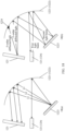
- FIG. 13a to FIG. 14 are schematic diagrams of suppression of crosstalk light by asymmetric spherical aberration deflection components according to embodiments of this application. Specifically, FIG. 13a to FIG. 14 may be used as examples for description. To simplify views, the input port 121 and an optical path in which a light beam is transmitted from the input port 121 to the LCoS assembly 123 are omitted in FIG. 13a to FIG. 14 , and only an optical path in which a light beam is transmitted from the LCoS assembly 123 to the output port 124 is shown.
- an illumination position of the 0-order diffracted light diffracted by the LCoS assembly 123 on the second deflection component 1222 is a position 1
- an illumination position of the +1-order diffracted light diffracted by the LCoS assembly 123 on the second deflection component 1222 is a position 2
- a curvature radius of the position 1 on the second deflection component 1222 is greater than a curvature radius of the position 2.
- the deflection intensity of the second deflection component 1222 on the 0-order diffracted light is greater than the deflection intensity on the +1-order diffracted light, so that the +1-order diffracted light may converge at a position 3 of the output port 124, and the 0-order diffracted light may converge at a position 4 between the output port 124 and the first deflection component 1221. Because energy of the light beam at a convergence position after passing through the lens is the most concentrated, and after passing through the convergence position, the light beam starts to diverge again, the +1-order diffracted light converges at the position 3 of the output port 124, which facilitates output of the light beam.
- the 0-order diffracted light continues to diverge in a process of transmitting forward.
- a possible case is that the 0-order diffracted light is completely staggered with the output port 124, and is no longer output from the output port, so that crosstalk on the signal light is reduced; and another possible case is that, after the 0-order diffracted light is diverged, only a part of the light beam may be emitted into the output port 124, and a remaining part of the light beam cannot be emitted into the output port 124, so that a crosstalk degree on the signal light is reduced.
- the second deflection component 1222 in FIG. 13a may be replaced by a lens with a uniform curvature radius and a transparent glass sheet with an unequal thickness in FIG. 13b or FIG. 13c , so that deflection intensity on the 0-order diffracted light can also be greater than deflection intensity on the +1-order diffracted light.
- this is not exhaustive.
- an illumination position of the 0-order diffracted light diffracted by the LCoS assembly 123 on the second deflection component 1222 is a position 5
- an illumination position of the diffracted +1-order diffracted light on the second deflection component 1222 is a position 6
- a curvature radius of the position 5 on the second deflection component 1222 is less than a curvature radius of the position 6.
- the deflection intensity of the second deflection component 1222 on the 0-order diffracted light is less than the deflection intensity on the +1-order diffracted light, so that the +1-order diffracted light may converge at a position 7 of the output port 124, and the 0-order diffracted light may converge at a position 8 on a side that is of the output port 124 and that is away from the first deflection component 1221.
- the 0-order diffracted light does not converge to one point before being transmitted to a plane in which an end surface of the output port 124 is located.
- the second deflection component 1222 in FIG. 14 may alternatively be replaced by a lens with a uniform curvature radius and a transparent glass sheet with an unequal thickness. Details are not described herein again.
- Examples in FIG. 13a to FIG. 14 describe examples in which the first position and the second position in the second deflection component 1222 have different deflection capabilities for a same light beam.
- a principle of a specific optical path in which the third position and the fourth position in the first deflection component 1221 have different deflection capabilities for a same light beam is similar to principles of the foregoing two examples. Details are not described herein again.
- a deflection effect of the first deflection component 1221 and/or the second deflection component 1222 on the 0-order diffracted light is a divergence effect
- a deflection effect on the +1-order diffracted light is a convergence effect
- the second deflection component 1222 is used as an example.
- a deflection effect of the first position on the second deflection component 1222 on the light beam is a divergence effect
- a deflection effect of the second position on the second deflection component 1222 on the light beam is a convergence effect.
- the first position may be a concave lens
- the second position may be a convex lens.
- FIG. 15 is a schematic diagram of suppression of crosstalk light by a deflection component with an asymmetric deflection effect according to an embodiment of this application.
- an illumination position of the 0-order diffracted light diffracted by the LCoS assembly 123 on the second deflection component 1222 is a position 9
- an illumination position of the diffracted +1-order diffracted light on the second deflection component 1222 is a position 10.
- the position 9 on the second deflection component 1222 is a concave lens
- the position 10 is a convex lens.
- the second deflection component 1222 has a divergence effect on the 0-order diffracted light and a convergence effect on the +1-order diffracted light.
- the +1-order diffracted light may converge at the position 11 of the output port 124, and the 0-order diffracted light is diverged into an optical path outside the output port 124, so that the 0-order diffracted light is not transmitted into the output port 124 and causes crosstalk to the signal light.
- the first position may be a convex reflector
- the second position may be a concave reflector. Examples are not described herein again.
- the first position and the second position on the second deflection component 1222 have different deflection capabilities for a same light beam
- the third position and the fourth position on the first deflection component 1221 have different deflection capabilities for a same light beam.
- the second deflection component 1222 and the first deflection component 1221 deflect the 0-order diffracted light and the +1-order diffracted light, so that the +1-order diffracted light converges to the output port 124, and a convergence position of the 0-order diffracted light does not completely overlap the output port 124.
- the optical path conversion assembly 122 may further have alternative implementations based on different transmittance capabilities.
- a first suppression element 1224 is disposed on one or more of the first deflection component 1221, the second deflection component 1222, and the demultiplexing/multiplexing component 1223, and the first suppression element 1224 is configured to suppress the 0-order diffracted light.
- the optical path conversion assembly 122 suppresses the 0-order diffracted light by using the first suppression element 1224, so that a transmittance capability for the +1-order diffracted light is higher than a transmittance capability for the +1-order diffracted light.
- the first suppression element 1224 may be disposed on any of the foregoing components through adherence or the like.
- the first suppression element 1224 may suppress a part or all of the 0-order diffracted light.
- the first suppression element 1224 may be a light shielding plate.
- the first suppression element 1224 may be an optical filter that has a function of filtering a part or all of the 0-order diffracted light.
- FIG. 16 is a schematic diagram of suppression of crosstalk light by a first suppression element according to an embodiment of this application. FIG. 16 may be used as an example for description.
- the first suppression element 1224 is a light shielding plate
- the first deflection component 1221 includes a lens and a uniform light-transmitting glass sheet
- the first suppression element 1224 is disposed in front of the uniform light-transmitting glass sheet of the first deflection component 1221 to block transmission of the 0-order diffracted light, so that the 0-order diffracted light is prevented from being transmitted into the output port 124 to cause crosstalk to the signal light.
- a transmittance capability of the optical path conversion assembly 122 for the +1-order diffracted light is higher than a transmittance capability for the 0-order diffracted light, and the optical path conversion assembly has different deflection capabilities for the 0-order diffracted light and for the +1-order diffracted light, so that a loss of the 0-order diffracted light is implemented.
- a suppression element is disposed on the second deflection component 1222 in the optical path conversion assembly 122.
- the suppression element is configured to attenuate the 0-order diffracted light to a specific extent, and the first deflection component 1221 has a convergence effect on the +1-order diffracted light, so that the +1-order diffracted light converges to the output port.
- the first deflection component 1221 has a divergent effect on the 0-order diffracted light, and further implements the loss of the 0-order and the diffracted light. In this way, the loss of the 0-order diffracted light is implemented by controlling both the transmittance capability and the deflection capability.
- specific implementations in the first to third alternative implementations may be combined with the fourth alternative implementation, to obtain more specific implementations in the fifth alternative implementation. This is not exhaustively listed herein.
- focal lengths of the first deflection component 1221 and the second deflection component 1222 are a first focal length
- a position of the first suppression element 1224 may be determined based on the first focal length and an incidence angle of the second light beam on the LCoS assembly.
- components in the optical processing apparatus 12 may constitute a 4f system.
- Focal lengths of the first deflection component 1221 and the second deflection component 1222 are both f.
- a distance between the input port 121 and the first deflection component 1221, a distance between the first deflection component 1221 and the demultiplexing/multiplexing component 1223, a distance between the demultiplexing/multiplexing component 1223 and the second deflection component 1222, and a distance between the second deflection component 1222 and the LCoS assembly are all f. It should be understood that cases such as element sharing and optical path folding may exist in the 4f system.
- a diffraction angle (namely, a first diffraction angle) with the highest coupling efficiency and the lowest coupling loss in a process in which light is transmitted from the LCoS panel to the output port may be determined.
- a diffraction angle of the +1-order diffracted light in the LCoS assembly is equal to the first diffraction angle, the +1-order diffracted light has the lowest coupling loss in a process from being emitted from the LCoS assembly to being output by the output port in a collimated manner.
- the first diffraction angle refer to the foregoing descriptions of the optimal diffraction angle, and details are not described herein again.
- a diffraction angle of the 0-order diffracted light on the LCoS is less than the first diffraction angle, and a diffraction angle of the +1-order diffracted light on the LCoS assembly is greater than or equal to the first diffraction angle; or a diffraction angle of the 0-order diffracted light on the LCoS assembly is greater than the first diffraction angle, and a diffraction angle of the +1-order diffracted light on the LCoS assembly is greater than or equal to the first diffraction angle.
- the diffracted light of the second light beam may further include diffracted light of a diffraction order such as +2-order diffracted light.
- an angle between the +2-order diffracted light and the +1-order diffracted light diffracted from the LCoS is approximately equal to twice an angle between the +1-order diffracted light and the 0-order diffracted light diffracted from the LCoS, diffraction angles of the 0-order diffracted light and the +1-order diffracted light are distributed on the two sides of the first diffraction angle, so that a distance between diffracted light of a diffraction order such as the +2-order diffracted light and the +1-order diffracted light is longer, and crosstalk to the +1-order diffracted light is reduced.
- FIG. 17 may be used as an example for description.
- FIG. 17 is a schematic diagram of an adjustable attenuation range of an optical processing apparatus according to an embodiment of this application. 17(a) in FIG.
- 17 shows an adjustable attenuation range of the optical processing apparatus 12 when the optical path conversion assembly 122 is shown in the first or second alternative implementation in this embodiment of this application
- 17(b) shows an adjustable attenuation range of the optical processing apparatus 12 when the optical path conversion assembly 122 is shown in the fourth alternative implementation in this embodiment of this application.
- ⁇ c is an optimal diffraction angle
- the right side of ⁇ c is the adjustable attenuation range (namely, an adjustable range of a diffraction angle of the +1-order diffracted light) of the optical processing apparatus 12.
- the diffraction angle of the 0-order diffracted light is distributed on the left side of ⁇ c, and the loss of the 0-order diffracted light is achieved by reducing optical coupling efficiency on the left side of ⁇ c.
- the incidence angle of the second light beam on the LCoS assembly is greater than zero, so that after the second light beam is incident on the LCoS assembly at a zero-degree incidence angle, 0-order diffracted light is prevented from returning in an original path at the zero-degree diffraction angle, and a situation that causes crosstalk to the signal light is avoided.
- FIG. 18 , FIG. 19(a), and FIG. 19(b) are schematic diagrams of structures of other optical processing apparatuses according to embodiments of this application.
- an input port 121 and an output port 124 share a same port, a first deflection component 1221 and a second deflection component 1222 in an optical path conversion assembly 122 share a same concave reflector, and a first suppression element 1224 is disposed on the concave reflector.
- an input port 121 and an output port 124 share a same port, a first deflection component 1221 and a second deflection component 1222 in an optical path conversion assembly 122 share a same convex lens, and a first suppression element 1224 is disposed on the convex lens.
- 18(a) and FIG. 19(a) respectively show optical paths of the two optical processing apparatuses in the wavelength direction.
- a first light beam received by the input port 121 is dispersed into a plurality of single-wavelength light beams by the demultiplexing/multiplexing component 1223.
- 18 (a) and FIG. 19 (a) show three single-wavelength light beams (represented by ⁇ 1, ⁇ 2, and ⁇ 3 respectively) in examples.
- 18(b) and FIG. 19(b) show optical paths of the two optical processing apparatuses in the port direction. Any single-wavelength light beam obtained by the demultiplexing/multiplexing component 1223 through dispersion may be considered as a second light beam.
- the second light beam is illuminated on the LCoS assembly and is diffracted.
- the 0-order diffracted light is diffracted from the LCoS assembly, the 0-order diffracted light is illuminated on the first suppression element 1224.
- the first suppression element 1224 blocks transmission of the 0-order diffracted light, to implement attenuation of the 0-order diffracted light, and reduce crosstalk of the 0-order diffracted light to +1-order diffracted light.
- FIG. 18 , FIG. 19(a), and FIG. 19(b) are merely used to describe how the optical processing apparatus in embodiments of this application implements, in a case of optical path folding or element sharing, that a projection capability of the optical path conversion assembly for +1-order diffracted light is higher than a projection capability for 0-order diffracted light, or that a deflection capability of the optical path conversion assembly for the +1-order diffracted light is different from a deflection capability for the 0-order diffracted light.
- This does not represent all solutions for implementing the foregoing functions defined in this application. There are still a plurality of other solutions.
- FIG. 18 and FIG. 19(a) and FIG. 19(b) each show an angle matching manner.
- FIG. 18 , FIG. 19(a), and FIG. 19(b) each show a manner in which transmission of the 0-order diffracted light is blocked by the first suppression element 1224.
- the second deflection component 1222 in FIG. 18 may be designed to be a concave reflector with an uneven curvature radius, or the second deflection component 1222 in FIG. 19(a) and FIG.
- 19(b) may be designed to be a convex lens with an uneven spherical aberration, to implement that the +1-order diffracted light is transmitted and converged to the output port, and that the 0-order diffracted light is reflected or refracted to a position that deviates from the output port. All manners are not exhaustively listed herein.
- An embodiment of this application further provides an optical system.
- the optical system is configured to process an input first light beam in frequency domain, and output a light beam obtained through processing.
- the optical system may be a tunable optical filter, and may filter light of a specific wavelength (or frequency) in the first light beam, and output a filtered light beam.
- the optical system may be an optical signal power equalizer, and may perform power adjustment on light of each wavelength (or frequency) in the first light beam, and output a light beam whose power is adjusted.
- the optical system may be a wavelength selective switch, and may screen light of a specified wavelength (or frequency) in the first light beam, and output a light beam obtained through screening.
- the optical processing apparatus may be the optical processing apparatus corresponding to any one of FIG. 12 to FIG. 16 or FIG. 18 , FIG. 19(a), and FIG. 19(b) in embodiments of this application, to reduce crosstalk caused by 0-order diffracted light to signal light in the optical system.
- A/B may represent A or B.
- and/or describes only an association relationship for describing associated objects and may represent that three relationships may exist.
- a and/or B may represent the following three cases: Only A exists, both A and B exist, and only B exists.
- the term "a plurality of" means two or more than two.
Landscapes
- Physics & Mathematics (AREA)
- General Physics & Mathematics (AREA)
- Optics & Photonics (AREA)
- Nonlinear Science (AREA)
- Chemical & Material Sciences (AREA)
- Crystallography & Structural Chemistry (AREA)
- Engineering & Computer Science (AREA)
- Computer Networks & Wireless Communication (AREA)
- Optical Couplings Of Light Guides (AREA)
- Optical Modulation, Optical Deflection, Nonlinear Optics, Optical Demodulation, Optical Logic Elements (AREA)
Applications Claiming Priority (2)
| Application Number | Priority Date | Filing Date | Title |
|---|---|---|---|
| CN202011349303.6A CN114545557A (zh) | 2020-11-26 | 2020-11-26 | 一种光处理装置及光学系统 |
| PCT/CN2021/129561 WO2022111276A1 (fr) | 2020-11-26 | 2021-11-09 | Dispositif de traitement optique et système optique |
Publications (3)
| Publication Number | Publication Date |
|---|---|
| EP4246196A1 true EP4246196A1 (fr) | 2023-09-20 |
| EP4246196A4 EP4246196A4 (fr) | 2024-05-08 |
| EP4246196B1 EP4246196B1 (fr) | 2026-01-07 |
Family
ID=81668250
Family Applications (1)
| Application Number | Title | Priority Date | Filing Date |
|---|---|---|---|
| EP21896777.6A Active EP4246196B1 (fr) | 2020-11-26 | 2021-11-09 | Dispositif de traitement optique et système optique |
Country Status (4)
| Country | Link |
|---|---|
| US (1) | US20230296842A1 (fr) |
| EP (1) | EP4246196B1 (fr) |
| CN (1) | CN114545557A (fr) |
| WO (1) | WO2022111276A1 (fr) |
Families Citing this family (3)
| Publication number | Priority date | Publication date | Assignee | Title |
|---|---|---|---|---|
| CN112737683B (zh) * | 2019-10-14 | 2023-05-16 | 华为技术有限公司 | 功率均衡器及功率均衡器的调节方法 |
| US12345998B2 (en) * | 2022-06-03 | 2025-07-01 | Ii-Vi Delaware, Inc. | Tunable optical wedge for reducing crosstalk in wavelength selective switch |
| WO2024011521A1 (fr) * | 2022-07-14 | 2024-01-18 | 华为技术有限公司 | Commutateur sélectif en longueur d'onde et procédé de modulation de faisceau lumineux |
Family Cites Families (16)
| Publication number | Priority date | Publication date | Assignee | Title |
|---|---|---|---|---|
| KR100815345B1 (ko) * | 2004-12-02 | 2008-03-19 | 삼성전기주식회사 | 회절광과 조명광을 분리한 칼라 디스플레이 장치 |
| US7822303B2 (en) * | 2005-09-08 | 2010-10-26 | Oclaro (New Jersey), Inc. | Optical wavelength selective router |
| JP4651635B2 (ja) * | 2007-03-29 | 2011-03-16 | 富士通株式会社 | 波長選択スイッチ |
| JP2009128578A (ja) * | 2007-11-22 | 2009-06-11 | Fujitsu Ltd | 波長選択スイッチ |
| US7676126B2 (en) * | 2007-12-12 | 2010-03-09 | Jds Uniphase Corporation | Optical device with non-equally spaced output ports |
| JP5040842B2 (ja) * | 2008-07-24 | 2012-10-03 | 富士通株式会社 | 波長選択スイッチ |
| US8659835B2 (en) * | 2009-03-13 | 2014-02-25 | Optotune Ag | Lens systems and method |
| US8300995B2 (en) * | 2010-06-30 | 2012-10-30 | Jds Uniphase Corporation | M X N WSS with reduced optics size |
| WO2012115077A1 (fr) * | 2011-02-24 | 2012-08-30 | オリンパス株式会社 | Commutateur de sélection de longueur d'onde |
| JP6019466B2 (ja) * | 2012-07-17 | 2016-11-02 | サンテック株式会社 | 波長選択光スイッチ装置 |
| US8977079B2 (en) * | 2012-07-18 | 2015-03-10 | Jds Uniphase Corporation | WSS with high port isolation and close spaced ports |
| JP2014215457A (ja) * | 2013-04-25 | 2014-11-17 | 住友電気工業株式会社 | 波長選択スイッチ |
| JP5981903B2 (ja) * | 2013-11-08 | 2016-08-31 | 日本電信電話株式会社 | 光スイッチ |
| JP2016020935A (ja) * | 2014-07-11 | 2016-02-04 | 株式会社リコー | レーザー装置 |
| WO2016106521A1 (fr) * | 2014-12-29 | 2016-07-07 | 华为技术有限公司 | Commutateur de sélection de longueurs d'onde |
| US10042121B1 (en) * | 2017-03-28 | 2018-08-07 | Nistica, Inc. | Toroidal micro lens array for use in a wavelength selective switch |
-
2020
- 2020-11-26 CN CN202011349303.6A patent/CN114545557A/zh active Pending
-
2021
- 2021-11-09 EP EP21896777.6A patent/EP4246196B1/fr active Active
- 2021-11-09 WO PCT/CN2021/129561 patent/WO2022111276A1/fr not_active Ceased
-
2023
- 2023-05-25 US US18/323,453 patent/US20230296842A1/en active Pending
Also Published As
| Publication number | Publication date |
|---|---|
| US20230296842A1 (en) | 2023-09-21 |
| EP4246196A4 (fr) | 2024-05-08 |
| CN114545557A (zh) | 2022-05-27 |
| EP4246196B1 (fr) | 2026-01-07 |
| WO2022111276A1 (fr) | 2022-06-02 |
Similar Documents
| Publication | Publication Date | Title |
|---|---|---|
| US20230296842A1 (en) | Optical processing apparatus and optical system | |
| JP5899331B2 (ja) | 光入出力装置 | |
| JP6150146B2 (ja) | ビーム処理装置、ビーム減衰および切り替え装置、ならびに光波長選択スイッチシステム | |
| US6801310B2 (en) | Liquid crystal modulator and polarization diversity optics for optical communications | |
| GB2504970A (en) | Optical device and methods to reduce cross-talk | |
| US11307354B2 (en) | Wavelength selective switch based on LCoS | |
| US7376311B2 (en) | Method and apparatus for wavelength-selective switches and modulators | |
| US11728919B2 (en) | Optical communications apparatus and wavelength selection method | |
| US9977190B2 (en) | Wavelength selective switch | |
| JP7479518B2 (ja) | 光交換装置、リダイレクション方法、リコンフィギュラブル光アド/ドロップマルチプレクサ、及びシステム | |
| CN101718938A (zh) | 色散控制模块和波长阻隔器 | |
| WO2025123926A1 (fr) | Modulateur spatial de lumière, commutateur sélectif en longueur d'onde, dispositif de communication optique et système | |
| CN202512293U (zh) | 一种基于tff宽范围内可调谐光滤波器 | |
| Marom et al. | Filter-shape dependence on attenuation mechanism in channelized dynamic spectral equalizers | |
| JP5086317B2 (ja) | 可変分散補償器 | |
| JP2012168285A (ja) | 波長選択スイッチ | |
| CN216670325U (zh) | 一种新型窄带光可调光滤波器 | |
| CN116466496A (zh) | 一种偏振分光及转换器件及波长选择开关 | |
| JP2017102404A (ja) | 波長選択スイッチおよび波長選択方法 | |
| Seno et al. | Wide-passband 88-wavelength channel-by-channel tunable optical dispersion compensator with 50-GHz spacing | |
| CA2390768A1 (fr) | Compensateur de dispersion accordable |
Legal Events
| Date | Code | Title | Description |
|---|---|---|---|
| STAA | Information on the status of an ep patent application or granted ep patent |
Free format text: STATUS: THE INTERNATIONAL PUBLICATION HAS BEEN MADE |
|
| PUAI | Public reference made under article 153(3) epc to a published international application that has entered the european phase |
Free format text: ORIGINAL CODE: 0009012 |
|
| STAA | Information on the status of an ep patent application or granted ep patent |
Free format text: STATUS: REQUEST FOR EXAMINATION WAS MADE |
|
| 17P | Request for examination filed |
Effective date: 20230612 |
|
| AK | Designated contracting states |
Kind code of ref document: A1 Designated state(s): AL AT BE BG CH CY CZ DE DK EE ES FI FR GB GR HR HU IE IS IT LI LT LU LV MC MK MT NL NO PL PT RO RS SE SI SK SM TR |
|
| DAV | Request for validation of the european patent (deleted) | ||
| DAX | Request for extension of the european patent (deleted) | ||
| A4 | Supplementary search report drawn up and despatched |
Effective date: 20240408 |
|
| RIC1 | Information provided on ipc code assigned before grant |
Ipc: G02B 26/08 20060101ALI20240402BHEP Ipc: G02B 5/18 20060101ALI20240402BHEP Ipc: G02B 6/293 20060101AFI20240402BHEP |
|
| GRAP | Despatch of communication of intention to grant a patent |
Free format text: ORIGINAL CODE: EPIDOSNIGR1 |
|
| STAA | Information on the status of an ep patent application or granted ep patent |
Free format text: STATUS: GRANT OF PATENT IS INTENDED |
|
| INTG | Intention to grant announced |
Effective date: 20250716 |
|
| GRAS | Grant fee paid |
Free format text: ORIGINAL CODE: EPIDOSNIGR3 |
|
| GRAA | (expected) grant |
Free format text: ORIGINAL CODE: 0009210 |
|
| STAA | Information on the status of an ep patent application or granted ep patent |
Free format text: STATUS: THE PATENT HAS BEEN GRANTED |
|
| AK | Designated contracting states |
Kind code of ref document: B1 Designated state(s): AL AT BE BG CH CY CZ DE DK EE ES FI FR GB GR HR HU IE IS IT LI LT LU LV MC MK MT NL NO PL PT RO RS SE SI SK SM TR |
|
| REG | Reference to a national code |
Ref country code: CH Ref legal event code: F10 Free format text: ST27 STATUS EVENT CODE: U-0-0-F10-F00 (AS PROVIDED BY THE NATIONAL OFFICE) Effective date: 20260107 Ref country code: GB Ref legal event code: FG4D |
|
| REG | Reference to a national code |
Ref country code: DE Ref legal event code: R096 Ref document number: 602021046161 Country of ref document: DE |
|
| REG | Reference to a national code |
Ref country code: IE Ref legal event code: FG4D |