EP4246285A1 - Gestion de modes de fonctionnement de dispositifs semi-conducteurs - Google Patents
Gestion de modes de fonctionnement de dispositifs semi-conducteurs Download PDFInfo
- Publication number
- EP4246285A1 EP4246285A1 EP22162896.9A EP22162896A EP4246285A1 EP 4246285 A1 EP4246285 A1 EP 4246285A1 EP 22162896 A EP22162896 A EP 22162896A EP 4246285 A1 EP4246285 A1 EP 4246285A1
- Authority
- EP
- European Patent Office
- Prior art keywords
- semiconductor device
- peripherals
- pmu
- clock
- voltage
- Prior art date
- Legal status (The legal status is an assumption and is not a legal conclusion. Google has not performed a legal analysis and makes no representation as to the accuracy of the status listed.)
- Pending
Links
Images


Classifications
-
- G—PHYSICS
- G06—COMPUTING OR CALCULATING; COUNTING
- G06F—ELECTRIC DIGITAL DATA PROCESSING
- G06F1/00—Details not covered by groups G06F3/00 - G06F13/00 and G06F21/00
- G06F1/26—Power supply means, e.g. regulation thereof
- G06F1/32—Means for saving power
- G06F1/3203—Power management, i.e. event-based initiation of a power-saving mode
- G06F1/3234—Power saving characterised by the action undertaken
- G06F1/325—Power saving in peripheral device
- G06F1/3275—Power saving in memory, e.g. RAM, cache
-
- G—PHYSICS
- G06—COMPUTING OR CALCULATING; COUNTING
- G06F—ELECTRIC DIGITAL DATA PROCESSING
- G06F1/00—Details not covered by groups G06F3/00 - G06F13/00 and G06F21/00
- G06F1/26—Power supply means, e.g. regulation thereof
- G06F1/32—Means for saving power
- G06F1/3203—Power management, i.e. event-based initiation of a power-saving mode
- G06F1/3234—Power saving characterised by the action undertaken
- G06F1/3237—Power saving characterised by the action undertaken by disabling clock generation or distribution
-
- G—PHYSICS
- G06—COMPUTING OR CALCULATING; COUNTING
- G06F—ELECTRIC DIGITAL DATA PROCESSING
- G06F1/00—Details not covered by groups G06F3/00 - G06F13/00 and G06F21/00
- G06F1/26—Power supply means, e.g. regulation thereof
- G06F1/32—Means for saving power
- G06F1/3203—Power management, i.e. event-based initiation of a power-saving mode
- G06F1/3234—Power saving characterised by the action undertaken
- G06F1/324—Power saving characterised by the action undertaken by lowering clock frequency
-
- G—PHYSICS
- G06—COMPUTING OR CALCULATING; COUNTING
- G06F—ELECTRIC DIGITAL DATA PROCESSING
- G06F1/00—Details not covered by groups G06F3/00 - G06F13/00 and G06F21/00
- G06F1/26—Power supply means, e.g. regulation thereof
- G06F1/32—Means for saving power
- G06F1/3203—Power management, i.e. event-based initiation of a power-saving mode
- G06F1/3234—Power saving characterised by the action undertaken
- G06F1/3243—Power saving in microcontroller unit
-
- G—PHYSICS
- G06—COMPUTING OR CALCULATING; COUNTING
- G06F—ELECTRIC DIGITAL DATA PROCESSING
- G06F1/00—Details not covered by groups G06F3/00 - G06F13/00 and G06F21/00
- G06F1/26—Power supply means, e.g. regulation thereof
- G06F1/32—Means for saving power
- G06F1/3203—Power management, i.e. event-based initiation of a power-saving mode
- G06F1/3234—Power saving characterised by the action undertaken
- G06F1/3287—Power saving characterised by the action undertaken by switching off individual functional units in the computer system
-
- G—PHYSICS
- G06—COMPUTING OR CALCULATING; COUNTING
- G06F—ELECTRIC DIGITAL DATA PROCESSING
- G06F1/00—Details not covered by groups G06F3/00 - G06F13/00 and G06F21/00
- G06F1/26—Power supply means, e.g. regulation thereof
- G06F1/32—Means for saving power
- G06F1/3203—Power management, i.e. event-based initiation of a power-saving mode
- G06F1/3234—Power saving characterised by the action undertaken
- G06F1/3296—Power saving characterised by the action undertaken by lowering the supply or operating voltage
-
- Y—GENERAL TAGGING OF NEW TECHNOLOGICAL DEVELOPMENTS; GENERAL TAGGING OF CROSS-SECTIONAL TECHNOLOGIES SPANNING OVER SEVERAL SECTIONS OF THE IPC; TECHNICAL SUBJECTS COVERED BY FORMER USPC CROSS-REFERENCE ART COLLECTIONS [XRACs] AND DIGESTS
- Y02—TECHNOLOGIES OR APPLICATIONS FOR MITIGATION OR ADAPTATION AGAINST CLIMATE CHANGE
- Y02D—CLIMATE CHANGE MITIGATION TECHNOLOGIES IN INFORMATION AND COMMUNICATION TECHNOLOGIES [ICT], I.E. INFORMATION AND COMMUNICATION TECHNOLOGIES AIMING AT THE REDUCTION OF THEIR OWN ENERGY USE
- Y02D10/00—Energy efficient computing, e.g. low power processors, power management or thermal management
Definitions
- the invention relates to a semiconductor device having a plurality of operating modes, comprising a power management unit for selecting an operating mode among said plurality of operating modes, according to the needs of an application.
- the invention also relates to a method of operating said semiconductor device.
- Document US8975916 discloses a core architecture comprising a digital subsystem, a clocking subsystem and power management subsystem. Power modes may be implemented and managed by the power management subsystem. Power modes are entered and exited based on power and processing requirements of the application. Power modes may be controlled by the CPU based on program execution or may be controlled by an external controller through writing to registers within the power subsystem.
- a microcontroller including a processing unit having a normal power mode of operation and a low power mode of operation.
- the processing unit further has digital circuitry connected to the processing unit. Sleep mode is initiated by software, and the microcontroller and all components thereof are disabled.
- Modern semiconductor devices such as microcontrollers (MCUs) are usually partitioned in multiple domains containing analog and/or digital circuits that provide various functionalities.
- Each domain can usually be operated with a clock of varying frequency, can be clock gated, meaning that no clock signal reaches the domain, and/or can be power gated, meaning that no power is supplied to the domain.
- modern digital semiconductor devices usually have different operating modes implemented using a combination of clock scaling, clock gating and power scaling, power gating for the different domains.
- the operating modes there is an active mode (all domains are active and highest clock frequency is available), a sleep mode (some domains are clock gated) and a deep sleep mode (some domains are clock and power gated and/or some other domains run at a lower clock frequency).
- active mode all domains are active and highest clock frequency is available
- sleep mode some domains are clock gated
- deep sleep mode some domains are clock and power gated and/or some other domains run at a lower clock frequency.
- the available functionalities and performances of the semiconductor device vary with those modes.
- the user can select, by software, the lowest consuming mode that fits the application needs at any time.
- Those operating modes are vaguely defined by the core IP provider (like ARM) and they are usually specifically defined by MCU manufacturers. Usually, manufacturers define more than 3 operating modes, offering a finer grain power control.
- a semiconductor device having a plurality of operating modes, comprising
- the semiconductor device further comprises a Power Management Unit (PMU), having a first input port for receiving the configuration of one or more of said peripherals, a second input port for receiving a sleep request from said core executing said software application, and a control logic module configured for, upon receiving said sleep request, selecting an operating mode among said plurality of operating modes, in dependence of the configuration of one or more of said peripherals.
- PMU Power Management Unit
- one or more of said peripherals comprise a Peripheral Control and Status Register (PCSR) comprising one or more bits, the one or more bits comprising a bit to set the peripheral in operational on or off state, and for providing status information regarding the peripheral, the semiconductor device comprising a first bus for exchanging data between said core and said one or more of said peripherals, said software application being adapted for selecting the configuration of one or more of said peripherals by sending data through said first bus.
- PCSR Peripheral Control and Status Register
- one or more of said peripherals comprise a clock input terminal for receiving one or more clocks;
- one of the said components of the semiconductor device is a clock generator module comprising one or more clock generators configured for producing and providing a clock to said clock input terminals of said one or more peripherals, and configured for receiving first commands to turn on or turn off each of the clock generators and/or to determine the frequency to be produced;
- the PMU is configured for, upon receiving said sleep request, sending said first commands in dependence of said selected operating mode, for setting said semiconductor device in said selected operating mode.
- the semiconductor device comprises one or more power domain, each comprising one or more of said peripherals; one or more of said one or more power domains further comprise a voltage input terminal for receiving a voltage for powering the power domain;
- one of the said components of the semiconductor device is a voltage generator module comprising one or more voltage generators and voltage output terminals, configured each for producing and providing one voltage to at least one of said voltage input terminal for powering said one or more power domains, and configured for receiving second commands to turn on or turn off each of the voltage generators and/or to determine the voltage to be produced;
- the PMU is configured for, upon receiving said sleep request, sending said second commands in dependence of said selected operating mode, for setting said semiconductor device in said selected operating mode.
- one wire for each of the clock generators may be provided between the PMU and the clock generator for sending said first commands.
- a second bus may be provided for exchanging data between said PMU and said clock generator module, said PMU and said clock generator module being configured for sending and receiving, respectively, said first commands through said second bus.
- one wire for each of the voltage generators may be provided between the PMU and the clock generator for sending said second commands.
- a second bus may be provided for exchanging data between said PMU and said voltage generator module, said PMU and said voltage generator module being configured for sending and receiving, respectively, said second commands through said second bus.
- Said first bus and said second bus may advantageously be interconnected so as to form a single bus.
- a power gating switch being provided between a voltage output terminal and a voltage input terminal, for providing power to the power domain when the switch is on, and for gating the voltage provided to said power domain when the switch is off; said power gating switch (140) being controlled by third commands, the PMU (130) being configured for, upon receiving said sleep request, sending said third commands in dependence of said selected operating mode, for setting said semiconductor device (10) in said selected operating mode.
- one or more of said power domains may comprise a frequency divider module configured for receiving a clock from the clock generator module and for dividing said clock into a plurality of clocks having different frequencies.
- the PMU sends said first and/or said second and/or said third commands in dependence of said selected operating mode.
- the invention relates to a semiconductor device comprising one or more power domains, a clock generator module, optionally a voltage generator module, and a power management unit.
- the invention also relates to a method for managing the operating modes of the semiconductor device.
- a Control and Status Register (CSR) of a peripheral is a register comprising a plurality of bits indicating a logical value 0 or 1.
- the bits may be set to 0 or 1 for governing the behaviour of the peripheral comprising the CSR, and may be used and accessed by elements outside of the peripheral for assessing the status of the peripheral.
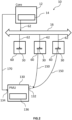
- Fig.1 represents schematically an example embodiment of a semiconductor device 10 according to the invention.
- power consumption by an electronic circuit increases with the frequency of the clock used by the circuit, and with the square of the voltage applied to the circuit. Therefore, it is known to vary (reduce) the frequency of the clock, and the voltage of the power applied to a circuit.
- the semiconductor device 10 according to the invention is subdivided in different parts, which comprise:
- the semiconductor device may be operated according to different operating modes, such as Active, Run, Sleep, DeepSleep, Standby, Stop, Idle, Off, Shutdown.
- the operating modes may comprise, e.g.,
- the software application 14 may interact with the peripherals for setting the peripheral in a particular selected configuration by sending a peripheral configuration signal 62.
- the peripheral configuration may comprise operational on or off state, a particular clock frequency to be used, or to select no clock, or to select a particular voltage, or to select no voltage at all.
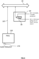
- the software applications may decide to issue a sleep request 170.
- the sleep request 170 is part of the instruction set.
- the sleep request 170 may be transmitted by the core 12 to the PMU 130.
- the PMU 130 obtains the value of the configuration of the peripherals.
- An input port 132 is provided at the PMU 130 for receiving the values of the configuration of the peripherals 60.
- the PMU 130 comprises a control logic module 136 for receiving the values of the configurations and, upon receiving a sleep request, to determine the target operating mode to select for the semiconductor device 10 in dependence of the configurations of the peripherals 60.
- Fig.2 represents schematically parts of an example embodiment of a semiconductor device 10 according to the invention.
- the peripherals 60 may comprise a Peripheral Control and Status Register (PCSR) 30, each having a number of bits enabling to control the peripheral, e.g. activating or deactivating the peripheral, or specifying the clock to be used for clocking the peripheral, or representing the status of the peripheral.
- the device 10 may comprise a first bus 16.
- the PCSRs may then be accessed in write mode through the first bus 16, e.g. by the core running an application program and deciding to enable or disable one or more of the peripherals, and to select a fast or a slow clock based on the needs of the application.
- the peripheral configuration signal 62 may then be sent through the first bus 16.
- the PMU 130 may obtain access of the values stored in the PCSR's through a set of wires 150 linking directly the PCSRs and the input port 132 of the PMU. These wires 150 may lead the contents of the bits of the PCSR's or a logical function thereof to the PMU 130. For the sake of clarity, these wires are not represented on Fig.1 , but symbolized as arrow 150.
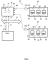
- Fig.3 represents schematically parts of an example embodiment of a semiconductor device 10 according to the invention.
- the components 18 comprise a clock generator module 100 comprising one or more clock generators 105, configured for providing one or more clocks to the peripherals 60, a wire linking the clock output terminals 110 of the clock generator module 100 to the clock input terminals 50 of the peripherals.
- a single line is represented on Fig.3 , a plurality of wires may be provided, according to the numbers of clocks produced by the clock generator module 100, the symbol "//" representing that a plurality of wires may be present, the clock input terminals having then the same number of contact points.
- the PMU 130 When the PMU 130 receives a sleep request and obtains the value of the configuration of the peripherals, the PMU selects an operating mode for the semiconductor device, and sends first commands 107 to the clock generator module 100, for setting the clock generators 105 according to the selected operating mode, e.g. in on or off state, or at a specified frequency.
- the PMU 130 may be configured for sending the first commands 107 directly through one or more wires.
- a wire may be provided for switching a clock generator 105 "on" of "off”.
- the semiconductor device may also comprise a second bus 17 for exchanging data between the PMU and the components 18.
- the second bus 17 may be a dedicated bus or may be the first bus 16.
- the PMU 130 may then be configured for sending the first commands 107 directly through said second bus 17.
- the first commands may comprise a sequence of operations for safely transiting the semiconductor device 10 from one operating mode to another operating mode, e.g. providing periods for oscillators to settle, for voltage regulators to settle, for saving data, or generally for giving circuits a period of time for adapting to the new conditions.
- Fig.4 represents schematically parts of an example embodiment of a semiconductor device 10 according to the invention.
- the components 18 comprise a Voltage Generator Module 70 comprising one or more voltage generators 75.
- the semiconductor device comprises one or more power domains 20, 20'.
- a power domain may group one or more peripherals 60.
- a wire is provided for linking the voltage output terminals 80 of the VGM 70 to the voltage input terminals 40 of the power domains 20, 20', for receiving a voltage for powering the peripheral(s) 60 comprised in the power domain.
- Each power domain may be provided with a clock input terminal 50, for receiving one or more clock for clocking the peripheral(s) comprised in the power domain, as described above.
- the device may comprise any number of power domains, each having any number of peripherals 60, as suitable for the needs of the application.
- the PMU 130 when the PMU 130 receives a sleep request and obtains the value of the configuration of the peripherals, the PMU selects an operating mode for the semiconductor device, and sends a second command 77 to the voltage generator module 70, for setting the voltage generators 75 according to the selected operating mode, e.g. in 'on' or 'off' state, or at a specified voltage.
- the PMU 130 may be configured for sending the second commands 77 directly through one or more wires.
- the semiconductor device may comprise a second bus 17 for exchanging data between the PMU and the components 18.
- the second bus 17 may be a dedicated bus or may be the first bus 16.
- the PMU 130 may then be configured for sending the second commands 77 directly through said second bus 17.
- the second commands 77 may also comprise a sequence of operations.
- the device according to the embodiment of Fig.4 may additionally comprise a power gating switch 140, for at least one of the power domains 20, 20', for enabling power supply to the power domain when in the "on” state, and for insulating the power domain from the VGM 70 when in the "off” state.
- the PMU 130 may, upon receiving said sleep request, determine the state to be set to the power gating switches 140 in dependence of the configuration of the peripherals, control the power gating switch by sending third commands, for configuring the semiconductor device in an operating mode dependent on the configurations of the peripherals.
- Fig.5 represents schematically a detailed view of a peripheral 60 in a device according to the invention.
- the plurality of clocks comprises two clocks, a slow clock, and a fast clock.
- the peripheral 60 comprises a PCSR 30 having three bits. Bit 0 is dedicated to control the state of the peripheral, being disabled when equal to 0 and enabled when equal to 1.
- the bits 1 and 2 are used for selecting the clock to be used by the peripheral.
- the clock is gated, i.e. no clock is admitted in the peripheral.
- the slow clock is selected, and when equal to 10, the fast clock is selected.
- the 11 combination is not used.
- the application program may decide that a particular peripheral is not needed in the future, and therefore set its enable/disable bit to zero.
- the application program may decide that another peripheral is needed but may run at a lower speed, because the function is not time-critical. Therefore, for saving power, the application program may set the enable bit, and write '01 to bits 1 and 2 for selecting the slow clock.
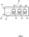
- Fig.6 represents schematically a power domain 20 in an embodiment of the invention, comprising a frequency divider module 65.
- the frequency divider module receives a clock from the clock generator module, and may divide the clock into a plurality of clocks having different frequencies, e.g. divided by 2, 4, 8 or other factors.
- the peripherals 60 may then select one of these divided clocks for clocking the peripheral, depending on the PCSR's 30.
- the control logic module 136 comprised in the PMU is configured for translating the configuration of the peripherals, made by the application program, into a selected one of the operating modes, and for conveying the needed configuration of the voltages and clocks to the VGM 70 and/or to the clock generator module 100 and/or to the other required components 18.
- the PMU may clock gate all the peripherals by shutting off one or more of the clock generators 105, or if power-gating is available, the PMU may set the power gating switch 140 to 'off' if this corresponds to the target mode of operation.
- microcontroller with multiple peripherals for communication purposes such as SPI, I2C, UART, for timing purposes such as timer, RTC, watchdog, for analog sensing purposes such as ADC, comparator, for security purposes such as AES, random number generator.
- the microcontroller is partitioned in three power domains.
- Power domain 1 includes the core of the microcontroller.
- Power domain 2 includes ADC, comparator, SPI, I2C, timer, watchdog, AES and random number generator.
- Power domain 3 includes RTC and UART.
- the microcontroller has two clock generators that generate a high and a low frequency.
- the microcontroller has two voltage generators that generate a high and a low voltage.
- the application program can configure each peripheral to be operated with a high or a low frequency.
- the core is supplied by a low voltage.
- the other peripherals are supplied with a high voltage.
- the microcontroller has four operating modes. Mode 1 has all domains powered and clocked, all clock generators activated and all voltage generators activated. Mode 2 has domain 1 powered but clock gated, domains 2 and 3 powered and clocked, all clock generators activated and all voltage generators activated. Mode 3 has domain 1 and 2 power gated, domain 3 powered and clocked, all clock generators activated and only high voltage generator activated.
- Mode 4 has domain 1 and 2 power gated, domain 3 powered and clocked, only low frequency clock generator activated and only high voltage generator activated.
- the microcontroller is in mode 1. Then, when the user request by software to go to sleep, the PMU will check which functionalities are required. If the SPI is activated (thus required), the PMU will choose mode 2 (because SPI is not available in mode 3 and 4). If only UART is activated and a high frequency is selected, the PMU will choose mode 3 (because high frequency clock generator is still required). If only UART is activated and a low frequency is selected, the PMU will choose mode 4.
- Fig.7 represents a flow diagram of a method of operating a semiconductor device according to the invention.
- the semiconductor device of the invention may be operated as follows:
- the application program only enables or disables the peripherals and selects the clock speed and/or the voltage to be used, according to the needs of the application.
- the task of determining how to configure the device is performed by the PMU, and the burden of deciding the optimal configuration of the operating modes is not on the application program.
Landscapes
- Engineering & Computer Science (AREA)
- Theoretical Computer Science (AREA)
- General Engineering & Computer Science (AREA)
- Physics & Mathematics (AREA)
- General Physics & Mathematics (AREA)
- Computer Hardware Design (AREA)
- Computing Systems (AREA)
- Power Sources (AREA)
- Microcomputers (AREA)
- Semiconductor Integrated Circuits (AREA)
Priority Applications (7)
| Application Number | Priority Date | Filing Date | Title |
|---|---|---|---|
| EP22162896.9A EP4246285A1 (fr) | 2022-03-18 | 2022-03-18 | Gestion de modes de fonctionnement de dispositifs semi-conducteurs |
| TW112105554A TW202339400A (zh) | 2022-03-18 | 2023-02-16 | 半導體器件及操作半導體器件的方法 |
| CN202380026121.0A CN118829959A (zh) | 2022-03-18 | 2023-03-07 | 半导体器件操作模式管理 |
| US18/847,334 US20250208690A1 (en) | 2022-03-18 | 2023-03-07 | Semiconductor device operating modes management |
| PCT/EP2023/055747 WO2023174756A1 (fr) | 2022-03-18 | 2023-03-07 | Gestion de modes de fonctionnement de dispositif à semi-conducteur |
| JP2024554812A JP2025509578A (ja) | 2022-03-18 | 2023-03-07 | 半導体デバイスの動作モード管理 |
| KR1020247032160A KR20240165956A (ko) | 2022-03-18 | 2023-03-07 | 반도체 디바이스 동작 모드 관리 |
Applications Claiming Priority (1)
| Application Number | Priority Date | Filing Date | Title |
|---|---|---|---|
| EP22162896.9A EP4246285A1 (fr) | 2022-03-18 | 2022-03-18 | Gestion de modes de fonctionnement de dispositifs semi-conducteurs |
Publications (1)
| Publication Number | Publication Date |
|---|---|
| EP4246285A1 true EP4246285A1 (fr) | 2023-09-20 |
Family
ID=80819839
Family Applications (1)
| Application Number | Title | Priority Date | Filing Date |
|---|---|---|---|
| EP22162896.9A Pending EP4246285A1 (fr) | 2022-03-18 | 2022-03-18 | Gestion de modes de fonctionnement de dispositifs semi-conducteurs |
Country Status (7)
| Country | Link |
|---|---|
| US (1) | US20250208690A1 (fr) |
| EP (1) | EP4246285A1 (fr) |
| JP (1) | JP2025509578A (fr) |
| KR (1) | KR20240165956A (fr) |
| CN (1) | CN118829959A (fr) |
| TW (1) | TW202339400A (fr) |
| WO (1) | WO2023174756A1 (fr) |
Citations (4)
| Publication number | Priority date | Publication date | Assignee | Title |
|---|---|---|---|---|
| US20090089599A1 (en) | 2007-10-01 | 2009-04-02 | Silicon Laboratories Inc. | Power supply system for low power mcu |
| US20140122908A1 (en) * | 2010-04-07 | 2014-05-01 | Apple Inc. | Hardware Automatic Performance State Transitions in System on Processor Sleep and Wake Events |
| US8975916B1 (en) | 2009-08-28 | 2015-03-10 | Cypress Semiconductor Corporation | Self-modulated voltage reference |
| US20190079573A1 (en) * | 2017-09-12 | 2019-03-14 | Ambiq Micro, Inc. | Very Low Power Microcontroller System |
Family Cites Families (3)
| Publication number | Priority date | Publication date | Assignee | Title |
|---|---|---|---|---|
| EP0708406B1 (fr) * | 1994-10-19 | 2001-09-12 | Advanced Micro Devices, Inc. | Systèmes processeurs intégrés pour dispositifs d'information portables |
| WO2013176449A1 (fr) * | 2012-05-21 | 2013-11-28 | 엘지전자 주식회사 | Dispositif de puissance, dispositif de commande de puissance et procédé d'exploitation associé |
| US20150067363A1 (en) * | 2013-09-04 | 2015-03-05 | Sebastien Jouin | Clock generator circuit with automatic sleep mode |
-
2022
- 2022-03-18 EP EP22162896.9A patent/EP4246285A1/fr active Pending
-
2023
- 2023-02-16 TW TW112105554A patent/TW202339400A/zh unknown
- 2023-03-07 WO PCT/EP2023/055747 patent/WO2023174756A1/fr not_active Ceased
- 2023-03-07 CN CN202380026121.0A patent/CN118829959A/zh active Pending
- 2023-03-07 KR KR1020247032160A patent/KR20240165956A/ko active Pending
- 2023-03-07 JP JP2024554812A patent/JP2025509578A/ja active Pending
- 2023-03-07 US US18/847,334 patent/US20250208690A1/en active Pending
Patent Citations (4)
| Publication number | Priority date | Publication date | Assignee | Title |
|---|---|---|---|---|
| US20090089599A1 (en) | 2007-10-01 | 2009-04-02 | Silicon Laboratories Inc. | Power supply system for low power mcu |
| US8975916B1 (en) | 2009-08-28 | 2015-03-10 | Cypress Semiconductor Corporation | Self-modulated voltage reference |
| US20140122908A1 (en) * | 2010-04-07 | 2014-05-01 | Apple Inc. | Hardware Automatic Performance State Transitions in System on Processor Sleep and Wake Events |
| US20190079573A1 (en) * | 2017-09-12 | 2019-03-14 | Ambiq Micro, Inc. | Very Low Power Microcontroller System |
Also Published As
| Publication number | Publication date |
|---|---|
| KR20240165956A (ko) | 2024-11-25 |
| CN118829959A (zh) | 2024-10-22 |
| US20250208690A1 (en) | 2025-06-26 |
| JP2025509578A (ja) | 2025-04-11 |
| TW202339400A (zh) | 2023-10-01 |
| WO2023174756A1 (fr) | 2023-09-21 |
Similar Documents
| Publication | Publication Date | Title |
|---|---|---|
| US10585448B2 (en) | Low power autonomous peripheral management | |
| CN1549961B (zh) | 动态电压控制方法与设备 | |
| CN1202457C (zh) | 处理器控制电压的系统中提供决定开启电压的方法及装置 | |
| CN100426177C (zh) | 在集成电路上的电子系统中动态控制功率的系统和方法 | |
| US20050144492A1 (en) | Processor system and method for reducing power consumption in idle mode | |
| US20010007113A1 (en) | Power management circuit that qualifies powergood disable signal | |
| US20050215227A1 (en) | Method and apparatus for entering a low power mode | |
| EP2626757A1 (fr) | Machine en état fini pour système de gestion | |
| US10732697B2 (en) | Voltage rail coupling sequencing based on upstream voltage rail coupling status | |
| US11119559B2 (en) | Controlling a processor clock | |
| US11755096B2 (en) | Method and apparatus for selectable high performance or low power processor system | |
| JPH08234864A (ja) | 半導体集積回路 | |
| US20100325451A1 (en) | Power-saving trigger-type control device for dynamically and instantly varying frequency and method thereof | |
| CN102929381B (zh) | 电子系统及其电源管理方法 | |
| US9841804B2 (en) | Clocking a processor | |
| WO2019094108A1 (fr) | Commande d'horloge dynamique pour augmenter l'efficacité dans un sous-système de mémoire | |
| EP4246285A1 (fr) | Gestion de modes de fonctionnement de dispositifs semi-conducteurs | |
| CN120122799A (zh) | 一种基于ASPM的PCIe加密卡低功耗实现方法及系统 | |
| US20240329707A1 (en) | Power management for multiple circuit domains | |
| KR100706224B1 (ko) | 컴퓨터 시스템의 웨이크 업 방법 | |
| JP2025509578A5 (fr) | ||
| CN118363445A (zh) | 微控制电路及管理方法 | |
| CN110362187A (zh) | 用于功率管理的系统和方法 | |
| JP2004094930A (ja) | 半導体集積回路 | |
| JPH04239305A (ja) | 情報処理装置 |
Legal Events
| Date | Code | Title | Description |
|---|---|---|---|
| PUAI | Public reference made under article 153(3) epc to a published international application that has entered the european phase |
Free format text: ORIGINAL CODE: 0009012 |
|
| STAA | Information on the status of an ep patent application or granted ep patent |
Free format text: STATUS: THE APPLICATION HAS BEEN PUBLISHED |
|
| AK | Designated contracting states |
Kind code of ref document: A1 Designated state(s): AL AT BE BG CH CY CZ DE DK EE ES FI FR GB GR HR HU IE IS IT LI LT LU LV MC MK MT NL NO PL PT RO RS SE SI SK SM TR |
|
| STAA | Information on the status of an ep patent application or granted ep patent |
Free format text: STATUS: REQUEST FOR EXAMINATION WAS MADE |
|
| 17P | Request for examination filed |
Effective date: 20240320 |
|
| RBV | Designated contracting states (corrected) |
Designated state(s): AL AT BE BG CH CY CZ DE DK EE ES FI FR GB GR HR HU IE IS IT LI LT LU LV MC MK MT NL NO PL PT RO RS SE SI SK SM TR |
|
| STAA | Information on the status of an ep patent application or granted ep patent |
Free format text: STATUS: EXAMINATION IS IN PROGRESS |
|
| 17Q | First examination report despatched |
Effective date: 20250724 |