EP4246728A1 - Structures d'antenne pour dispositifs de combinaison de puissance spatiale - Google Patents
Structures d'antenne pour dispositifs de combinaison de puissance spatiale Download PDFInfo
- Publication number
- EP4246728A1 EP4246728A1 EP23158619.9A EP23158619A EP4246728A1 EP 4246728 A1 EP4246728 A1 EP 4246728A1 EP 23158619 A EP23158619 A EP 23158619A EP 4246728 A1 EP4246728 A1 EP 4246728A1
- Authority
- EP
- European Patent Office
- Prior art keywords
- amplifier
- antenna structure
- conductor
- output
- input
- Prior art date
- Legal status (The legal status is an assumption and is not a legal conclusion. Google has not performed a legal analysis and makes no representation as to the accuracy of the status listed.)
- Pending
Links
Images


Classifications
-
- H—ELECTRICITY
- H01—ELECTRIC ELEMENTS
- H01P—WAVEGUIDES; RESONATORS, LINES, OR OTHER DEVICES OF THE WAVEGUIDE TYPE
- H01P5/00—Coupling devices of the waveguide type
- H01P5/12—Coupling devices having more than two ports
- H01P5/16—Conjugate devices, i.e. devices having at least one port decoupled from one other port
-
- H—ELECTRICITY
- H01—ELECTRIC ELEMENTS
- H01Q—ANTENNAS, i.e. RADIO AERIALS
- H01Q23/00—Antennas with active circuits or circuit elements integrated within them or attached to them
-
- H—ELECTRICITY
- H01—ELECTRIC ELEMENTS
- H01P—WAVEGUIDES; RESONATORS, LINES, OR OTHER DEVICES OF THE WAVEGUIDE TYPE
- H01P3/00—Waveguides; Transmission lines of the waveguide type
- H01P3/02—Waveguides; Transmission lines of the waveguide type with two longitudinal conductors
- H01P3/06—Coaxial lines
-
- H—ELECTRICITY
- H01—ELECTRIC ELEMENTS
- H01P—WAVEGUIDES; RESONATORS, LINES, OR OTHER DEVICES OF THE WAVEGUIDE TYPE
- H01P5/00—Coupling devices of the waveguide type
- H01P5/12—Coupling devices having more than two ports
-
- H—ELECTRICITY
- H01—ELECTRIC ELEMENTS
- H01Q—ANTENNAS, i.e. RADIO AERIALS
- H01Q13/00—Waveguide horns or mouths; Slot antennas; Leaky-waveguide antennas; Equivalent structures causing radiation along the transmission path of a guided wave
- H01Q13/08—Radiating ends of two-conductor microwave transmission lines, e.g. of coaxial lines, of microstrip lines
- H01Q13/085—Slot-line radiating ends
-
- H—ELECTRICITY
- H01—ELECTRIC ELEMENTS
- H01Q—ANTENNAS, i.e. RADIO AERIALS
- H01Q25/00—Antennas or antenna systems providing at least two radiating patterns
- H01Q25/005—Antennas or antenna systems providing at least two radiating patterns providing two patterns of opposite direction; back to back antennas
-
- H—ELECTRICITY
- H03—ELECTRONIC CIRCUITRY
- H03F—AMPLIFIERS
- H03F3/00—Amplifiers with only discharge tubes or only semiconductor devices as amplifying elements
- H03F3/189—High-frequency amplifiers, e.g. radio frequency amplifiers
- H03F3/19—High-frequency amplifiers, e.g. radio frequency amplifiers with semiconductor devices only
-
- H—ELECTRICITY
- H03—ELECTRONIC CIRCUITRY
- H03F—AMPLIFIERS
- H03F3/00—Amplifiers with only discharge tubes or only semiconductor devices as amplifying elements
- H03F3/189—High-frequency amplifiers, e.g. radio frequency amplifiers
- H03F3/19—High-frequency amplifiers, e.g. radio frequency amplifiers with semiconductor devices only
- H03F3/195—High-frequency amplifiers, e.g. radio frequency amplifiers with semiconductor devices only in integrated circuits
-
- H—ELECTRICITY
- H03—ELECTRONIC CIRCUITRY
- H03F—AMPLIFIERS
- H03F3/00—Amplifiers with only discharge tubes or only semiconductor devices as amplifying elements
- H03F3/20—Power amplifiers, e.g. Class B amplifiers, Class C amplifiers
- H03F3/24—Power amplifiers, e.g. Class B amplifiers, Class C amplifiers of transmitter output stages
- H03F3/245—Power amplifiers, e.g. Class B amplifiers, Class C amplifiers of transmitter output stages with semiconductor devices only
Definitions
- the disclosure relates generally to power-combining devices and, more particularly, to antenna structures for spatial power-combining devices.
- Solid state power amplifiers are used for broadband radio frequency power amplification in commercial and defense communications, radar, electronic warfare, satellite, and various other communication systems. As modern SSPA applications continue to advance, increasingly higher and higher saturated output power is desired. While millimeter wave (mmWave) gallium nitride (GaN) monolithic microwave integrated circuits (MMICs) have made great strides for use in SSPAs, there are many applications where even higher power densities may be out of reach for a single device. Spatial power-combining devices have been developed that provide a means to combine the output of several separate MMICs to realize a SSPA with much larger output power than that of a single device. Spatial power-combining techniques are implemented by combining broadband signals from a number of amplifiers to provide output powers with high efficiencies and operating frequencies.
- mmWave gallium nitride
- MMICs monolithic microwave integrated circuits
- One example of a spatial power-combining device utilizes a plurality of solid-state amplifier assemblies that forms a coaxial waveguide to amplify an electromagnetic signal.
- Each amplifier assembly may include an input antenna structure, an amplifier, and an output antenna structure.
- the input antenna structures may form an input antipodal antenna array
- the output antenna structures may form an output antipodal antenna array.
- an electromagnetic signal is passed through an input port to an input coaxial waveguide section of the spatial power-combining device.
- the input coaxial waveguide section distributes the electromagnetic signal to be split across the input antipodal antenna array.
- the amplifiers receive the split signals and in turn transmit amplified split signals across the output antipodal antenna array.
- the output antipodal antenna array and an output coaxial waveguide section combine the amplified split signals to form an amplified electromagnetic signal that is passed to an output port of the spatial power-combining device.
- Antenna structures for spatial power-combining devices typically include an antenna signal conductor and an antenna ground conductor deposited on opposite sides of a substrate, such as a printed circuit board.
- the size of the antenna structures is related to an operating frequency of the spatial power-combining device.
- the size of the input antenna structure is related to the frequency of energy that can be efficiently received
- the size of the output antenna structure is related to the frequency of energy that can be efficiently transmitted.
- Overall sizes of spatial power-combining devices typically scale larger or smaller depending on desired operating frequency ranges.
- Spatial power-combining devices include amplifier assemblies with amplifiers and antenna structures supported by body structures.
- Body structures may include inner surfaces that are closer to a center axis of the spatial power-combining device where the inner surfaces have peripheral edges that are inset from remainders of the body structures.
- Antenna structures are disclosed that are arranged within inset portions such that the antenna structures are bounded on one end by the body structures.
- a portion of a coaxial waveguide section that engages with the amplifier assemblies may bound opposing ends of the antenna structures.
- a spatial power-combining device comprises a plurality of amplifier assemblies, each amplifier assembly of the plurality of amplifier assemblies comprising: a body structure comprising a first face, a second face that is on an opposite side of the body structure than the first face, and an outer surface and an inner surface that are arranged between the first face and the second face; an amplifier arranged on the first face of the body structure; and an antenna structure coupled to the amplifier, wherein the antenna structure is positioned outside a peripheral edge of the inner surface.
- the antenna structure comprises a signal conductor on a first side of a substrate and a ground conductor on a second side of the substrate that is opposite the first side, wherein the signal conductor and the ground conductor are positioned outside the peripheral edge of the body structure at the inner surface.
- the substrate forms a tab that protrudes from the body structure, and the signal conductor and the ground conductor are positioned on the tab.
- the amplifier comprises a monolithic microwave integrated circuit (MMIC) amplifier.
- the plurality of amplifier assemblies are radially arranged around a center axis.
- each amplifier assembly of the plurality of amplifier assemblies forms a wedge shape, and the plurality of amplifier assemblies are radially arranged to form a center waveguide section.
- the antenna structure is an output antenna structure
- the peripheral edge is a first peripheral edge of the inner surface
- each amplifier assembly of the plurality of amplifier assemblies further comprises an input antenna structure positioned outside a second peripheral edge of the inner surface.
- the spatial power-combining device may further comprise: an input coaxial waveguide section configured to concurrently provide a signal to the input antenna structure of each amplifier assembly of the plurality of amplifier assemblies; and an output coaxial waveguide section configured to concurrently combine a signal from the output antenna structure of each amplifier assembly of the plurality of amplifier assemblies.
- a spatial power-combining device comprises: a coaxial waveguide section comprising an inner conductor and an outer conductor; and a plurality of amplifier assemblies, each amplifier assembly of the plurality of amplifier assemblies comprising: a body structure comprising a first face, a second face that is on an opposite side of the body structure than the first face, and an outer surface and an inner surface that are arranged between the first face and the second face; an amplifier arranged on the first face of the body structure; and an antenna structure coupled to the amplifier, the antenna structure being arranged between the inner conductor and the body structure.
- the antenna structure is positioned outside a peripheral edge of the inner surface of the body structure.
- the antenna structure comprises a signal conductor on a first side of a substrate and a ground conductor on a second side of the substrate that is opposite the first side, wherein the signal conductor and the ground conductor are positioned outside a peripheral edge of the inner surface of the body structure.
- the antenna structure is an output antenna structure, the inner conductor is an output inner conductor, and the outer conductor is an output outer conductor; the coaxial waveguide section is an output coaxial waveguide section; and each amplifier assembly of the plurality of amplifier assemblies further comprises an input antenna structure.
- the spatial power-combining device may further comprise an input coaxial waveguide section comprising an input inner conductor and an input outer conductor, wherein the input antenna structure is arranged between the input inner conductor and the body structure.
- an amplifier assembly comprises: a body structure comprising a first face, a second face that is on an opposite side of the body structure than the first face, and an outer surface and an inner surface that are arranged between the first face and the second face, wherein a length of the inner surface along the first face is less than a length of the outer surface along the first face; an amplifier arranged on the first face of the body structure; and an antenna structure coupled to the amplifier.
- the antenna structure is positioned outside a peripheral edge of the inner surface of the body structure.
- the antenna structure is an output antenna structure, the peripheral edge is a first peripheral edge of the inner surface, and the amplifier assembly further comprises an input antenna structure positioned outside a second peripheral edge of the inner surface.
- the input antenna structure and the output antenna structure are formed on a substrate; the substrate forms a first tab that protrudes from the body structure and the input antenna structure is positioned on the first tab; and the substrate forms a second tab that protrudes from the body structure and the output antenna structure is positioned on the second tab.
- the amplifier comprises a MMIC amplifier.
- the amplifier assembly forms a wedge shape.
- the outer surface is an arcuate outer surface configured to form a portion of a cylindrical shape.
- any of the foregoing aspects individually or together, and/or various separate aspects and features as described herein, may be combined for additional advantage. Any of the various features and elements as disclosed herein may be combined with one or more other disclosed features and elements unless indicated to the contrary herein.
- Embodiments are described herein with reference to schematic illustrations of embodiments of the disclosure. As such, the actual dimensions of the layers and elements can be different, and variations from the shapes of the illustrations as a result, for example, of manufacturing techniques and/or tolerances, are expected. For example, a region illustrated or described as square or rectangular can have rounded or curved features, and regions shown as straight lines may have some irregularity. Thus, the regions illustrated in the figures are schematic and their shapes are not intended to illustrate the precise shape of a region of a device and are not intended to limit the scope of the disclosure. Additionally, sizes of structures or regions may be exaggerated relative to other structures or regions for illustrative purposes and, thus, are provided to illustrate the general structures of the present subject matter and may or may not be drawn to scale. Common elements between figures may be shown herein with common element numbers and may not be subsequently re-described.
- Spatial power-combining devices include amplifier assemblies with amplifiers and antenna structures supported by body structures.
- Body structures may include inner surfaces that are closer to a center axis of the spatial power-combining device where the inner surfaces have peripheral edges that are inset from remainders of the body structures.
- Antenna structures are disclosed that are arranged within inset portions such that the antenna structures are bounded on one end by the body structures.
- a portion of a coaxial waveguide section that engages with the amplifier assemblies may bound opposing ends of the antenna structures.
- the embodiments are particularly adapted to spatial power-combining devices that operate at microwave frequencies, such as, by way of a non-limiting example, energy between about 300 megahertz (MHz) (100 centimeters (cm) wavelength) and 300 gigahertz (GHz) (0.1 cm wavelength). Additionally, embodiments may comprise operating frequency ranges that extend above microwave frequencies. In some embodiments, by way of non-limiting examples, the operating frequency range includes an operating bandwidth of 4 GHz to 40 GHz, or 2 GHz to 18 GHz, or 2 GHz to 20 GHz, or 20 to 40 GHz, or 25 to 40 GHz, among others.
- a spatial power-combining device typically includes a plurality of amplifier assemblies, and each amplifier assembly typically comprises an individual signal path that includes an amplifier connected to an input antenna structure and an output antenna structure.
- An input coaxial waveguide is configured to provide a signal concurrently to each input antenna structure, and an output coaxial waveguide is configured to concurrently combine amplified signals from each output antenna structure.
- the plurality of amplifier assemblies is arranged coaxially about a center axis. Accordingly, the spatial power-combining device is configured to split, amplify, and combine an electromagnetic signal.
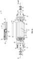
- FIG. 1A is a partially-exploded perspective view of an example spatial power-combining device 10.
- the spatial power-combining device 10 may comprise an input port 12 and an input coaxial waveguide section 14.
- the input coaxial waveguide section 14 provides a broadband transition from the input port 12 to a center waveguide section 16. Electrically, the input coaxial waveguide section 14 provides broadband impedance matching from an impedance Z p1 of the input port 12 to an impedance Z c of the center waveguide section 16.
- the input coaxial waveguide section 14 may include an inner conductor 18 and an outer conductor 20 that radially surrounds the inner conductor 18, thereby forming an opening therebetween. Outer surfaces of the inner conductor 18 and an inner surface of the outer conductor 20 may have gradually changed profiles configured to minimize the impedance mismatch from the input port 12 to the center waveguide section 16.
- the center waveguide section 16 comprises a plurality of amplifier assemblies 22 arranged radially around a center axis of the spatial power-combining device 10.
- a center post 24 is provided at the center axis for mechanical support and the plurality of amplifier assemblies 22 may be positioned circumferentially around the center post 24. In other embodiments, the center post 24 may be omitted.
- FIG. 1A the center post 24 is illustrated in an exploded manner.
- Each amplifier assembly 22 may include a body structure 26 having a predetermined wedge-shaped cross-section, an inner surface 28, and an arcuate outer surface 30. When the amplifier assemblies 22 are collectively assembled radially about the center axis, they form the center waveguide section 16 with a generally cylindrical shape; however, other shapes are possible, such as rectangular, oval, or other geometric shapes.
- the spatial power-combining device 10 may also comprise an output coaxial waveguide section 32 and an output port 34.
- the input port 12 and the output port 34 may comprise any of a field-replaceable Subminiature A (SMA) connector, a super SMA connector, a type N connector, a type K connector, a WR28 connector, other coaxial to waveguide transition connectors, or any other suitable coaxial or waveguide connectors.
- SMA field-replaceable Subminiature A
- the output port 34 may comprise a waveguide output port, such as a WR28 or another sized waveguide.
- the output coaxial waveguide section 32 provides a broadband transition from the center waveguide section 16 to the output port 34.
- the output coaxial waveguide section 32 provides broadband impedance matching from the impedance Z c of the center waveguide section 16 to an impedance Z p2 of the output port 34.
- the output coaxial waveguide section 32 includes an inner conductor 36 and an outer conductor 38 that radially surrounds the inner conductor 36, thereby forming an opening therebetween. Outer surfaces of the inner conductor 36 and an inner surface of the outer conductor 38 may have gradually changed profiles configured to minimize the impedance mismatch from the output port 34 to the center waveguide section 16.
- a pin 40 connects between the input port 12 and the input coaxial waveguide section 14, and a pin 42 connects between the output port 34 and the output coaxial waveguide section 32.
- the center post 24 connects with the inner conductors 18, 36 by way of screws 44, 46 on opposite ends of the center post 24.
- the center post 24 is provided for simplifying mechanical connections, may have other than a cylindrical shape, or may be omitted altogether.
- Each amplifier assembly 22 comprises an input antenna structure 48 and an output antenna structure 50, both of which are coupled to an amplifier 52.
- the amplifier 52 comprises a monolithic microwave integrated circuit (MMIC) amplifier.
- the MMIC may be a solid-state gallium nitride (GaN)-based MMIC.
- GaN MMIC device provides high power density and bandwidth, and a spatial power-combining device may combine power from a plurality of GaN MMICs efficiently in a single step to minimize combining loss.
- an input signal 54 is propagated from the input port 12 to the input coaxial waveguide section 14, where it radiates between the inner conductor 18 and the outer conductor 20 and concurrently provides the input signal 54 to the center waveguide section 16.
- the input antenna structures 48 of the plurality of amplifier assemblies 22 collectively form an input antenna array 56.
- the input antenna array 56 couples the input signal 54 from the input coaxial waveguide section 14, distributing the input signal 54 substantially evenly to each one of the amplifier assemblies 22.
- Each input antenna structure 48 receives a signal portion of the input signal 54 and communicates the signal portion to the amplifier 52.
- the amplifier 52 amplifies the signal portion of the input signal 54 to generate an amplified signal portion that is then transmitted from the amplifier 52 to the output antenna structure 50.
- the output antenna structures 50 collectively form an output antenna array 62 that operates to provide the amplified signal portions to be concurrently combined inside the opening of the output coaxial waveguide section 32 to form an amplified output signal 54 AMP , which is then propagated through the output coaxial waveguide section 32 to the output port 34.
- FIG. 1B is a perspective view of an individual amplifier assembly 22 of the spatial power-combining device 10 of FIG. 1A .
- the input antenna structure 48 may comprise an input signal conductor 64 supported on a first face of a substrate 66 or board, and the output antenna structure 50 comprises an output signal conductor 68 that is also supported on the first face of the substrate 66.
- the input signal conductor 64 and the output signal conductor 68 are electromagnetically coupled to the amplifier 52.
- the substrate 66 may comprise a printed circuit board that provides a desired form factor and mechanical support for the input signal conductor 64 and the output signal conductor 68.
- the input antenna structure 48 also includes an input ground conductor (not visible) on an opposing second face of the substrate 66 to the input signal conductor 64.
- the output antenna structure 50 includes an output ground conductor (not visible) on the opposing second face of the substrate 66 to the output signal conductor 68.
- the substrate 66 may be substituted with a plurality of substrates or boards.
- the input signal conductor 64, the input ground conductor (not visible), the output signal conductor 68, and the output ground conductor (not visible) are mechanically supported by the body structure 26 such that the substrate 66 may not be present.
- one or more ports 70 are provided for an external voltage input, such as from a direct current voltage source, and corresponding bias circuitry 72 is provided to control the amplifier 52.
- the bias circuitry 72 is arranged on the same substrate 66 as the antenna structures 48, 50. In other embodiments, a separate substrate may be provided for the bias circuitry 72.
- a portion of the input signal (54 in FIG. 1A ) is received by the input antenna structure 48 where it radiates between the input signal conductor 64 and the input ground conductor (not visible) and propagates to the amplifier 52 for amplification.
- the portion of the input signal (54 in FIG. 1A ) radiates between the input signal conductor 64 and the input ground conductor (not visible) through the substrate 66.
- the portion of the input signal (54 in FIG. 1A ) radiates between the input signal conductor 64 and the input ground conductor (not visible) through air.
- the amplifier 52 outputs a portion of the amplified signal (54 AMP in FIG. 1A ) to the output antenna structure 50 where it radiates between the output signal conductor 68 and the output ground conductor (not visible) in a similar manner.
- the spatial power-combining device 10 is typically utilized for high power-combining applications.
- the amplifier 52 in each of the amplifier assemblies 22 is configured for high power amplification and may therefore generate a high amount of heat. If the operating temperature of each amplifier 52 increases too much, the performance and lifetime of each amplifier 52 may suffer.
- the plurality of amplifier assemblies 22 forms the center waveguide section 16. In this regard, thermal management may be appropriate to effectively dissipate heat in and around the center waveguide section 16.
- the body structure 26 of each amplifier assembly 22 may typically comprise a thermally conductive material, such as copper (Cu), aluminum (Al), or alloys thereof that are configured to dissipate enough heat from the amplifier 52 to maintain a suitably low operating temperature.
- the body structure 26 may comprise graphite with an electrically conductive film, such as nickel (Ni), Cu, or combinations thereof.
- the body structure 26 may comprise metal-ceramic composites, including copper-diamond and/or aluminum-diamond.
- FIG. 2 is a view of a portion of an amplifier assembly 74 that is similar to the amplifier assembly 22 of FIG. 1B and illustrates an arrangement between the output antenna structure 50 and the body structure 26. While only the output end of the amplifier assembly 74 is shown, it is understood that the opposing input end would have a similar structure.
- the amplifier 52 is connected to the output antenna structure 50 by way of a microstrip feed line 76.
- the microstrip feed line 76 may be formed by metallization that is patterned on the first face of the substrate 66.
- the view provided is from the perspective of the first face of the substrate 66 and an opposing second face of the substrate 66 is positioned between the first face and the body structure 26.
- the substrate 66 is represented as semitransparent to illustrate a position of the output ground conductor 78 of the output antenna structure 50 that is on the second face of the substrate 66.
- One or more electromagnetic interference filters 80 are supported on both the first and second faces of the substrate 66 proximate the output signal conductor 68 and the output ground conductor 78 to help suppress modes and reduce leakage between the amplifier assemblies 22.
- Certain ones of the electromagnetic interference filters 80 on the second face of the substrate 66 may ground the input signal conductor 68 and output ground conductor 78 to the body structure 26.
- Other electromagnetic interference filters 80 on the first face of the substrate 66 may ground the input signal conductor 68 and output ground conductor 78 to a body structure of a neighboring amplifier assembly in a fully-assembled spatial power combining device.
- the microstrip feed line 76 feeds into the output signal conductor 68 that is positioned, along with the output ground conductor 78, in an opening of the body structure 26.
- the output antenna structure 50 is positioned within the opening of the body structure 26.
- inner and outer diameters of the opening correspond with a coaxial waveguide channel formed in an assembled spatial power-combining device.
- the coaxial waveguide channel is configured to propagate electromagnetic signals to and from the amplifier assemblies.
- the opening is bounded by a protrusion 82 or finger of the body structure 26 that protrudes along the inner surface 28.
- an inner surface 82' of the protrusion 82 defines a portion of an inner conductor of the coaxial waveguide channel along with the inner conductor (36 of FIG. 1A ).
- An inner surface 26' of the body structure 26 that is opposite the inner surface 82' of the protrusion 82 bounds the other side of the output antenna structure 50 and the corresponding opening defines a portion of an outer conductor of the coaxial waveguide channel along with the outer conductor (38 of FIG. 1A ). While this structure is sufficient in many spatial power-combining applications, it does place a practical limitation on the overall size of a spatial power-combining device.
- the protrusion 82 can only be so small before mechanical stability may be compromised.
- the cross section of the protrusion 82 must scale inversely with the upper operating frequency.
- the cross section of any single protrusion 82 is at most 1/Nth of the total area. Therefore, an upper limit to both the operating frequency range and output power may be limited primarily by how small the protrusion 82 can be constructed.
- the protrusion 82 of the body structure 26 increases difficulty and costs for repeatable manufacturing as the protrusion 82 requires precision machining. For certain operating frequencies, the protrusion 82 may not be mechanically sound until secured within a fully assembled spatial power-combining device, thereby introducing handling related yield loss.
- amplifier assemblies for spatial power-combining devices include body structures that only define portions of an outer conductor of the coaxial waveguide channel. In this manner, the protrusions along the inner surface as described above may be avoided.
- the inner surface of the body structure is formed inset from the remainder of the body structure and the antenna structures may be positioned proximate inset portions and outside peripheral edges of the body structure at the inner surface.
- the inner conductor of the coaxial waveguide sections may engage with the inset inner surface of the body structure, thereby bounding the antenna structures. Accordingly, the inner conductor of the coaxial waveguide sections forms a beginning portion of the inner conductor of the coaxial waveguide channel that is outside the body structure. In this manner, the scaling of amplifier assemblies for various operating frequencies may not be limited by the presence of the previously described protrusions.
- FIG. 3 is an exploded view of a portion of a spatial power-combining device 84 that includes amplifier assemblies 86 with body structures 26 that only define portions of an outer conductor of the coaxial waveguide channel. While only the output end of the amplifier assembly 86 is shown, it is understood that the arrangements described herein would be equally applicable to the opposing input end and, in many embodiments, the opposing input end would have an identical structure that mirrors the output end. In this regard, the following description relative to the output end may be applied to the input end of the amplifier assembly 86 by replacing the term "output" with "input.”
- FIG. 3 a portion of a single amplifier assembly 86 is illustrated relative to an inner conductor 36 of an output coaxial waveguide section (e.g., 32 of FIG. 1A ).
- FIG. 3 further illustrates an exploded portion of the amplifier assembly 86 that shows the arrangement of the output antenna structure 50 relative to the body structure 26.
- the inner surface 26' of the body structure 26 defines a portion of an outer conductor of the coaxial waveguide channel in a similar manner as described above for FIG. 2 .
- the inner surface 28 of the amplifier assembly 86 is inset from the remainder of the body structure 26 such that a peripheral edge 28' of the inner surface 28 is inset from a peripheral edge 26" of the remainder of the body structure 26.
- the output antenna structure 50 may be positioned outside a peripheral edge 28' of the inner surface 28 and within the peripheral edge 26" of the remainder of the body structure 26.
- the substrate 66 may include or otherwise form a tab 66' that protrudes from the body structure 26 away from the inner surface 26' and in an offset position from the peripheral edge 28' of the inner surface 28. The remainder of the substrate 66 may extend across and be mechanically supported by the body structure 26.
- the output signal conductor 68 and the output ground conductor 78 are positioned on the tab 66'.
- such an arrangement of the output antenna structure 50 may be referred to as a winged endfire antenna structure.
- the antenna structure 50 may not be directly grounded to the body structure 26, such as by way of the electromagnetic interference filters 80 of FIG. 3 . Rather, certain grounding may occur through paths that trace back to the body structure 26 away from the antenna structure 50. For example, while portions of the output ground conductor 78 are floating off of the body structure 26, the output ground conductor 78 may be grounded to the body structure 26 by way of a metallization path back to the body structure 26.
- the inner surface 26' of the body structure 26 defines a portion of an outer conductor of the coaxial waveguide channel.
- the inner conductor 36 When assembled, the inner conductor 36 will reside in a position that is adjacent or abuts the peripheral edge 28' of the inner surface 28.
- the inner conductor 36 will bound the antenna structure 50 in a position that is opposite the inner surface 26', and accordingly, the inner conductor 36 itself will define portions of the coaxial waveguide channel in which the antenna structure 50 resides.
- the protrusion 82 of the body structure 26 described above for FIG. 2 is omitted for the amplifier assembly 86 of FIG. 3 . In this regard, the size restrictions, yield loss, and manufacturability associated with the protrusion 82 of FIG. 2 may be avoided.
- a spatial power-combining device with sixteen amplifier assemblies may be configured as a thirty-two-way spatial power-combining device by arranging two amplifiers and two sets of input and output antenna structures for each of the sixteen amplifier assemblies. This arrangement may be advantageous for higher frequency embodiments where overall size requirements of the spatial power-combining device may necessitate a relative size of each of the thirty-two amplifier assemblies that is too small to be mechanically sound. Combined with the antenna structures as described for FIG. 3 , such arrangements may provide increased output powers for even smaller sized spatial power-combining devices.
- FIG. 4 is a perspective view of an amplifier assembly 88 for a spatial power-combining device that includes multiple sets of antenna structures as described for FIG. 3 to provide increased output power.
- the body structure 26 of the amplifier assembly 88 includes a first recess 74-1 that is formed on a first face 26A of the body structure 26.
- a first substrate 66-1 that includes a first input antenna structure 48-1 and a first output antenna structure 50-1 is arranged on the first face 26A.
- portions of the first substrate 66-1 outside of the microstrip feed lines 76 are omitted. It is understood that the microstrip feed lines 76 provide inputs and outputs to an amplifier that is on the first face 26A.
- a second substrate 66-2 that includes another amplifier coupled to a second input antenna structure 48-2 and a second output antenna structure 50-2 is arranged on an opposing second face 26B. While not entirely visible, the second substrate 66-2 may reside in a second recess 74-2 formed in the second face 26B.
- each of the input antenna structures 48-1, 48-2 and the output antenna structures 50-1, 50-2 are positioned outside peripheral edges of the inner surface 28 while still being within peripheral edges 26" of the remainder of the body structure 26. Accordingly, a length 28 L of the inner surface 28 as measured from the input end to the output end is less than a corresponding length 30 L of the outer surface 30.
- FIGS. 5A to 5D illustrate a portion of a spatial power-combining device 90 that includes the amplifier assembly 88 of FIG. 4 .
- many of the elements of the spatial power-combining device 88 are omitted, including one or more portions of the input port 12, the input coaxial waveguide section 14, the center waveguide section 16, the output coaxial waveguide section 32, and the output port 34 as described for FIG. 1A .
- the fully assembled spatial power-combining device 90 may include any of these elements as described for FIG. 1A .
- FIG. 5A is an exploded view illustrating the amplifier assembly 88 relative to the inner conductor 36.
- the inner conductor 36 may form a portion of an output coaxial waveguide section (e.g., 32 of FIG. 1A ).
- a superimposed dashed arrow in FIG. 5A illustrates a direction in which the inner conductor 36 may be coupled with amplifier assembly 88.
- the peripheral edge 28' of the inner surface 28 of the amplifier assembly 88 may include an alignment notch 90 that is arranged to receive a corresponding protruding feature 36' of the inner conductor 36.
- the inner conductor 36 may mechanically engage with the body structure 26 at the peripheral edge 28' of the inner surface 28 when assembled.
- FIG. 5D is an end view of a portion of the spatial power-combining device 90 when sixteen of the amplifier assemblies 88 are radially arranged to form the center waveguide section 16 of FIG. 1A .
- the inner conductor 36 bounds the first and second output antenna structures 50-1, 50-2 of each of the amplifier assemblies 88, thereby arranging thirty-two output antenna structures for sixteen amplifier assemblies 88.
- FIG. 6 is a scattering parameters (S-parameters) plot illustrating a frequency response of a spatial power-combining device based on a simulated model of the spatial power-combining device 90 of FIGS. 5A to 5D .
- the S-parameter magnitude is plotted in decibels (dB) across a GHz frequency range for the spatial power-combining device configured for 20 GHz to 40 GHz operation.
- the insertion loss labeled as Combiner-Split Port Insertion Loss, is an indication of how much power is transferred.
- the insertion loss response is plotted for scattering parameter S(33,1) to represent a single transmission line of the thirty-two transmission lines.
- a 1 to 32 split loss of -15 dB would correspond with a theoretical zero insertion loss where substantially all power from a signal is transferred.
- the model demonstrates suitable insertion loss across the intended 20 - 40 GHz frequency range.
- the return loss labeled as Combiner Port Return Loss, is an indication of how much power is reflected. When the return loss is equal to 0 dB, then substantially all power from a signal is reflected. Accordingly, it is desirable for return loss to be as low as possible, such as below -20 dB across the intended frequency range.
- the model indicates a thirty-two power combiner with sixteen amplifier assemblies demonstrates a suitable percent bandwidth for operation and retains a greater than octave bandwidth frequency response, which meets the current demands for millimeter wave (mmWave) spatial power-combining architectures.
- mmWave millimeter wave
- Spatial power-combining devices include amplifier assemblies with amplifiers and antenna structures supported by body structures.
- Body structures may include inner surfaces that are closer to a center axis of the spatial power-combining device where the inner surfaces have peripheral edges that are inset from remainders of the body structures.
- Antenna structures are disclosed that are arranged within inset portions such that the antenna structures are bounded on one end by the body structures.
- a portion of a coaxial waveguide section that engages with the amplifier assemblies may bound opposing ends of the antenna structures.
- a spatial power-combining device comprising a plurality of amplifier assemblies, each amplifier assembly of the plurality of amplifier assemblies comprising: a body structure comprising a first face, a second face that is on an opposite side of the body structure than the first face, and an outer surface and an inner surface that are arranged between the first face and the second face; an amplifier arranged on the first face of the body structure; and an antenna structure coupled to the amplifier, wherein the antenna structure is positioned outside a peripheral edge of the inner surface.
- the antenna structure comprises a signal conductor on a first side of a substrate and a ground conductor on a second side of the substrate that is opposite the first side, wherein the signal conductor and the ground conductor are positioned outside the peripheral edge of the body structure at the inner surface.
- each amplifier assembly of the plurality of amplifier assemblies forms a wedge shape, and the plurality of amplifier assemblies are radially arranged to form a center waveguide section.
- each amplifier assembly of the plurality of amplifier assemblies further comprises an input antenna structure positioned outside a second peripheral edge of the inner surface.
- Clause 8 The spatial power-combining device of clause 7, further comprising: an input coaxial waveguide section configured to concurrently provide a signal to the input antenna structure of each amplifier assembly of the plurality of amplifier assemblies; and an output coaxial waveguide section configured to concurrently combine a signal from the output antenna structure of each amplifier assembly of the plurality of amplifier assemblies.
- a spatial power-combining device comprising: a coaxial waveguide section comprising an inner conductor and an outer conductor; and a plurality of amplifier assemblies, each amplifier assembly of the plurality of amplifier assemblies comprising: a body structure comprising a first face, a second face that is on an opposite side of the body structure than the first face, and an outer surface and an inner surface that are arranged between the first face and the second face; an amplifier arranged on the first face of the body structure; and an antenna structure coupled to the amplifier, the antenna structure being arranged between the inner conductor and the body structure.
- the antenna structure comprises a signal conductor on a first side of a substrate and a ground conductor on a second side of the substrate that is opposite the first side, wherein the signal conductor and the ground conductor are positioned outside a peripheral edge of the inner surface of the body structure.
- each amplifier assembly of the plurality of amplifier assemblies further comprises an input antenna structure.
- Clause 13 The spatial power-combining device of clause 12, further comprising an input coaxial waveguide section comprising an input inner conductor and an input outer conductor, wherein the input antenna structure is arranged between the input inner conductor and the body structure.
- An amplifier assembly comprising: a body structure comprising a first face, a second face that is on an opposite side of the body structure than the first face, and an outer surface and an inner surface that are arranged between the first face and the second face, wherein a length of the inner surface along the first face is less than a length of the outer surface along the first face; an amplifier arranged on the first face of the body structure; and an antenna structure coupled to the amplifier.
- Clause 15 The amplifier assembly of clause 14, wherein the antenna structure is positioned outside a peripheral edge of the inner surface of the body structure.
- Clause 16 The amplifier assembly of clause 15, wherein the antenna structure is an output antenna structure, the peripheral edge is a first peripheral edge of the inner surface, and the amplifier assembly further comprises an input antenna structure positioned outside a second peripheral edge of the inner surface.
- Clause 17 The amplifier assembly of clause 16, wherein: the input antenna structure and the output antenna structure are formed on a substrate; the substrate forms a first tab that protrudes from the body structure and the input antenna structure is positioned on the first tab; and the substrate forms a second tab that protrudes from the body structure and the output antenna structure is positioned on the second tab.
- Clause 18 The amplifier assembly of any of clauses 14 to 17, wherein the amplifier comprises a monolithic microwave integrated circuit (MMIC) amplifier.
- MMIC monolithic microwave integrated circuit
- Clause 20 The amplifier assembly of clause 19, wherein the outer surface is an arcuate outer surface configured to form a portion of a cylindrical shape.
Landscapes
- Engineering & Computer Science (AREA)
- Power Engineering (AREA)
- Microelectronics & Electronic Packaging (AREA)
- Microwave Amplifiers (AREA)
Applications Claiming Priority (2)
| Application Number | Priority Date | Filing Date | Title |
|---|---|---|---|
| US202263319508P | 2022-03-14 | 2022-03-14 | |
| US18/158,196 US12609434B2 (en) | 2022-03-14 | 2023-01-23 | Antenna structures for spatial power-combining devices |
Publications (1)
| Publication Number | Publication Date |
|---|---|
| EP4246728A1 true EP4246728A1 (fr) | 2023-09-20 |
Family
ID=85382503
Family Applications (1)
| Application Number | Title | Priority Date | Filing Date |
|---|---|---|---|
| EP23158619.9A Pending EP4246728A1 (fr) | 2022-03-14 | 2023-02-24 | Structures d'antenne pour dispositifs de combinaison de puissance spatiale |
Country Status (2)
| Country | Link |
|---|---|
| US (1) | US12609434B2 (fr) |
| EP (1) | EP4246728A1 (fr) |
Families Citing this family (1)
| Publication number | Priority date | Publication date | Assignee | Title |
|---|---|---|---|---|
| US11955687B2 (en) | 2022-01-10 | 2024-04-09 | Qorvo Us, Inc. | Structural arrangements for spatial power-combining devices |
Citations (5)
| Publication number | Priority date | Publication date | Assignee | Title |
|---|---|---|---|---|
| US4424496A (en) * | 1981-10-13 | 1984-01-03 | Raytheon Company | Divider/combiner amplifier |
| US5920240A (en) * | 1996-06-19 | 1999-07-06 | The Regents Of The University Of California | High efficiency broadband coaxial power combiner/splitter with radial slotline cards |
| US20060202777A1 (en) * | 2005-03-08 | 2006-09-14 | Deckman Blythe C | Method and apparatus for increasing performance in a waveguide-based spatial power combiner |
| US20070229186A1 (en) * | 2006-03-31 | 2007-10-04 | Hacker Jonathan B | Compact stabilized full-band power amplifier arrangement |
| US20130127678A1 (en) * | 2011-11-23 | 2013-05-23 | Raytheon Company | Coaxial waveguide antenna |
Family Cites Families (69)
| Publication number | Priority date | Publication date | Assignee | Title |
|---|---|---|---|---|
| US3023382A (en) | 1960-07-15 | 1962-02-27 | Microwave Dev Lab Inc | Inline waveguide to coaxial transition |
| US4234854A (en) | 1978-05-12 | 1980-11-18 | Westinghouse Electric Corp. | Amplifier with radial line divider/combiner |
| US4612512A (en) | 1984-06-15 | 1986-09-16 | Trw Inc. | Amplifier circuit packaging construction |
| US4724400A (en) | 1987-04-21 | 1988-02-09 | Trw Inc. | Linear amplifier assembly |
| GB8913311D0 (en) | 1989-06-09 | 1990-04-25 | Marconi Co Ltd | Antenna arrangement |
| US5214394A (en) | 1991-04-15 | 1993-05-25 | Rockwell International Corporation | High efficiency bi-directional spatial power combiner amplifier |
| US5162803A (en) | 1991-05-20 | 1992-11-10 | Trw Inc. | Beamforming structure for modular phased array antennas |
| US5256988A (en) | 1992-09-01 | 1993-10-26 | Loral Aerospace Corp. | Conical transverse electromagnetic divider/combiner |
| US5736908A (en) | 1996-06-19 | 1998-04-07 | The Regents Of The University Of California | Waveguide-based spatial power combining array and method for using the same |
| US6037840A (en) | 1997-12-18 | 2000-03-14 | Lucent Technologies, Inc. | Article comprising a combiner-splitter |
| US6028483A (en) | 1998-05-06 | 2000-02-22 | Hughes Electronics Corporation | Universal fixture/package for spatial-power-combined amplifier |
| US6181221B1 (en) | 1998-10-06 | 2001-01-30 | Hughes Electronics Corporation | Reflective waveguide variable power divider/combiner |
| US6747879B2 (en) | 2001-02-28 | 2004-06-08 | Andrew Corporation | High power amplifier and chassis |
| US7110165B2 (en) | 2002-10-29 | 2006-09-19 | Wavestream Wireless Technologies | Power management for spatial power combiners |
| US6828875B2 (en) | 2002-12-09 | 2004-12-07 | Mia-Com, Inc. | Compact slotted-waveguide spatial power divider/combiner/amplifier |
| US7215220B1 (en) | 2004-08-23 | 2007-05-08 | Cap Wireless, Inc. | Broadband power combining device using antipodal finline structure |
| US7466203B2 (en) | 2006-06-06 | 2008-12-16 | Keragis Corporation | Solid state microwave power amplifier |
| US7414492B2 (en) | 2006-06-06 | 2008-08-19 | Keragis Corporation | Flexible microwave transmission line |
| FR2925230B1 (fr) | 2007-12-18 | 2009-12-04 | Thales Sa | Dispositif d'amplification de puissance radiale a compensation de dispersion de phase des voies amplification |
| FR2928793A1 (fr) * | 2008-03-11 | 2009-09-18 | Thales Sa | Dispositif d'amplification de puissance spatial multi-sources |
| US8616266B2 (en) | 2008-09-12 | 2013-12-31 | Rockwell Collins, Inc. | Mechanically compliant thermal spreader with an embedded cooling loop for containing and circulating electrically-conductive liquid |
| US8801922B2 (en) | 2009-06-24 | 2014-08-12 | State Of Oregon Acting By And Through The State Board Of Higher Education On Behalf Of Oregon State University | Dialysis system |
| US9030268B2 (en) | 2010-05-10 | 2015-05-12 | Raytheon Company | Multiple E-probe waveguide power combiner/divider |
| US8501009B2 (en) | 2010-06-07 | 2013-08-06 | State Of Oregon Acting By And Through The State Board Of Higher Education On Behalf Of Oregon State University | Fluid purification system |
| EP2589105B1 (fr) | 2010-07-02 | 2018-09-05 | Nuvotronics LLC | Microstructures tridimensionnelles |
| WO2012010874A1 (fr) | 2010-07-19 | 2012-01-26 | Bae Systems Plc | Antenne |
| JP5560182B2 (ja) | 2010-12-27 | 2014-07-23 | 株式会社日立製作所 | 冷却装置およびそれを備えた電力変換装置 |
| US8928429B2 (en) | 2011-05-17 | 2015-01-06 | City University Of Hong Kong | Multiple-way ring cavity power combiner and divider |
| ITMI20111213A1 (it) | 2011-06-30 | 2012-12-31 | St Microelectronics Srl | Dispositivo elettronico a semi-ponte con dissipatore di calore ausiliario comune |
| US9065163B1 (en) | 2011-12-23 | 2015-06-23 | Nuvotronics, Llc | High frequency power combiner/divider |
| JP5285806B1 (ja) | 2012-08-21 | 2013-09-11 | 太陽誘電株式会社 | 高周波回路モジュール |
| US9293801B2 (en) | 2012-11-26 | 2016-03-22 | Triquint Cw, Inc. | Power combiner |
| US9276304B2 (en) | 2012-11-26 | 2016-03-01 | Triquint Semiconductor, Inc. | Power combiner using tri-plane antennas |
| US9287605B2 (en) | 2012-12-18 | 2016-03-15 | Triquint Cw, Inc. | Passive coaxial power splitter/combiner |
| KR101410765B1 (ko) | 2013-06-27 | 2014-06-24 | 한국전자통신연구원 | 적층형 다이오드 리미터 |
| US9547344B2 (en) | 2014-03-05 | 2017-01-17 | Futurewei Technologies, Inc. | Support frame with integrated thermal management features |
| US9276538B2 (en) | 2014-03-21 | 2016-03-01 | Triquint Semiconductor, Inc. | Low noise amplifier drain switch circuit |
| US10009067B2 (en) | 2014-12-04 | 2018-06-26 | At&T Intellectual Property I, L.P. | Method and apparatus for configuring a communication interface |
| FR3040242B1 (fr) | 2015-08-21 | 2019-05-17 | Thales | Systeme diviseur/combineur pour onde hyperfrequence |
| US9774069B2 (en) | 2015-09-15 | 2017-09-26 | Raytheon Company | N-way coaxial-to-coaxial combiner/divider |
| FR3044171B1 (fr) | 2015-11-23 | 2018-07-06 | Commissariat A L'energie Atomique Et Aux Energies Alternatives | Combineur spatial de puissance |
| US10003118B2 (en) | 2015-12-22 | 2018-06-19 | Qorvo Us, Inc. | Spatial coupler and antenna for splitting and combining electromagnetic signals |
| US9825349B2 (en) | 2016-03-16 | 2017-11-21 | The United States Of America As Represented By Secretary Of The Navy | Ultra-wideband radial waveguide to coaxial combiner/divider |
| CA3027186A1 (fr) | 2016-06-09 | 2017-12-14 | Taylor Commercial Foodservice Inc. | Echangeur de chaleur cylindrique |
| US20190293099A1 (en) | 2016-06-14 | 2019-09-26 | Illinois Tool Works Inc. | Rotationally-Constrainable Compensation Nut Fastener Assembly |
| EP3279597B1 (fr) | 2016-08-04 | 2022-09-28 | General Electric Company | Procédé de fabrication d'un système de gestion thermique à l'aide d'une chambre de vapeur |
| US9954706B1 (en) | 2016-10-28 | 2018-04-24 | L3 Technologies Inc. | Outphased spatial combiner |
| FR3061989B1 (fr) | 2017-01-18 | 2020-02-14 | Safran | Procede de fabrication d'un module electronique de puissance par fabrication additive, substrat et module associes |
| US10704841B2 (en) | 2017-01-03 | 2020-07-07 | Titan Tensor LLC | Monolithic bicontinuous labyrinth structures and methods for their manufacture |
| US10454433B2 (en) | 2017-06-29 | 2019-10-22 | Qorvo Us, Inc. | Amplifier assembly and spatial power combining device |
| US10720711B2 (en) | 2017-08-22 | 2020-07-21 | Qorvo Us, Inc. | Antenna structures for spatial power-combining devices |
| US10587027B2 (en) | 2017-08-22 | 2020-03-10 | Qorvo Us, Inc. | Spatial combining devices for high-frequency operation |
| US10707819B2 (en) | 2017-08-22 | 2020-07-07 | Qorvo Us, Inc. | Phase tuning for monolithic microwave integrated circuits |
| US10340574B2 (en) | 2017-08-22 | 2019-07-02 | Qorvo Us, Inc. | Spatial combining device and antenna |
| US10749276B2 (en) | 2017-08-22 | 2020-08-18 | Qorvo Us, Inc. | Spatial power-combining devices and antenna assemblies |
| US10651527B2 (en) | 2017-08-22 | 2020-05-12 | Qorvo Us, Inc. | Spatial power-combining devices with segmented waveguides and antennas |
| US10812021B2 (en) | 2017-08-22 | 2020-10-20 | Qorvo Us, Inc. | Antenna waveguide transitions for solid state power amplifiers |
| EP3454370B1 (fr) | 2017-09-11 | 2020-09-09 | Nokia Technologies Oy | Emballage et procédé de fabrication d'un emballage comprenant une enceinte et un circuit intégré |
| US10164667B1 (en) | 2018-03-21 | 2018-12-25 | Qorvo Us, Inc. | Spatial power-combining devices with amplifier connectors |
| US10833386B2 (en) | 2018-04-09 | 2020-11-10 | Qorvo Us, Inc. | Waveguide transitions for power-combining devices |
| US11162734B2 (en) | 2018-08-06 | 2021-11-02 | Qorvo Us, Inc. | Heat exchanger assemblies for electronic devices and related methods |
| US11255608B2 (en) | 2018-08-06 | 2022-02-22 | Qorvo Us, Inc. | Heat exchanger assemblies for electronic devices |
| US10855240B2 (en) | 2018-11-15 | 2020-12-01 | Qorvo Us, Inc. | Structures for spatial power-combining devices |
| US10804588B2 (en) | 2018-12-10 | 2020-10-13 | Qorvo Us, Inc. | Antenna structures for spatial power-combining devices |
| US11005437B2 (en) | 2019-02-25 | 2021-05-11 | Qorvo Us, Inc. | Spatial power-combining devices with thin film resistors |
| US11564337B2 (en) | 2020-03-17 | 2023-01-24 | Qorvo Us, Inc. | Thermal structures for heat transfer devices and spatial power-combining devices |
| US11387791B2 (en) | 2020-03-17 | 2022-07-12 | Qorvo Us, Inc. | Spatial power-combining devices with reduced size |
| US11621469B2 (en) | 2021-02-01 | 2023-04-04 | Qorvo Us, Inc. | Power-combining devices with increased output power |
| US11955687B2 (en) | 2022-01-10 | 2024-04-09 | Qorvo Us, Inc. | Structural arrangements for spatial power-combining devices |
-
2023
- 2023-01-23 US US18/158,196 patent/US12609434B2/en active Active
- 2023-02-24 EP EP23158619.9A patent/EP4246728A1/fr active Pending
Patent Citations (5)
| Publication number | Priority date | Publication date | Assignee | Title |
|---|---|---|---|---|
| US4424496A (en) * | 1981-10-13 | 1984-01-03 | Raytheon Company | Divider/combiner amplifier |
| US5920240A (en) * | 1996-06-19 | 1999-07-06 | The Regents Of The University Of California | High efficiency broadband coaxial power combiner/splitter with radial slotline cards |
| US20060202777A1 (en) * | 2005-03-08 | 2006-09-14 | Deckman Blythe C | Method and apparatus for increasing performance in a waveguide-based spatial power combiner |
| US20070229186A1 (en) * | 2006-03-31 | 2007-10-04 | Hacker Jonathan B | Compact stabilized full-band power amplifier arrangement |
| US20130127678A1 (en) * | 2011-11-23 | 2013-05-23 | Raytheon Company | Coaxial waveguide antenna |
Also Published As
| Publication number | Publication date |
|---|---|
| US12609434B2 (en) | 2026-04-21 |
| US20230291087A1 (en) | 2023-09-14 |
Similar Documents
| Publication | Publication Date | Title |
|---|---|---|
| US10651527B2 (en) | Spatial power-combining devices with segmented waveguides and antennas | |
| US10615482B2 (en) | Amplifier assemblies with multiple antenna structures and amplifiers | |
| US11431294B2 (en) | Antenna waveguide transitions for solid state power amplifiers | |
| US10263651B1 (en) | Spatial power-combining devices with amplifier connectors | |
| US10749276B2 (en) | Spatial power-combining devices and antenna assemblies | |
| US12143074B2 (en) | Spatial power-combining devices with reduced size | |
| US8179214B2 (en) | Waveguide connection between a multilayer waveguide substrate and a metal waveguide substrate including a choke structure in the multilayer waveguide | |
| Jiang et al. | A Ka-band power amplifier based on the traveling-wave power-dividing/combining slotted-waveguide circuit | |
| US10804588B2 (en) | Antenna structures for spatial power-combining devices | |
| US20200168974A1 (en) | Transition arrangement, a transition structure, and an integrated packaged structure | |
| CN112840506A (zh) | 非接触式微带到波导过渡器 | |
| JP2000261235A (ja) | トリプレート線路給電型マイクロストリップアンテナ | |
| US12525696B2 (en) | Structural arrangements for spatial power-combining devices | |
| US11621469B2 (en) | Power-combining devices with increased output power | |
| EP4246728A1 (fr) | Structures d'antenne pour dispositifs de combinaison de puissance spatiale | |
| CN116759787A (zh) | 用于空间功率组合装置的天线结构 | |
| CN116130967A (zh) | 一种有源集成毫米波siw双极化缝隙天线 | |
| CN114156624A (zh) | 基于间隙波导结构的毫米波宽带低损耗定向耦合器 | |
| US20250329909A1 (en) | Mechanical fastener arrangements in spatial power-combining devices and related methods | |
| KR102733458B1 (ko) | 스트립 라인 구조를 기반으로 하는 초박형 안테나 | |
| CN120237425B (zh) | 一种折叠背腔结构的相控阵天线 | |
| CN119812711B (zh) | 波导与集成模块间的信号传输装置、方法和系统 | |
| Tao et al. | Design and fabrication of a high-gain low-sidelobe V-band wideband gap waveguide slot antenna array | |
| CN120784634A (zh) | 一种宽带低副瓣脊间隙波导天线阵列及其设计方法 | |
| CN120473694A (zh) | 一种用于波导阵列天线馈电的波导-微带转换装置 |
Legal Events
| Date | Code | Title | Description |
|---|---|---|---|
| PUAI | Public reference made under article 153(3) epc to a published international application that has entered the european phase |
Free format text: ORIGINAL CODE: 0009012 |
|
| STAA | Information on the status of an ep patent application or granted ep patent |
Free format text: STATUS: THE APPLICATION HAS BEEN PUBLISHED |
|
| AK | Designated contracting states |
Kind code of ref document: A1 Designated state(s): AL AT BE BG CH CY CZ DE DK EE ES FI FR GB GR HR HU IE IS IT LI LT LU LV MC ME MK MT NL NO PL PT RO RS SE SI SK SM TR |
|
| STAA | Information on the status of an ep patent application or granted ep patent |
Free format text: STATUS: REQUEST FOR EXAMINATION WAS MADE |
|
| 17P | Request for examination filed |
Effective date: 20240318 |
|
| RBV | Designated contracting states (corrected) |
Designated state(s): AL AT BE BG CH CY CZ DE DK EE ES FI FR GB GR HR HU IE IS IT LI LT LU LV MC ME MK MT NL NO PL PT RO RS SE SI SK SM TR |