EP4246952A1 - Appareil à tof et dispositif électronique - Google Patents
Appareil à tof et dispositif électronique Download PDFInfo
- Publication number
- EP4246952A1 EP4246952A1 EP21902584.8A EP21902584A EP4246952A1 EP 4246952 A1 EP4246952 A1 EP 4246952A1 EP 21902584 A EP21902584 A EP 21902584A EP 4246952 A1 EP4246952 A1 EP 4246952A1
- Authority
- EP
- European Patent Office
- Prior art keywords
- light emitting
- light
- tof apparatus
- view
- light source
- Prior art date
- Legal status (The legal status is an assumption and is not a legal conclusion. Google has not performed a legal analysis and makes no representation as to the accuracy of the status listed.)
- Pending
Links
Images








Classifications
-
- H—ELECTRICITY
- H04—ELECTRIC COMMUNICATION TECHNIQUE
- H04N—PICTORIAL COMMUNICATION, e.g. TELEVISION
- H04N23/00—Cameras or camera modules comprising electronic image sensors; Control thereof
- H04N23/50—Constructional details
- H04N23/55—Optical parts specially adapted for electronic image sensors; Mounting thereof
-
- G—PHYSICS
- G01—MEASURING; TESTING
- G01S—RADIO DIRECTION-FINDING; RADIO NAVIGATION; DETERMINING DISTANCE OR VELOCITY BY USE OF RADIO WAVES; LOCATING OR PRESENCE-DETECTING BY USE OF THE REFLECTION OR RERADIATION OF RADIO WAVES; ANALOGOUS ARRANGEMENTS USING OTHER WAVES
- G01S17/00—Systems using the reflection or reradiation of electromagnetic waves other than radio waves, e.g. lidar systems
- G01S17/88—Lidar systems specially adapted for specific applications
- G01S17/89—Lidar systems specially adapted for specific applications for mapping or imaging
- G01S17/894—Three-dimensional [3D] imaging with simultaneous measurement of time-of-flight at a two-dimensional [2D] array of receiver pixels, e.g. time-of-flight cameras or flash lidar
-
- G—PHYSICS
- G01—MEASURING; TESTING
- G01S—RADIO DIRECTION-FINDING; RADIO NAVIGATION; DETERMINING DISTANCE OR VELOCITY BY USE OF RADIO WAVES; LOCATING OR PRESENCE-DETECTING BY USE OF THE REFLECTION OR RERADIATION OF RADIO WAVES; ANALOGOUS ARRANGEMENTS USING OTHER WAVES
- G01S17/00—Systems using the reflection or reradiation of electromagnetic waves other than radio waves, e.g. lidar systems
- G01S17/02—Systems using the reflection of electromagnetic waves other than radio waves
- G01S17/06—Systems determining position data of a target
- G01S17/08—Systems determining position data of a target for measuring distance only
- G01S17/10—Systems determining position data of a target for measuring distance only using transmission of interrupted, pulse-modulated waves
-
- G—PHYSICS
- G01—MEASURING; TESTING
- G01S—RADIO DIRECTION-FINDING; RADIO NAVIGATION; DETERMINING DISTANCE OR VELOCITY BY USE OF RADIO WAVES; LOCATING OR PRESENCE-DETECTING BY USE OF THE REFLECTION OR RERADIATION OF RADIO WAVES; ANALOGOUS ARRANGEMENTS USING OTHER WAVES
- G01S7/00—Details of systems according to groups G01S13/00, G01S15/00, G01S17/00
- G01S7/48—Details of systems according to groups G01S13/00, G01S15/00, G01S17/00 of systems according to group G01S17/00
- G01S7/481—Constructional features, e.g. arrangements of optical elements
- G01S7/4814—Constructional features, e.g. arrangements of optical elements of transmitters alone
- G01S7/4815—Constructional features, e.g. arrangements of optical elements of transmitters alone using multiple transmitters
-
- G—PHYSICS
- G01—MEASURING; TESTING
- G01S—RADIO DIRECTION-FINDING; RADIO NAVIGATION; DETERMINING DISTANCE OR VELOCITY BY USE OF RADIO WAVES; LOCATING OR PRESENCE-DETECTING BY USE OF THE REFLECTION OR RERADIATION OF RADIO WAVES; ANALOGOUS ARRANGEMENTS USING OTHER WAVES
- G01S7/00—Details of systems according to groups G01S13/00, G01S15/00, G01S17/00
- G01S7/48—Details of systems according to groups G01S13/00, G01S15/00, G01S17/00 of systems according to group G01S17/00
- G01S7/481—Constructional features, e.g. arrangements of optical elements
- G01S7/4816—Constructional features, e.g. arrangements of optical elements of receivers alone
-
- G—PHYSICS
- G01—MEASURING; TESTING
- G01S—RADIO DIRECTION-FINDING; RADIO NAVIGATION; DETERMINING DISTANCE OR VELOCITY BY USE OF RADIO WAVES; LOCATING OR PRESENCE-DETECTING BY USE OF THE REFLECTION OR RERADIATION OF RADIO WAVES; ANALOGOUS ARRANGEMENTS USING OTHER WAVES
- G01S7/00—Details of systems according to groups G01S13/00, G01S15/00, G01S17/00
- G01S7/48—Details of systems according to groups G01S13/00, G01S15/00, G01S17/00 of systems according to group G01S17/00
- G01S7/483—Details of pulse systems
- G01S7/484—Transmitters
-
- G—PHYSICS
- G01—MEASURING; TESTING
- G01S—RADIO DIRECTION-FINDING; RADIO NAVIGATION; DETERMINING DISTANCE OR VELOCITY BY USE OF RADIO WAVES; LOCATING OR PRESENCE-DETECTING BY USE OF THE REFLECTION OR RERADIATION OF RADIO WAVES; ANALOGOUS ARRANGEMENTS USING OTHER WAVES
- G01S7/00—Details of systems according to groups G01S13/00, G01S15/00, G01S17/00
- G01S7/48—Details of systems according to groups G01S13/00, G01S15/00, G01S17/00 of systems according to group G01S17/00
- G01S7/483—Details of pulse systems
- G01S7/486—Receivers
- G01S7/4861—Circuits for detection, sampling, integration or read-out
- G01S7/4863—Detector arrays, e.g. charge-transfer gates
-
- G—PHYSICS
- G01—MEASURING; TESTING
- G01S—RADIO DIRECTION-FINDING; RADIO NAVIGATION; DETERMINING DISTANCE OR VELOCITY BY USE OF RADIO WAVES; LOCATING OR PRESENCE-DETECTING BY USE OF THE REFLECTION OR RERADIATION OF RADIO WAVES; ANALOGOUS ARRANGEMENTS USING OTHER WAVES
- G01S7/00—Details of systems according to groups G01S13/00, G01S15/00, G01S17/00
- G01S7/48—Details of systems according to groups G01S13/00, G01S15/00, G01S17/00 of systems according to group G01S17/00
- G01S7/483—Details of pulse systems
- G01S7/486—Receivers
- G01S7/4865—Time delay measurement, e.g. time-of-flight measurement, time of arrival measurement or determining the exact position of a peak
-
- G—PHYSICS
- G01—MEASURING; TESTING
- G01S—RADIO DIRECTION-FINDING; RADIO NAVIGATION; DETERMINING DISTANCE OR VELOCITY BY USE OF RADIO WAVES; LOCATING OR PRESENCE-DETECTING BY USE OF THE REFLECTION OR RERADIATION OF RADIO WAVES; ANALOGOUS ARRANGEMENTS USING OTHER WAVES
- G01S7/00—Details of systems according to groups G01S13/00, G01S15/00, G01S17/00
- G01S7/48—Details of systems according to groups G01S13/00, G01S15/00, G01S17/00 of systems according to group G01S17/00
- G01S7/483—Details of pulse systems
- G01S7/486—Receivers
- G01S7/4868—Controlling received signal intensity or exposure of sensor
-
- H—ELECTRICITY
- H04—ELECTRIC COMMUNICATION TECHNIQUE
- H04N—PICTORIAL COMMUNICATION, e.g. TELEVISION
- H04N13/00—Stereoscopic video systems; Multi-view video systems; Details thereof
- H04N13/20—Image signal generators
- H04N13/204—Image signal generators using stereoscopic image cameras
-
- H—ELECTRICITY
- H04—ELECTRIC COMMUNICATION TECHNIQUE
- H04N—PICTORIAL COMMUNICATION, e.g. TELEVISION
- H04N13/00—Stereoscopic video systems; Multi-view video systems; Details thereof
- H04N13/20—Image signal generators
- H04N13/204—Image signal generators using stereoscopic image cameras
- H04N13/207—Image signal generators using stereoscopic image cameras using a single two-dimensional [2D] image sensor
- H04N13/211—Image signal generators using stereoscopic image cameras using a single two-dimensional [2D] image sensor using temporal multiplexing
-
- H—ELECTRICITY
- H04—ELECTRIC COMMUNICATION TECHNIQUE
- H04N—PICTORIAL COMMUNICATION, e.g. TELEVISION
- H04N13/00—Stereoscopic video systems; Multi-view video systems; Details thereof
- H04N13/20—Image signal generators
- H04N13/271—Image signal generators wherein the generated image signals comprise depth maps or disparity maps
-
- H—ELECTRICITY
- H04—ELECTRIC COMMUNICATION TECHNIQUE
- H04N—PICTORIAL COMMUNICATION, e.g. TELEVISION
- H04N23/00—Cameras or camera modules comprising electronic image sensors; Control thereof
- H04N23/56—Cameras or camera modules comprising electronic image sensors; Control thereof provided with illuminating means
-
- H—ELECTRICITY
- H04—ELECTRIC COMMUNICATION TECHNIQUE
- H04N—PICTORIAL COMMUNICATION, e.g. TELEVISION
- H04N23/00—Cameras or camera modules comprising electronic image sensors; Control thereof
- H04N23/60—Control of cameras or camera modules
-
- H—ELECTRICITY
- H04—ELECTRIC COMMUNICATION TECHNIQUE
- H04N—PICTORIAL COMMUNICATION, e.g. TELEVISION
- H04N23/00—Cameras or camera modules comprising electronic image sensors; Control thereof
- H04N23/70—Circuitry for compensating brightness variation in the scene
- H04N23/74—Circuitry for compensating brightness variation in the scene by influencing the scene brightness using illuminating means
-
- H—ELECTRICITY
- H04—ELECTRIC COMMUNICATION TECHNIQUE
- H04N—PICTORIAL COMMUNICATION, e.g. TELEVISION
- H04N23/00—Cameras or camera modules comprising electronic image sensors; Control thereof
- H04N23/90—Arrangement of cameras or camera modules, e.g. multiple cameras in TV studios or sports stadiums
-
- Y—GENERAL TAGGING OF NEW TECHNOLOGICAL DEVELOPMENTS; GENERAL TAGGING OF CROSS-SECTIONAL TECHNOLOGIES SPANNING OVER SEVERAL SECTIONS OF THE IPC; TECHNICAL SUBJECTS COVERED BY FORMER USPC CROSS-REFERENCE ART COLLECTIONS [XRACs] AND DIGESTS
- Y02—TECHNOLOGIES OR APPLICATIONS FOR MITIGATION OR ADAPTATION AGAINST CLIMATE CHANGE
- Y02B—CLIMATE CHANGE MITIGATION TECHNOLOGIES RELATED TO BUILDINGS, e.g. HOUSING, HOUSE APPLIANCES OR RELATED END-USER APPLICATIONS
- Y02B20/00—Energy efficient lighting technologies, e.g. halogen lamps or gas discharge lamps
- Y02B20/40—Control techniques providing energy savings, e.g. smart controller or presence detection
Definitions
- This application relates to the field of optoelectronic device technologies, and in particular, to a TOF apparatus and an electronic device.
- a three-dimensional (three-dimensional, 3D) camera of an electronic device mainly uses a time of flight (time of flight, TOF) apparatus, and the TOF apparatus obtains a 3D image of a target object by using a time of flight technology.
- the TOF apparatus includes a transmitter (transmitter, which may also be referred to as a projector) and a receiver (receiver).
- the transmitter is configured to emit an optical signal to the target object. After being reflected by the target object, the optical signal may be received by the receiver.
- a distance between the target object and the TOF apparatus may be determined based on a time of flight of the optical signal between the transmitter and the receiver.
- a detection distance of the TOF apparatus is related to a peak current of the transmitter of the TOF apparatus.
- a larger peak current provided by the electronic device indicates that the TOF apparatus can have a longer detection distance.
- a power supply of a mobile electronic device (which may also be referred to as a mobile terminal) such as a mobile phone usually cannot provide a large peak current for the TOF apparatus. Consequently, the detection distance of the TOF apparatus is limited, and it is difficult to satisfy increasingly diversified application requirements of the electronic device.
- An objective of this application is to provide a TOF apparatus and an electronic device having the TOF apparatus, where the TOF apparatus can implement long-distance detection.
- this application provides a TOF apparatus.
- the TOF apparatus may be used in an electronic device as a 3D camera.
- the TOF apparatus includes a transmitter and a receiver.
- the transmitter includes a light source, a drive chip, and an optical element.
- the light source includes a plurality of light emitting units. The plurality of light emitting units may work independently.
- the drive chip is electrically connected to plurality of light emitting units, and the drive chip is configured to turn on the plurality of light emitting units in turn according to a specific time sequence.
- the optical element is located on light emitting paths of the plurality of light emitting units. The optical element is configured to enable light emitted by the plurality of light emitting units to form a plurality of projection fields of view in a one-to-one correspondence, and the plurality of projection fields of view are for covering a target object.
- the receiver includes a camera lens and an image sensor.
- the camera lens is configured to receive light reflected by the target object and form a plurality of sensing fields of view.
- the plurality of sensing fields of view are in a one-to-one correspondence with the plurality of projection fields of view.
- the image sensor is located on a light emitting side of the camera lens.
- the image sensor includes a plurality of light sensing units and a logic control circuit.
- the plurality of sensing fields of view cover the plurality of light sensing units in a one-to-one correspondence.
- the plurality of light sensing units may work independently.
- the logic control circuit is configured to start the plurality of light sensing units in turn according to a specific time sequence, and a start time sequence of each light sensing unit is the same as a turn-on time sequence of a corresponding light emitting unit.
- a started light sensing unit can convert an optical signal into an electrical signal.
- the TOF apparatus uses a manner of region-based turning-on and region-based detection, and detects local regions of the target object for a plurality of times, to detect all regions of the target object. Therefore, a peak current can be effectively shared in the plurality of times of detection of the TOF apparatus, and each detection process of the TOF apparatus can be implemented by using only a low peak current. Therefore, when the electronic device can provide a specific peak current, the TOF apparatus can implement detection at a longer distance, and the TOF apparatus and the electronic device have a wider detection range and may also be better applicable to indoor environment and outdoor environment detection. In addition, an effective power per unit area of the TOF apparatus is also high, which helps improve a resolution of the TOF apparatus, so that the TOF apparatus implements high-resolution detection.
- the TOF apparatus obtains 3D contour information of a plurality of detection regions of the target object in a manner in which the transmitter performs region-based turning-on and the receiver performs region-based detection.
- the TOF apparatus is electrically connected to a processor of the electronic device.
- the processor can form a local 3D image of the target object based on the 3D contour information of each detection region, and then obtain a 3D image of the target object by splicing a plurality of local 3D images.
- the processor can form the 3D image of the target object based on an output signal of the TOF apparatus.
- the target object has a plurality of detection regions
- the TOF apparatus obtains the 3D contour information of the plurality of detection regions respectively through a plurality of times of detection.
- a detection process a light emitting unit of the transmitter repeatedly flashes for thousands of times at a fixed frequency, and a corresponding light sensing unit of the image sensor of the receiver is continuously in a started state, to complete exposure of a corresponding detection region.
- the receiver sends a plurality of time-of-flight distribution histograms to the processor of the electronic device. Then, next detection is started until exposure of the plurality of detection regions of the target object is completed.
- the processor forms the local 3D image of the detection region according to the time-of-flight distribution histogram formed during each exposure, and then splices the plurality of local 3D images to form the 3D image of the target object, to complete detection and capturing of a frame of image.
- a process in which the TOF apparatus of the electronic device detects one detection region of the target object may include 1k to 10k flash detection processes.
- One flash detection process may include: The light emitting unit emits a first pulse; the light sensing unit is in the started state and the light sensing unit converts an optical signal sensed by the light sensing unit into an electrical signal and outputs the electrical signal; and a data storage and conversion circuit receives the electrical signal, and the data storage and conversion circuit processes and stores data.
- the data storage and conversion circuit sends the time-of-flight histogram to the processor of the electronic device, so that a detection process is performed.
- a pulse width of a pulse of the light emitting unit may be within a range from 1 nanosecond to 5 nanoseconds.
- a plurality of time-of-flight histograms are output in each detection process, and the plurality of time-of-flight histograms are in a one-to-one correspondence with a plurality of single-photon detectors in one light sensing unit.
- the processor can form, based on the plurality of time-of-flight histograms, a local 3D image of the target object corresponding to the light sensing unit.
- the TOF apparatus may sequentially detect the plurality of detection regions according to a specific time sequence. In each detection process, a corresponding time-of-flight histogram is output to the processor. The processor forms the local 3D image of the target object based on the time-of-flight histogram, and then splices the plurality of local 3D images to form the 3D image of the target object.
- the image sensor uses a region-based startup design. Compared with a conventional solution in which the image sensor is started as a whole, in this implementation, a single-photon detector of another light sensing unit in a non-started state of the image sensor can avoid a waste of power consumption caused by incorrect triggering due to ambient light, thereby reducing energy consumption of the receiver. In addition, the image sensor uses the region-based startup design, which also helps to avoid problems such as dark count and crosstalk.
- a quantity of light sensing units of the image sensor is the same as a quantity of light emitting units of the light source.
- the light source is a vertical-cavity surface-emitting laser.
- each light sensing unit may include a plurality of single-photon detectors.
- a plurality of light emitting units are arranged in a first direction, each light emitting unit extends in a second direction, and the second direction is perpendicular to the first direction.
- an angle of view of a single light emitting unit shrinks in the first direction and expands in the second direction.
- an angle of view of a projection field of view of the light emitting unit is less than an angle of view of an emission field of view; and in the second direction, the angle of view of the projection field of view of the light emitting unit is greater than the angle of view of the emission field of view.
- the angle of view of the emission field of view of the light emitting unit in the first direction, may be approximately within a range of 20° to 25°, and the angle of view of the projection field of view may be approximately within a range of 4° to 5°.
- the angle of view of the emission field of view of the light emitting unit in the second direction, may be approximately within a range of 20° to 25°, and the angle of view of the projection field of view may be approximately within a range of 50° to 60°.
- the angle of view of the light source after passing through the optical element, expands in the first direction and in the second direction.
- an angle of view of a total projection field of view of the transmitter is greater than the angle of view of the emission field of view of the light source.
- angles of view of the plurality of projection fields of view in the first direction are within a range of 65° to 70°
- angles of view of the plurality of projection fields of view in the second direction are within a range of 50° to 60°.
- two adjacent projection fields of view form two adjacent detection regions on the target object, and the two detection regions are partially staggered and partially overlapped.
- an overlapped part of the two adjacent detection regions form redundancy, so that a risk of insufficient detection precision caused by a factor such as an assembly error of the TOF apparatus can be reduced, and a black edge region is avoided at an intersection location of the two adjacent detection regions, so that the TOF apparatus has high detection precision and better imaging quality.
- a proportion of a staggered part of the two detection regions is greater than a proportion of the overlapped part of the two detection regions.
- the proportion of the overlapped part of the two adjacent detection regions may be approximately within a range of 5% to 20%.
- the light source and the drive chip are disposed in a stacked manner, and a non-light emitting side of the light source is fastened to the drive chip.
- the light source and the drive chip are disposed in a stacked manner, and are arranged in a compact manner, which facilitates a miniaturization design of the transmitter and the TOF apparatus.
- the light source includes an anode pad and a cathode pad, the anode pad is located on a light emitting side of the light source, and the cathode pad is located on the non-light emitting side of the light source.
- the drive chip includes a first pad and a second pad. The first pad is located on a side of the drive chip close to the light source and is located around the light source. The first pad is connected to the anode pad through a conductive wire. The second pad is located on the side of the drive chip close to the light source and is disposed facing the non-light emitting side of the light source. The second pad is connected to the cathode pad through a conductive adhesive.
- the light source and the drive chip are disposed in a stacked manner, so that a wiring distance between the light source and the drive chip also may be greatly reduced (for example, a length of the conductive wire is obviously shortened), thereby effectively improving a light waveform of the light source and ensuring performance of the transmitter.
- each light emitting unit includes two anode pads, and the two anode pads are respectively located at two ends of the light emitting unit.
- There are a plurality of first pads the plurality of first pads are in groups of two, each group of first pads corresponds to one light emitting unit, and two first pads in a same group are respectively located on two sides of a corresponding light emitting unit and are respectively connected to two anode pads of the corresponding light emitting unit.
- the anode pad of the light emitting unit of the light source is connected to the first pad of the drive chip by binding conductive wires on both sides, so that the drive chip can simultaneously turn on or nearly simultaneously turn on an entire light emitting region of the light emitting unit, to reduce a detection error caused by uneven turning-on time of the plurality of light emitting units of the transmitter, and improve ranging precision and photographing quality of the TOF apparatus.
- conduction may be implemented between the corresponding anode pad and the first pad through two conductive wires, to improve reliability of the connection between the anode pad and the first pad.
- the transmitter further includes a first circuit board assembly, and the first circuit board assembly includes a first circuit board and a first reinforcement plate.
- the first circuit board has a through hole.
- the first reinforcement plate is fastened on a side of the first circuit board and covers the through hole, the drive chip is at least partially located in the through hole, and a side of the drive chip away from the light source is fastened on the first reinforcement plate.
- an arrangement manner of the drive chip, the light source, and the first circuit board assembly helps reduce a thickness of the transmitter, and implement miniaturization of the TOF apparatus.
- the logic control circuit is electrically connected to the drive chip, and the logic control circuit includes an instruction module and a drive module.
- the instruction module is configured to send a turn-on instruction to the drive chip.
- the turn-on instruction instructs the drive chip to turn on a preset light emitting unit.
- the drive module is configured to start a preset light sensing unit with a delay of 0.1 ns to 1 ns.
- the preset light sensing unit corresponds to the preset light emitting unit.
- the logic control circuit of the image sensor controls to start the light sensing unit with a delay of 0.1 ns to 1 ns, the light sensing unit skips a time period in which a crosstalk problem may occur. Therefore, a problem that the image sensor is incorrectly triggered due to short-distance clutter light can be avoided, and a risk of crosstalk occurrence is reduced, to improve the detection precision of the TOF apparatus.
- the data storage and conversion circuit includes a time-to-digital converter and a memory.
- the time-to-digital converter is electrically connected to a plurality of light sensing units, and is configured to convert analog signals output by the plurality of light sensing units into digital signals represented by time.
- the memory is electrically connected to the time-to-digital converter, and is configured to store the digital signals.
- the logic control circuit and a power supply circuit may be located around a light sensing circuit, and the data storage and conversion circuit may be located on a non-light sensing side of the light sensing circuit, that is, located below the light sensing circuit, and is stacked with the light sensing circuit.
- a single light sensing unit may include P ⁇ Q single-photon detectors
- the time-to-digital converter may include P ⁇ Q units, where both P and Q are positive integers.
- a quantity of units of the time-to-digital converter corresponds to a quantity of single-photon detectors of the light sensing unit, so that an area of the image sensor can be reduced when a requirement for calculating and buffering depth data is satisfied, thereby facilitating miniaturization of the receiver and the TOF apparatus.
- the receiver further includes a second circuit board assembly
- the second circuit board assembly includes a second circuit board, a third reinforcement plate, and a plurality of second components.
- a non-light sensing side of the image sensor is fastened on the second circuit board.
- the third reinforcement plate is fastened on a side of the second circuit board away from the image sensor, and the third reinforcement plate is provided with one or more vias.
- the plurality of second components are located in the one or more vias and are fastened on the second circuit board.
- the second circuit board assembly uses a component back-mounted design, which helps reduce space occupied by the second circuit board assembly in a direction parallel to a board surface, so that the receiver and the TOF apparatus are more easily miniaturized.
- the third reinforcement plate may further protect the plurality of second components, prevent collision, and increase structural strength of the circuit board.
- Projections of the plurality of second components on the second circuit board at least partially overlap a projection of the image sensor on the second circuit board, to further improve space utilization of the second circuit board assembly, and facilitate miniaturization of the receiver and the TOF apparatus. It may be understood that at least partial overlapping may include two cases: entire overlapping and partial overlapping. The entire overlapping means that a projection of one entirely covers a projection of the other.
- this application further provides an electronic device, including a processor and any one of the foregoing TOF apparatuses.
- the processor is electrically connected to the TOF apparatus, and the processor is configured to form a 3D image of a target object based on an output signal of the TOF apparatus.
- the TOF apparatus includes a transmitter and a receiver, and both the transmitter and the receiver are divided into a plurality of regions.
- the TOF apparatus can capture a plurality of local 3D images corresponding to different regions of the target object in a manner in which the transmitter performs region-based turning-on and the receiver performs region-based detection, and then the electronic device splices the plurality of local 3D images, to obtain the 3D image of the target object.
- the transmitter uses a region-based turning-on manner and the receiver uses a region-based detection manner
- a peak current required when the TOF apparatus captures a single local 3D image is greatly reduced. Therefore, the TOF apparatus can implement detection at a longer distance under a peak current allowed by the electronic device, and a detection range of the TOF apparatus and the electronic device is larger.
- connection may be a detachable connection, or may be an undetachable connection; or the “connection” may be a direct connection, or may be an indirect connection by using an intermediate medium.
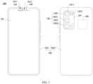
- FIG. 1 is a schematic diagram of a structure of an electronic device 100 according to an embodiment of this application.
- FIG. 1 shows the structure of the electronic device 100 from two perspectives: a front side and a back side of the electronic device 100.
- the electronic device 100 may be an electronic device 100 having a shooting or photographing function, for example, a mobile phone, a tablet computer, a television (or a smart screen), a laptop computer, a video camera, a video recorder, or a camera.
- a mobile phone for example, a mobile phone, a tablet computer, a television (or a smart screen), a laptop computer, a video camera, a video recorder, or a camera.
- a mobile phone for description in this embodiment of this application.
- the electronic device 100 may include a display screen 101 and a housing 102.
- the housing 102 may include a frame 1021 and a rear cover 1022.
- the display screen 101 and the rear cover 1022 are separately located on two sides of the frame 1021.
- the frame 1021 may encircle a periphery of the display screen 101, and the frame 1021 may encircle a periphery of the rear cover 1022.
- the display screen 101, the frame 1021, and the rear cover 1022 may jointly enclose to form a whole machine inner cavity.
- the frame 1021 and the rear cover 1022 may form an integrated structure through assembly, or may be an integrally formed structure.
- the display screen 101 may include a glass cover and a display panel fastened to the glass cover, and the display panel is configured to display an image.
- the electronic device 100 may further include a front-facing camera module 103, an earpiece module 104, a rear-facing camera module 105, a processor 106, and the like that are accommodated in the whole machine inner cavity.
- the processor 106 is electrically connected to the display screen 101, the front-facing camera module 103, the earpiece module 104, and the rear-facing camera module 105.
- the front-facing camera module 103 and the earpiece module 104 may be installed on an upper middle part of the display screen 101.
- the display screen 101 may be provided with a front-facing camera hole 1011 and an earpiece hole 1012.
- the front-facing camera module 103 may capture external light of the electronic device 100 through the front-facing camera hole 1011, to take a selfie.
- the earpiece module 104 may emit sound through the earpiece hole 1012, so that a user can answer a call, make a voice, and the like.
- the rear-facing camera module 105 may be installed on an upper left part of the rear cover 1022.
- the electronic device 100 may further include a camera decorative member 107.
- the camera decorative member 107 is installed on the rear cover 1022, and the camera decorative member 107 is provided with a plurality of light through holes 1071.
- the rear-facing camera module 105 may capture external light through the light through holes 1071 on the camera decorative member 107, to photograph a scene around the electronic device 100.
- installation locations of the front-facing camera module 103 and the rear-facing camera module 105 shown in FIG. 1 are merely examples. The installation locations of the camera modules may not be limited in this application. In some other embodiments, the front-facing camera module 103 and the rear-facing camera module 105 may alternatively be installed at other locations on the electronic device 100.
- the front-facing camera module 103 may be externally installed on an upper left part or an upper right part of the display screen 101.
- the rear-facing camera module 105 may be installed on an upper middle part or an upper right part of the rear cover 1022.
- the front-facing camera module 103 or the rear-facing camera module 105 may be disposed on a movable component in the electronic device 100. By moving the movable component, the movable component may be hidden inside the electronic device 100, or may extend out of the electronic device 100.
- quantities of installed front-facing camera modules 103 and rear-facing camera modules 105 shown in FIG. 1 are merely examples.
- the quantities of installed camera modules may not be limited in this application.
- the electronic device 100 may include more or fewer camera modules.
- FIG. 2 is a schematic diagram of a structure of the electronic device 100 shown in FIG. 1 in an application scenario.
- the rear-facing camera module 105 may include a primary two-dimensional (two-dimensional, 2D) camera 1051 and a secondary 2D camera 1052.
- Both the primary 2D camera 1051 and the secondary 2D camera 1052 may be configured to photograph 2D image information such as a 2D contour, a 2D pattern, and a color (and then grayscale, a shade, and the like) of a target object, to obtain a 2D image of the target object. Jointly using the primary 2D camera 1051 and the secondary 2D camera 1052 helps obtain a high-resolution and high-quality 2D image.
- the rear-facing camera module 105 may further include, for example, a flash light 1053.
- the flash light 1053 may be located near the primary 2D camera 1051 or the secondary 2D camera 1052.
- the flash light 1053 may emit visible light.
- the flash light 1053 may provide light for the primary 2D camera 1051 and/or the secondary 2D camera 1052. For example, in a night or a scenario with dark light, light emitted by the flash light 1053 may be illuminated on the target object, so that light intensity that is captured by the primary 2D camera 1051 and/or the secondary 2D camera 1052 and that is from the target object can be increased.
- the rear-facing camera module 105 may further include a 3D camera 1054.
- the 3D camera 1054 may be configured to photograph a 3D contour of the target object, to obtain a 3D image of the target object.
- the 3D camera 1054 may include a transmitter and a receiver, and the transmitter may be located near the receiver.
- the transmitter may emit infrared light
- the receiver may be a 3D camera lens that can detect (or capture or receive) the infrared light.
- 3D contour information of the target object may be obtained by measuring a direct time of flight (direct time of flight, DTOF) of light from the target object to the receiver.
- the 3D contour information is depth information
- the 3D image is a depth image.
- the transmitter and the receiver are jointly used to measure a direct time of flight of light between the electronic device 100 and the target object.
- light shown by a solid line in the figure
- reflected light shown by a dashed line in the figure.
- a distance between the transmitter and the receiver is a first distance
- a distance between the transmitter and the target object is a second distance
- a distance between the target object and the receiver is a third distance.
- the first distance may be far less than the second distance and the third distance, that is, the first distance may be ignored relative to the second distance and the third distance.
- the direct time of flight of the light from the target object to the receiver may be approximately determined by measuring a direct time of flight of light emitted from the transmitter to the receiver, to obtain the 3D image including the 3D contour information of the target object.
- FIG. 3 is a schematic diagram of synthesizing a 2D image and a 3D image by the electronic device 100 shown in FIG. 1 .
- the electronic device 100 may obtain the 2D image (for example, an image 201 in FIG. 3 ) of the target object through the primary 2D camera 1051 and/or the secondary 2D camera 1052, obtain the 3D image (for example, an image 202 in FIG. 3 ) of the target object through the 3D camera 1054, and obtain, by synthesizing the foregoing 2D image (for example, the image 201 in FIG. 3 ) and the foregoing 3D image (for example, the image 202 in FIG. 3 ), a vivid 3D image (for example, an image 203 in FIG. 3 ) that includes both the 3D contour information and the 2D image information.
- the image 201, the image 202, and the image 203 shown in FIG. 3 are merely examples. Specific parameters (such as a resolution, a pixel size, and a three-dimensional model granularity) of the image may not be limited in this application.
- the structure shown in this embodiment of this application does not constitute a specific limitation on the electronic device 100.
- the electronic device 100 may include more or fewer components than those shown in the figure.
- the electronic device 100 may include more or fewer cameras than those shown in the figure.
- the rear-facing camera module 105 may alternatively include only the 3D camera 1054, where the 3D camera 1054 may further have a capability of photographing the 2D image.
- the electronic device 100 may photograph, through the 3D camera 1054, the vivid 3D image that includes both the 2D image information and the 3D contour information.
- the rear-facing camera module 105 may obtain both the 2D image of the target object and the 3D image of the target object. Therefore, the electronic device 100 may implement applications such as facial recognition, portrait unlocking, gesture recognition, object modeling, a 3D game, and a smart home, thereby helping improve use experience of a user.
- An embodiment of this application provides a TOF apparatus.
- the 3D camera 1054 of the electronic device 100 may use the TOF apparatus.
- a processor 106 of the electronic device 100 is electrically connected to the TOF apparatus, and the processor 106 is configured to form the 3D image of the target object based on an output signal of the TOF apparatus.
- the TOF apparatus includes a transmitter and a receiver, and both the transmitter and the receiver are divided into a plurality of regions.
- the TOF apparatus can capture a plurality of local 3D images corresponding to different regions of the target object (which may also be referred to as a photographed object) in a manner in which the transmitter performs region-based turning-on and the receiver performs region-based detection, and then the electronic device 100 splices the plurality of local 3D images, to obtain the 3D image of the target object.
- the TOF apparatus can implement detection at a longer distance under a peak current allowed by the electronic device 100, and a detection range of the TOF apparatus and the electronic device 100 is larger.
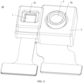
- FIG. 4 is a schematic diagram of a structure of a TOF apparatus 10 in some embodiments according to an embodiment of this application
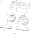
- FIG. 5 is a schematic diagram of a partial exploded structure of the TOF apparatus 10 shown in FIG. 4 .
- the TOF apparatus 10 includes a transmitter 1, a receiver 2, and an outer housing 3.
- the outer housing 3 has a first installation space 31, a second installation space 32, a first through hole 33, and a second through hole 34.
- the first through hole 33 is in communication with the first installation space 31, and the second through hole 34 is in communication with the second installation space 32.
- the transmitter 1 is installed in the first installation space 31 and is fixedly connected to the outer housing 3, and light emitted by the transmitter 1 can be emitted through the first through hole 33.
- the receiver 2 is installed in the second installation space 32 and is fixedly connected to the outer housing 3, and the receiver 2 can receive light through the second through hole 34. Both the transmitter 1 and the receiver 2 are fastened to the outer housing 3, so that the TOF apparatus 10 can form a modular structure, to facilitate installing the TOF apparatus 10 in the electronic device 100.
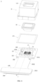
- FIG. 6 is a schematic diagram of a partial exploded structure of the transmitter 1 shown in FIG. 5
- FIG. 7 is a schematic diagram of a cross sectional structure of the transmitter 1 shown in FIG. 5 that is cut along A-A.
- the transmitter 1 includes a housing 11, an optical element 12, a light source 13, a drive chip 14, and a first circuit board assembly 15.
- the housing 11 is fastened on a top side of the first circuit board assembly 15, and the housing 11 and the first circuit board assembly 15 jointly enclose to form an inner cavity 16 of the transmitter.
- the housing 11 is of a hollow structure, a top of the housing 11 has a light outlet hole 111, a bottom of the housing 11 is of an open structure, and the bottom of the housing 11 may be fixedly connected to the first circuit board assembly 15 through a bonding member 171.
- the optical element 12 is located in the inner cavity 16 of the transmitter and is fixedly connected to the housing 11, and the optical element 12 is disposed corresponding to the light outlet hole 111.
- the optical element 12 may cover the light outlet hole 111, and a bonding member (not shown in the figure) may be disposed between the top of the optical element 12 and an inner wall of the housing 11.
- Both the drive chip 14 and the light source 13 are located in the inner cavity 16 of the transmitter, the drive chip 14 may be fastened to the first circuit board assembly 15, and the light source 13 may be fastened on a top side of the drive chip 14.
- the optical element 12 is located on a light emitting path of the light source 13. In this embodiment, after light emitted by the light source 13 passes through the optical element 12, the light is emitted from the transmitter 1 through the light outlet hole 111.
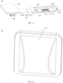
- FIG. 8 is a schematic diagram of a structure of the light source 13 shown in FIG. 6 .
- the light source 13 includes a plurality of light emitting units 131, and each light emitting unit 131 may emit light, for example, may emit invisible light such as infrared light.
- the plurality of light emitting units 131 may work independently, and the plurality of light emitting units 131 may be turned on in turn according to a specific time sequence, to emit light in turn. For example, there may be 4 to 20 light emitting units 131.
- the plurality of light emitting units 131 of the light source 13 may be arranged in an N ⁇ 1 manner, where N is an integer greater than or equal to 2.
- the plurality of light emitting units 131 are arranged in a first direction X, each light emitting unit 131 extends in a second direction Y, and the second direction Y is perpendicular to the first direction X.
- a thickness direction of the light source 13 is a third direction Z, and the third direction Z is perpendicular to the first direction X and the second direction Y.
- Each light emitting unit 131 is approximately in a strip shape.
- the light source 13 may be, but is not limited to, a vertical-cavity surface-emitting laser (vertical-cavity surface-emitting laser, VCSEL).
- the light source 13 includes an anode pad 132 and a cathode pad 133, the anode pad 132 is located on a light emitting side of the light source 13, and the cathode pad 133 is located on a non-light emitting side of the light source 13.
- there are a plurality of anode pads 132 each light emitting unit 131 includes two anode pads 132, and the two anode pads 132 are respectively located at two ends of the light emitting unit 131.
- Each light emitting unit 131 includes a light emitting region 134, and two anode pads 132 are respectively located on two sides of the light emitting region 134.
- there is one cathode pad 133 and the plurality of light emitting units 131 share the one cathode pad 133.
- a distance between light emitting regions 134 of two adjacent light emitting units 131 may be within a range of about 30 micrometers ( ⁇ m) to 50 micrometers, for example, may be 40 micrometers.
- FIG. 9 is a schematic diagram of an assembly structure of the light source 13 and the drive chip 14 shown in FIG. 6
- FIG. 10 is a schematic diagram of the structure shown in FIG. 9 that is cut along B-B.
- the light source 13 and the drive chip 14 are disposed in a stacked manner, and the non-light emitting side of the light source 13 is fastened to the drive chip 14.
- the drive chip 14 is configured to turn on the plurality of light emitting units 131 in turn according to a specific time sequence.
- the drive chip 14 includes a first pad 141 and a second pad 142.
- the first pad 141 is located on a side of the drive chip 14 close to the light source 13, and is located around the light source 13.
- the first pad 141 is connected to the anode pad 132 through a conductive wire 18.
- the conductive wire 18 may be a gold wire.
- the second pad 142 is located on the side of the drive chip 14 close to the light source 13 and is disposed facing the non-light emitting side of the light source 13, and the second pad 142 is connected to the cathode pad 133 through a conductive adhesive 19.
- the conductive adhesive 19 may implement an electrical connection function, or may implement a bonding and fastening function.
- the conductive adhesive 19 may be a conductive silver adhesive.
- the light source 13 can be electrically connected to the drive chip 14 through the connection between the anode pad 132 and the first pad 141 and the connection between the cathode pad 133 and the second pad 142, so that the drive chip 14 can turn on the light source 13 to control the light source 13 to emit light.
- the light source 13 and the drive chip 14 are disposed in a stacked manner, and are arranged in a compact manner, which facilitates a miniaturization design of the transmitter 1 and the TOF apparatus 10.
- the light source 13 and the drive chip 14 are disposed in the stacked manner, so that a wiring distance between the light source 13 and the drive chip 14 may also be greatly reduced (for example, a length of the conductive wire 18 is obviously shortened), thereby effectively improving a light waveform of the light source 13 and ensuring performance of the transmitter 1.
- the transmitter 1 uses a nanosecond (ns)-level pulse width to drive light emission.
- a pulse width of a light waveform, a rising waveform of a light waveform, and a falling waveform of a light waveform of light emitted by the transmitter 1 have obvious impact on ranging precision of the TOF apparatus 10, and a factor that affects the light waveform is a wiring inductor between the drive chip 14 and the light source 13. If there is a long loop between the light source 13 and the drive chip 14, a high wiring inductor is introduced. As a result, a rising speed of the light waveform slows down, a rising time increases, and the ranging precision of the TOF apparatus 10 decreases.
- a wiring distance between the light source 13 and the drive chip 14 is very short, a light waveform of the light source 13 can be effectively improved, and the ranging precision of the TOF apparatus 10 can be improved.
- first pads 141 there are a plurality of first pads 141, the plurality of first pads 141 are in groups of two, each group of first pads 141 correspond to one light emitting unit 131, and two first pads 141 in a same group are respectively located on two sides of a corresponding light emitting unit 131 and are respectively connected to two anode pads 132 of the corresponding light emitting unit 131.
- the anode pad 132 of the light emitting unit 131 of the light source 13 is connected to the first pad 141 of the drive chip 14 by binding conductive wires 18 on both sides, so that the drive chip 14 can simultaneously turn on or nearly simultaneously turn on an entire light emitting region 134 of the light emitting unit 131, to reduce a detection error caused by uneven turning-on time of the plurality of light emitting units 131 of the transmitter 1, and improve the ranging precision and photographing quality of the TOF apparatus 10.
- conduction may be implemented between the corresponding anode pad 132 and the first pad 141 through two conductive wires 18, to improve reliability of the connection between the anode pad 132 and the first pad 141.
- each light emitting unit 131 may alternatively include one anode pad 132.
- the anode pad 132 is connected to one first pad 141 of the drive chip 14 through the conductive wire 18, to implement an electrical connection between the drive chip 14 and the light source 13.
- Each light emitting unit 131 includes at least one cathode pad 133.
- the cathode pad 133 is connected to the second pad 142 of the drive chip 14, to implement the electrical connection between the drive chip 14 and the light source 13.
- the drive chip 14 may be configured to supply power to the light source 13, to drive light emission by using a nanosecond-level pulse width.
- the drive chip 14 may be further configured to implement functions such as laser safety monitoring and power supply voltage monitoring.
- the drive chip 14 may be further configured to implement optical power control, pulse width adjustment, and the like for the light source 13.
- a function of the drive chip 14 is not strictly limited in this embodiment of this application.
- FIG. 11 is a schematic diagram of a cross section of the first circuit board assembly 15, the drive chip 14, and the light source 13 shown in FIG. 6 that are cut along C-C.
- the first circuit board assembly 15 includes a first circuit board 151, a first reinforcement plate 152, a second reinforcement plate 153, a first electrical connector 154, and a plurality of first components 155.
- the first circuit board 151 may be a flexible-rigid circuit board.
- the first circuit board 151 may include a first rigid board part 1511, a first flexible board part 1512, and a second rigid board part 1513 that are sequentially connected. Rigidity of the first rigid board part 1511 and rigidity of the second rigid board part 1513 are greater than rigidity of the first flexible board part 1512.
- the first rigid board part 1511 of the first circuit board 151 has a through hole 1514, and the through hole 1514 penetrates the first rigid board part 1511 in a thickness direction of the first rigid board part 1511.
- the first reinforcement plate 152 is fastened on a side of the first rigid board part 1511 of the first circuit board 151 and covers the through hole 1514.
- the first reinforcement plate 152 may be fixedly connected to the first rigid board part 1511 through a bonding member 173.
- the drive chip 14 is at least partially located in the through hole 1514, and a side of the drive chip 14 away from the light source 13 is fastened on the first reinforcement plate 152.
- the drive chip 14 may be entirely located in the through hole 1514, and the light source 13 may be entirely or partially located in the through hole 1514.
- the drive chip 14 may be fixedly connected to the first reinforcement plate 152 through a bonding member 174.
- an arrangement manner of the drive chip 14, the light source 13, and the first circuit board 151 assembly 15 helps reduce a thickness of the transmitter 1 and implement miniaturization of the TOF apparatus 10.
- the plurality of first components 155 are fastened on a side of the first rigid board part 1511 opposite to the first reinforcement plate 152, and the plurality of first components 155 may be arranged around the through hole 1514.
- the plurality of first components 155 may include a matching component of the drive chip 14.
- the plurality of first components 155 may include one or more of a capacitor, an inductor, and a resistor.
- the first electrical connector 154 is fastened on a side of the second rigid board part 1513, and the first electrical connector 154 is configured to be electrically connected to an external component of the TOF apparatus 10.
- the first electrical connector 154 may be an electrical connector of a type such as a board-to-board connector. This is not strictly limited in this embodiment of this application.
- the second reinforcement plate 153 is fastened on another side of the second rigid board part 1513, and is configured to increase structural strength of the first circuit board 151 assembly 15.
- the first reinforcement plate 152 and/or the second reinforcement plate 153 may be a metal plate such as a steel plate, or may be a plastic plate with high rigidity.
- the first rigid board part 1511 may not be provided with the through hole 1514, and the drive chip 14 is fastened on a top side of the first rigid board part 1511. In this case, if the structural strength of the first rigid board part 1511 is sufficient, the first reinforcement plate 152 may not be disposed on the first circuit board 151 assembly 15. In some other embodiments, if the structural strength of the second rigid board part 1513 is sufficient, the second reinforcement plate 153 may either not be disposed on the first circuit board 151 assembly 15.
- the first circuit board 151 may alternatively be a flexible circuit board.
- the flexible circuit board includes a first part, a second part, and a third part that are sequentially connected.
- first part and a location relationship between the first part and another structure refer to the first rigid board part 1511 in the foregoing embodiment.
- second rigid board part 1513 in the foregoing embodiment For a connection relationship and a location relationship between the third part and another structure, refer to the second rigid board part 1513 in the foregoing embodiment. Details are not described herein again.
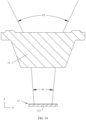
- FIG. 12 is a schematic diagram of a structure of the optical element 12 shown in FIG. 6 from another angle.
- the optical element 12 may include a light inlet surface 121 and a light outlet surface 122, and the light outlet surface 122 is disposed opposite to the light inlet surface 121.
- the light inlet surface 121 may be a curved surface, and a middle part of the light inlet surface 121 protrudes in a direction away from the light outlet surface 122.
- An optical signal emitted by the light source 13 enters the optical element 12 through the light inlet surface 121, and is emitted from the optical element 12 through the light outlet surface 122.
- the transmitter 1 implements emitting the optical signal.
- the optical element 12 is configured to change a propagation direction of the optical signal.
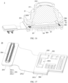
- FIG. 13 is a schematic diagram of the light source 13 and the optical element 12 in FIG. 7
- FIG. 14 is a schematic diagram of the light source 13 and the optical element 12 shown in FIG. 13 from another angle.
- a cross section shown in FIG. 13 is parallel to the first direction X
- a cross section shown in FIG. 14 is parallel to the second direction Y.
- the optical element 12 is located on light emitting paths of the plurality of light emitting units 131 of the light source 13, and the optical element 12 is configured to enable light emitted by the plurality of light emitting units 131 to form a plurality of projection fields of view in a one-to-one correspondence.
- the plurality of projection fields of view are arranged in the first direction X.
- the plurality of projection fields of view jointly form a total projection field of view of the transmitter 1.
- FIG. 13 simply shows, in the first direction X, a projection field of view formed after an emission field of view of a single light emitting unit 131 passes through the optical element 12, and the total projection field of view of the transmitter 1 formed after an emission field of view of the light source 13 passes through the optical element 12.
- the 14 simply shows, in the second direction Y, a projection field of view formed after the emission field of view of the single light emitting unit 131 passes through the optical element 12, where the emission field of view of the light source 13 is the same as the emission field of view of the single light emitting unit 131, and the total projection field of view of the transmitter 1 is the same as the projection field of view of the single light emitting unit 131.
- the angle of view of the single light emitting unit 131 shrinks in the first direction X and expands in the second direction Y. That is, in the first direction X, an angle of view a2 of the projection field of view of the light emitting unit 131 is less than an angle of view a1 of the emission field of view of the light emitting unit 131; and in the second direction Y, an angle of view b2 of the projection field of view of the light emitting unit 131 is greater than an angle of view b1 of the emission field of view of the light emitting unit 131.
- the angle of view a1 of the emission field of view of the light emitting unit 131 may be approximately within a range of 20° to 25°, and the angle of view a2 of the projection field of view of the light emitting unit 131 may be approximately within a range of 4° to 5°.
- the angle of view b1 of the emission field of view of the light emitting unit 131 may be approximately within a range of 20° to 25°, and the angle of view b2 of the projection field of view of the light emitting unit 131 may be approximately within a range of 50° to 60°.
- the angle of view of the light source 13 expands in both the first direction X and the second direction Y.
- an angle of view (a4, b2) of the total projection field of view of the transmitter 1 is greater than the angle of view of the emission field of view of the light source 13.
- An angle of view of the light source 13 in the first direction X and the second direction Y is equal to an angle of view (a3, b1) of the single light emitting unit 131.
- angles of view a4 of the plurality of projection fields of view (that is, the total projection field of view of the transmitter 1) in the first direction X may be within a range of 65° to 70°
- angles of view b2 of the plurality of projection fields of view in the second direction Y may be within a range of 50° to 60°.
- the angle of view of the total projection field of view of the transmitter 1 may be 78°.
- a structure of the optical element 12 may be implemented in a plurality of manners.
- the optical element 12 may be formed by assembling a plurality of transparent structures, or may be an integrally formed structure.
- a specific implementation structure of the optical element 12 is not strictly limited.
- the optical element 12 can enable the plurality of projection fields of view to satisfy the following conditions as much as possible: for example, having a same spatial location, better uniformity, and better window efficiency.
- energy of a beam emitted by the transmitter 1 can be distributed in a valid region (that is, an expected total projection field of view of the transmitter 1) as much as possible, so that the window efficiency can be greater than or greater than 60%, to improve energy utilization.
- FIG. 15 is a schematic diagram of a partial exploded structure of the receiver 2 shown in FIG. 5
- FIG. 16 is a schematic diagram of a cross sectional structure of the receiver 2 shown in FIG. 5 that is cut along D-D.
- the receiver 2 includes a camera lens 21, a base 22, a light filter 23, an image sensor 24, and a second circuit board assembly 25.
- the camera lens 21 may be fastened on a side of the base 22 through a bonding member 261.
- the camera lens 21 may be a fixed-focal-length camera lens (which may also be referred to as a fixed-focus camera lens) or a zoom camera lens.
- FIG. 15 and FIG. 16 are schematic diagrams using an example in which the camera lens 21 is a fixed-focal-length camera lens.
- the camera lens 21 may alternatively be a short-focus camera lens, a medium long-focus camera lens, a long-focus camera lens, or the like.
- the camera lens 21 may include a lens tube 211 and one or more lenses (lens) 212 disposed in the lens tube 211.
- the lens tube 211 is of a hollow structure and has openings at two ends. The openings at the two ends are respectively a light inlet and a light outlet. The light outlet is disposed close to the base 22.
- An optical signal outside the receiver 2 can be emitted into the camera lens 21 from the light inlet. After passing through the one or more lenses 212, the optical signal is emitted out of the camera lens 21 from the light outlet.
- the base 22 is located on a light emitting side of the camera lens 21.
- the one or more lenses 212 can change a propagation direction of light, so that the camera lens 21 can converge the light and emit the light to a predetermined region.
- the one or more lenses 212 may include a plastic (plastic) lens and/or a glass (glass) lens.
- the one or more lenses 212 may include a spherical lens and/or an aspheric lens.
- the lens tube 211 shown in FIG. 15 and FIG. 16 is merely an example. A structure, a size, and the like of the lens tube 211 may not be limited in this embodiment of this application.
- the lens 212 shown in FIG. 16 is merely an example. A quantity of lenses 212, a structure of the lens 212, and the like may not be limited in this embodiment of this application.
- the camera lens 21 may alternatively be a zoom camera lens.
- the camera lens 21 may further include a motor, and the motor is configured to drive the camera lens 21 to move in an optical axis direction, to implement automatic focusing.
- the second circuit board assembly 25 may be fastened on another side of the base 22 through a bonding member 262.
- the base 22 and the second circuit board assembly 25 jointly enclose to form an accommodating space.
- a through hole 221 is disposed in a middle part of the base 22, and the through hole 221 is in communication with the accommodating space.
- the image sensor 24 is located on the light emitting side of the camera lens 21.
- the image sensor 24 may be located in the accommodating space and fastened to the second circuit board assembly 25.
- the image sensor 24 may be bonded to the second circuit board assembly 25 through a bonding layer 263, or the image sensor 24 may be fastened to the second circuit board assembly 25 by welding.
- a light sensing side of the image sensor 24 is disposed facing the camera lens 21.
- the image sensor 24 may be a semiconductor chip. Hundreds of thousands to millions of photodiodes are disposed on a light sensing surface of the image sensor 24, and the photodiode may be, for example, a single photon avalanche diode (single photon avalanche diode, SPAD). The photodiode generates charges when exposed to light, thereby converting an optical signal into an electrical signal.
- the image sensor 24 may be a charge coupled device (charge coupled device, CCD), a complementary metal-oxide semiconductor (complementary metal-oxide semiconductor, CMOS), or the like.
- the light filter 23 is located on the light emitting side of the camera lens 21 and is fastened to the base 22, where the light filter 23 may be accommodated in the accommodating space.
- the light filter 23 may alternatively be located on a side of the base 22 facing the camera lens 21, where the light filter 23 may cover the through hole 221 of the base 22.
- a peripheral edge of the light filter 23 may be fixedly connected to the base 22 through a bonding member 264.
- the light filter 23 may eliminate unnecessary light (for example, visible light) projected onto the image sensor 24, and prevent the image sensor 24 from generating an image defect such as a ripple, to improve an effective resolution and image reproduction of the image sensor 24.
- a working principle of the receiver 2 may be as follows: Reflected light formed by reflection by a target object may pass through the one or more lenses 212 in the lens tube 211, then pass through the light filter 23, and be projected to the light sensing surface of the image sensor 24.
- the image sensor 24 may convert the optical signal into the electrical signal, to obtain 3D contour information of the target object, and then transmit the 3D contour information to a component such as the processor 106 of the electronic device 100 by using the second circuit board assembly 25, to perform subsequent image processing.
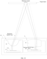
- FIG. 17 is a schematic diagram of a structure of the second circuit board assembly 25 shown in FIG. 15 from another angle.
- the second circuit board assembly 25 includes a second circuit board 251, a third reinforcement plate 252, a fourth reinforcement plate 253, a second electrical connector 254, and a plurality of second components 255.
- a non-light sensing side of the image sensor 24 may be fastened on the second circuit board 251.
- the third reinforcement plate 252 is fastened on a side of the second circuit board 251 away from the image sensor 24, and the third reinforcement plate 252 is provided with one or more vias 2521.
- the plurality of second components 255 are located in the one or more vias 2521 and are fastened on the second circuit board 251.
- the second circuit board assembly 25 uses a component back-mounted design, which helps reduce space occupied by the second circuit board assembly 25 in a direction parallel to a board surface, so that the receiver 2 and the TOF apparatus 10 are more easily miniaturized.
- the third reinforcement plate 252 may further protect the plurality of second components 255, prevent collision, and increase structural strength of the circuit board.
- Projections of the plurality of second components 255 on the second circuit board 251 may at least partially overlap a projection of the image sensor 24 on the second circuit board 251, to further improve space utilization of the second circuit board assembly 25, and facilitate miniaturization of the receiver 2 and the TOF apparatus 10. It may be understood that at least partial overlapping may include two cases: entire overlapping and partial overlapping. The entire overlapping means that a projection of one entirely covers a projection of the other.
- the second circuit board 251 may be a flexible-rigid circuit board.
- the second circuit board 251 may include a third rigid board part 2511, a second flexible board part 2512, and a fourth rigid board part 2513 that are sequentially connected. Rigidity of the third rigid board part 2511 and rigidity of the fourth rigid board part 2513 are greater than rigidity of the second flexible board part 2512.
- the non-light sensing side of the image sensor 24 may be fastened on a side of the third rigid board part 2511, the third reinforcement plate 252 may be fastened on another side of the third rigid board part 2511 through a bonding member 266, and the plurality of second components 255 may be fastened on the third rigid board part 2511 in a manner such as welding.
- the plurality of second components 255 may include a matching component of the image sensor 24.
- the plurality of second components 255 may include one or more of a capacitor, an inductor, and a resistor.
- the second electrical connector 254 is fastened on a side of the fourth rigid board part 2513, and the second electrical connector 254 is configured to be electrically connected to an external component of the TOF apparatus 10.
- the second electrical connector 254 may be an electrical connector of a type such as a board-to-board connector. This is not strictly limited in this embodiment of this application.
- the fourth reinforcement plate 253 is fastened on another side of the fourth rigid board part 2513, and is configured to increase structural strength of the second circuit board assembly 25.
- the third reinforcement plate 252 and/or the fourth reinforcement plate 253 may be a metal plate such as a steel plate, or may be a plastic plate with high rigidity.
- the second circuit board 251 may alternatively be a flexible circuit board.
- the flexible circuit board includes a first part, a second part, and a third part that are sequentially connected.
- the third rigid board part 2511 in the foregoing embodiment.
- the fourth rigid board part 2513 in the foregoing embodiment. Details are not described herein again.
- FIG. 18 is a schematic block diagram of the image sensor 24 shown in FIG. 15 .
- FIG. 18 merely schematically shows a plurality of functional regions (or referred to as functional modules) of the image sensor 24, and does not limit an actual structure, an actual circuit, and the like of the image sensor 24.
- the image sensor 24 may include a light sensing circuit 241, a logic control circuit 242, a data storage and conversion circuit 243, and a power supply circuit 244.
- the light sensing circuit 241 includes a plurality of light sensing units 2411, and the plurality of light sensing units 2411 may work independently.
- a quantity of the light sensing units 2411 is the same as a quantity of the light emitting units 131 of the light source 13.
- Each light sensing unit 2411 may include a plurality of single-photon detectors (not shown in the figure).
- the logic control circuit 242 is configured to start the plurality of light sensing units 2411 in turn according to a specific time sequence.
- a started light sensing unit 2411 can convert an optical signal into an electrical signal.
- the logic control circuit 242 may configure the power supply circuit 244, so that the power supply circuit 244 supplies power to the light sensing units 2411 in turn according to the specific time sequence.
- the image sensor 24 uses a region-based startup design. Compared with a conventional solution in which the image sensor is started as a whole, in this embodiment, a single-photon detector of another light sensing unit 2411 in a non-started state of the image sensor 24 can avoid a waste of power consumption caused by incorrect triggering due to ambient light, thereby reducing energy consumption of the receiver 2. In addition, the image sensor 24 uses the region-based startup design, which also helps avoid problems such as dark count and crosstalk.
- the data storage and conversion circuit 243 is configured to calculate and buffer depth data.
- the data storage and conversion circuit 243 includes a time-to-digital converter (time-to-digital converter, TDC) and a memory.
- the time-to-digital converter is electrically connected to the plurality of light sensing units 2411, and is configured to convert analog signals output by the plurality of light sensing units 2411 into digital signals represented by time.
- the memory is electrically connected to the time-to-digital converter, and is configured to store the digital signals.
- the time-to-digital converter is configured to determine a time at which the light sensing unit 2411 receives the optical signal, and then accordingly calculate a time difference between a time at which the TOF apparatus 10 emits the optical signal and a time at which the TOF apparatus 10 receives the optical signal.
- the logic control circuit 242 and the power supply circuit 244 may be located around the light sensing circuit 241, and the data storage and conversion circuit 243 may be located on a non-light sensing side of the light sensing circuit 241, that is, located below the light sensing circuit 241, and is stacked with the light sensing circuit 241.
- a single light sensing unit 2411 may include P ⁇ Q single-photon detectors, and the time-to-digital converter may include P ⁇ Q units, where both P and Q are positive integers.
- a quantity of units of the time-to-digital converter corresponds to a quantity of single-photon detectors of the light sensing unit 2411, so that an area of the image sensor 24 can be reduced when a requirement for calculating and buffering the depth data is satisfied, thereby facilitating miniaturization of the receiver 2 and the TOF apparatus 10.
- the image sensor 24 uses a video graphics array (video graphics array, VGA) with a resolution of 640 ⁇ 480. Assuming that the light source 13 includes 10 light emitting units 131, the image sensor 24 correspondingly includes 10 light sensing units 2411. Each light sensing unit 2411 has a resolution of 640 ⁇ 48. In this case, the quantity of units of the time-to-digital converter may be 640 ⁇ 48.
- VGA video graphics array
- FIG. 19 is a schematic diagram of an application of the TOF apparatus 10 shown in FIG. 4
- FIG. 20 is another schematic diagram of the application the TOF apparatus 10 shown in FIG. 4
- FIG. 19 briefly shows a structure and an application scenario of the TOF apparatus 10
- FIG. 20 briefly shows a basic composition and an application scenario of the TOF apparatus 10. It may be understood that optical paths shown in FIG. 19 and FIG. 20 are brief schematic diagrams, and do not constitute a limitation on an actual optical path. In actual use, the TOF apparatus 10 may have another optical path. This is not strictly limited in this application.
- the light source 13 of the transmitter 1 includes a plurality of light emitting units 131, and a drive chip (not shown in the figure) is configured to turn on the plurality of light emitting units 131 in turn according to a specific time sequence.
- An optical element 12 is located on light emitting paths of the plurality of light emitting units 131, and the optical element 12 is configured to enable light emitted by the plurality of light emitting units 131 to form a plurality of projection fields of view in a one-to-one correspondence.
- the plurality of projection fields of view are for covering a target object.
- the target object is located in a detection range of the TOF apparatus 10, and the detection range of the TOF apparatus 10 is greater than 10 centimeters.
- a camera lens 21 of the receiver 2 is configured to receive light reflected by the target object and form a plurality of sensing fields of view.
- the plurality of sensing fields of view are in a one-to-one correspondence with the plurality of projection fields of view.
- An image sensor 24 is located on a light emitting side of the camera lens 21.
- the image sensor 24 includes a plurality of light sensing units 2411 and a logic control circuit (not shown in the figure), the plurality of sensing fields of view cover the plurality of light sensing units 2411 in a one-to-one correspondence, the logic control circuit is configured to start the plurality of light sensing units 2411 in turn according to a specific time sequence, and a start time sequence of each light sensing unit 2411 is the same as a turn-on time sequence of a corresponding light emitting unit 131.
- the plurality of light emitting units 131 of the light source 13 include a first light emitting unit, a second light emitting unit, ..., and a K th light emitting unit, where K is a positive integer greater than 2.
- Light emitted by the plurality of light emitting units 131 forms a plurality of projection fields of view after passing through the optical element 12.
- the plurality of projection fields of view include a first projection field of view, a second projection field of view, ..., and a K th projection field of view that are in a one-to-one correspondence with the plurality of light emitting units 131.
- the plurality of projection fields of view cover a plurality of detection regions of the target object, the plurality of detection regions include a first detection region, a second detection region, ..., and a K th detection region that are in a one-to-one correspondence with the plurality of projection fields of view, and the plurality of detection regions jointly form the target object.
- light emitted by the transmitter 1 is received by the camera lens 21.
- a plurality of sensing fields of view are formed, where the plurality of sensing fields of view include a first sensing field of view, a second sensing field of view, ..., and a K th sensing field of view that are in a one-to-one correspondence with the plurality of detection regions.
- the plurality of light sensing units 2411 include a first light sensing unit, a second light sensing unit, ..., and a K th light sensing unit that are in a one-to-one correspondence with the plurality of sensing fields of view, and the plurality of sensing fields of view cover the plurality of light sensing units 2411 in a one-to-one correspondence.
- the plurality of light emitting units 131, the plurality of projection fields of view, the plurality of detection regions of the target object, the plurality of sensing fields of view, and the plurality of light sensing units 2411 are disposed in groups in a one-to-one correspondence.
- the drive chip turns on the plurality of light emitting units 131 according to a specific time sequence
- the logic control circuit starts the plurality of light sensing units 2411 according to a specific time sequence
- a start time sequence of each light sensing unit 2411 is the same as a turn-on time sequence of a corresponding light emitting unit 131.
- the logic control circuit starts the first light sensing unit; when the drive chip turns on the second light emitting unit, the logic control circuit starts the second light sensing unit; ...; and when the drive chip turns on the K th light emitting unit, the logic control circuit starts the K th light sensing unit.
- the TOF apparatus 10 obtains the 3D contour information of the plurality of detection regions of the target object in a manner in which the transmitter 1 performs region-based turning-on and the receiver 2 performs region-based detection.
- the TOF apparatus 10 is electrically connected to a processor of the electronic device 100.
- the processor can form a local 3D image of the target object based on the 3D contour information of each detection region, and then splices a plurality of local 3D images, to obtain a 3D image of the target object.
- the processor 106 can form the 3D image of the target object based on an output signal of the TOF apparatus 10.
- the target object has a plurality of detection regions
- the TOF apparatus 10 separately obtains 3D contour information of the plurality of detection regions through a plurality of times of detection.
- a light emitting unit 131 of the transmitter 1 repeatedly flashes for thousands of times at a fixed frequency, and a corresponding light sensing unit 2411 of the image sensor 24 of the receiver 2 is continuously in a started state, to complete exposure of a corresponding detection region.
- the receiver 2 sends a plurality of time-of-flight distribution histograms to the processor of the electronic device 100. Then, next detection is started until exposure of the plurality of detection regions of the target object is completed.
- the processor forms the local 3D image of the detection region according to the time-of-flight distribution histogram formed during each exposure, and then splices the plurality of local 3D images to form the 3D image of the target object, to complete detection and capturing of a frame of image.
- two adjacent projection fields of view form two adjacent detection regions on the target object, and the two detection regions are partially staggered and partially overlapped.
- an overlapped part of the two adjacent detection regions form redundancy, so that a risk of insufficient detection precision caused by a factor such as an assembly error of the TOF apparatus 10 can be reduced, and a black edge region is avoided at an intersection location of the two adjacent detection regions, so that the TOF apparatus 10 has high detection precision and better imaging quality.
- a proportion of a staggered part of two adjacent detection regions is greater than a proportion of the overlapped part of the two detection regions.
- the proportion of the overlapped part of the two adjacent detection regions may be approximately within a range of 5% to 20%.
- FIG. 21 is a schematic diagram of a working procedure of forming a 3D image by an electronic device according to an embodiment of this application.
- the electronic device includes the TOF apparatus shown in the foregoing embodiments.
- a process in which the TOF apparatus of the electronic device detects one detection region of the target object may include 1k to 10k flash detection processes.
- One flash detection process may include: The light emitting unit emits a first pulse; the light sensing unit is in the started state and the light sensing unit converts an optical signal sensed by the light sensing unit into an electrical signal and outputs the electrical signal; and a data storage and conversion circuit receives the electrical signal, and the data storage and conversion circuit processes and stores data.
- the data storage and conversion circuit sends the time-of-flight histogram to the processor of the electronic device, so that the detection process is performed.
- a pulse width of a pulse of the light emitting unit may be within a range from 1 nanosecond to 5 nanoseconds.
- a plurality of time-of-flight histograms are output in each detection process, and the plurality of time-of-flight histograms are in a one-to-one correspondence with a plurality of single-photon detectors in one light sensing unit.
- the processor can form, based on the plurality of time-of-flight histograms, a local 3D image of the target object corresponding to the light sensing unit.
- the TOF apparatus may sequentially detect the plurality of detection regions according to a specific time sequence. In each detection process, a corresponding time-of-flight histogram is output to the processor.
- the processor forms the local 3D image of the target object based on the time-of-flight histogram, and then splices the plurality of local 3D images to form the 3D image of the target object.
- a specific process refer to FIG. 21 . Details are not described herein again.
- the TOF apparatus uses a manner of region-based turning-on and region-based detection, and detects local regions of the target object for a plurality of times, to detect all regions of the target object. Therefore, a peak current can be effectively shared in the plurality of times of detection of the TOF apparatus, and each detection process of the TOF apparatus can be implemented by using only a low peak current. Therefore, when the electronic device can provide a specific peak current, the TOF apparatus in this embodiment can implement detection at a longer distance, and the TOF apparatus and the electronic device have a wider detection range and can also be better applicable to indoor environment and outdoor environment detection. In addition, an effective power per unit area of the TOF apparatus is also high, which helps improve a resolution of the TOF apparatus, so that the TOF apparatus implements high-resolution detection.
- the TOF apparatus in this embodiment of this application may use a design solution of delaying startup at a receiver, so that startup at the image sensor is later than startup at a light source, and a time period in which a crosstalk problem may occur is skipped, to reduce a risk of crosstalk occurrence and improve detection precision.
- the following provides an example for description.
- FIG. 22 is a schematic block diagram of a partial structure of the TOF apparatus 10 shown in FIG. 4 .
- a logic control circuit 242 of an image sensor 24 of the receiver 2 is electrically connected to a drive chip 14 of the transmitter 1.
- the logic control circuit 242 includes an instruction module 2421 and a drive module 2422.
- the drive module 2422 is electrically connected to the instruction module 2421.
- the instruction module 2421 is configured to send a turn-on instruction to the drive chip 14, where the turn-on instruction indicates the drive chip 14 to turn on a preset light emitting unit 131.
- the drive module 2422 is configured to start the light sensing unit 2411.
- the drive module 2422 is configured to start a preset light sensing unit 2411 with a delay of 0.1 ns to 1 ns, where the preset light sensing unit 2411 corresponds to the preset light emitting unit 131.
- the logic control circuit 242 of the image sensor 24 controls the light sensing unit 2411 to start with a delay of 0.1 ns to 1 ns, the light sensing unit 2411 skips a time period in which a crosstalk problem may occur. Therefore, a problem that the image sensor 24 is incorrectly triggered due to short-distance clutter light can be avoided, and a risk of crosstalk occurrence is reduced, to improve the detection precision of the TOF apparatus 10.
- the logic control circuit 242 may send the turn-on instruction to the drive chip 14 through low-voltage differential signaling (low-voltage differential signaling, LVDS).
- low-voltage differential signaling low-voltage differential signaling, LVDS
- the plurality of light emitting units are arranged in an Nx1 manner, and the plurality of detection fields of view of the transmitter, the plurality of detection regions of the target object, the plurality of sensing fields of view of the receiver, and the plurality of light sensing units of the image sensor may be correspondingly arranged in the Nx1 manner.
- the plurality of light emitting units may alternatively be arranged in an N ⁇ M manner, where M and N are integers greater than or equal to 2.
- the plurality of detection fields of view of the transmitter, the plurality of detection regions of the target object, the plurality of sensing fields of view of the receiver, and the plurality of light sensing units of the image sensor may be correspondingly presented in the N ⁇ M arrangement manner.
- the TOF apparatus is implemented by using a direct time of flight technology.
- the TOF apparatus in this embodiment may alternatively be implemented by using an indirect time of flight (indirect time of flight, ITOF) technology.
- ITOF indirect time of flight
- a working principle of the indirect time of flight technology is: A phase offset between a waveform of an optical signal emitted by a transmitter and a waveform of an optical signal received by a receiver is calculated, and then a distance between a target object and a TOF apparatus is calculated based on the phase offset.
Landscapes
- Engineering & Computer Science (AREA)
- Physics & Mathematics (AREA)
- Computer Networks & Wireless Communication (AREA)
- General Physics & Mathematics (AREA)
- Radar, Positioning & Navigation (AREA)
- Remote Sensing (AREA)
- Multimedia (AREA)
- Signal Processing (AREA)
- Electromagnetism (AREA)
- Optical Radar Systems And Details Thereof (AREA)
- Studio Devices (AREA)
Applications Claiming Priority (2)
| Application Number | Priority Date | Filing Date | Title |
|---|---|---|---|
| CN202011431118.1A CN114615397B (zh) | 2020-12-09 | 2020-12-09 | Tof装置及电子设备 |
| PCT/CN2021/135992 WO2022121879A1 (fr) | 2020-12-09 | 2021-12-07 | Appareil à tof et dispositif électronique |
Publications (2)
| Publication Number | Publication Date |
|---|---|
| EP4246952A1 true EP4246952A1 (fr) | 2023-09-20 |
| EP4246952A4 EP4246952A4 (fr) | 2024-04-17 |
Family
ID=81855916
Family Applications (1)
| Application Number | Title | Priority Date | Filing Date |
|---|---|---|---|
| EP21902584.8A Pending EP4246952A4 (fr) | 2020-12-09 | 2021-12-07 | Appareil à tof et dispositif électronique |
Country Status (4)
| Country | Link |
|---|---|
| US (1) | US12372657B2 (fr) |
| EP (1) | EP4246952A4 (fr) |
| CN (1) | CN114615397B (fr) |
| WO (1) | WO2022121879A1 (fr) |
Families Citing this family (2)
| Publication number | Priority date | Publication date | Assignee | Title |
|---|---|---|---|---|
| CN115184956B (zh) * | 2022-09-09 | 2023-01-13 | 荣耀终端有限公司 | Tof传感器系统和电子设备 |
| CN117197261B (zh) * | 2023-11-07 | 2024-02-27 | 深圳市千岩科技有限公司 | 氛围灯设备及其取色方法和相应的装置、介质 |
Family Cites Families (27)
| Publication number | Priority date | Publication date | Assignee | Title |
|---|---|---|---|---|
| JP4378004B2 (ja) | 1999-12-02 | 2009-12-02 | キヤノン株式会社 | 色分解光学系及びそれを用いたテレビカメラ |
| CN102131051B (zh) | 2010-12-28 | 2012-11-28 | 惠州Tcl移动通信有限公司 | 一种摄像设备及其图像获取方法和装置 |
| CN103780844A (zh) | 2013-12-30 | 2014-05-07 | 华中科技大学 | 一种分时二路图像采集装置及其标定方法 |
| CN103747186A (zh) | 2013-12-30 | 2014-04-23 | 华中科技大学 | 一种分时三路图像采集装置及其标定方法 |
| JP6317610B2 (ja) * | 2014-04-03 | 2018-04-25 | キヤノン株式会社 | 画像形成装置 |
| US20160182891A1 (en) * | 2014-12-22 | 2016-06-23 | Google Inc. | Integrated Camera System Having Two Dimensional Image Capture and Three Dimensional Time-of-Flight Capture With A Partitioned Field of View |
| US11425357B2 (en) * | 2015-02-13 | 2022-08-23 | Carnegie Mellon University | Method for epipolar time of flight imaging |
| KR102609223B1 (ko) * | 2017-03-01 | 2023-12-06 | 아우스터, 인크. | 라이더를 위한 정확한 광검출기 측정 |
| US10430958B2 (en) * | 2017-07-11 | 2019-10-01 | Microsoft Technology Licensing, Llc | Active illumination 3D zonal imaging system |
| CN110285788B (zh) * | 2018-03-19 | 2022-08-26 | 深圳光峰科技股份有限公司 | ToF相机及衍射光学元件的设计方法 |
| CN208300111U (zh) * | 2018-05-31 | 2018-12-28 | 南昌欧菲生物识别技术有限公司 | 电路板组件、光电模组、深度相机及电子装置 |
| JP2020043229A (ja) * | 2018-09-11 | 2020-03-19 | ソニーセミコンダクタソリューションズ株式会社 | 光源装置、センシングモジュール |
| EP3963355A1 (fr) | 2019-03-08 | 2022-03-09 | OSRAM GmbH | Composant pour système de capteur lidar, système de capteur lidar, dispositif de capteur lidar, procédé pour un système de capteur lidar et procédé pour un dispositif de capteur lidar |
| CN110312074A (zh) * | 2019-06-26 | 2019-10-08 | 上海创功通讯技术有限公司 | 图像采集方法及电子设备 |
| CN110456379A (zh) * | 2019-07-12 | 2019-11-15 | 深圳奥比中光科技有限公司 | 融合的深度测量装置及距离测量方法 |
| CN210725133U (zh) * | 2019-07-19 | 2020-06-09 | 南昌欧菲生物识别技术有限公司 | 发光芯片、光发射组件、摄像模组及电子设备 |
| CN110381244B (zh) | 2019-08-26 | 2021-02-02 | 浙江大华技术股份有限公司 | 一种摄像头及低照度下提升图像质量的方法 |
| EP4002825B1 (fr) | 2019-08-28 | 2025-03-26 | Ningbo Sunny Opotech Co., Ltd. | Module de caméra tof et module de projection associé, et dispositif électronique |
| CN211321384U (zh) * | 2019-08-28 | 2020-08-21 | 宁波舜宇光电信息有限公司 | Tof摄像模组及其投射模块和电子设备 |
| CN110620878A (zh) | 2019-09-27 | 2019-12-27 | 思特威(上海)电子科技有限公司 | 片内区域曝光成像方法 |
| CN111458693A (zh) * | 2020-02-01 | 2020-07-28 | 上海鲲游光电科技有限公司 | 直接测距tof分区探测方法及其系统和电子设备 |
| CN111327835B (zh) | 2020-03-20 | 2021-07-09 | 合肥埃科光电科技有限公司 | 一种相机多线分时曝光处理方法及系统 |
| CN111246073B (zh) * | 2020-03-23 | 2022-03-25 | 维沃移动通信有限公司 | 成像装置、方法及电子设备 |
| CN111123292B (zh) * | 2020-03-31 | 2020-06-26 | 深圳市汇顶科技股份有限公司 | 飞行时间发射模组、飞行时间检测装置和电子设备 |
| CN111398977B (zh) * | 2020-04-10 | 2021-12-03 | 深圳市灵明光子科技有限公司 | 一种可提高分辨率的成像装置及其成像方法和探测设备 |
| CN111950539A (zh) * | 2020-07-15 | 2020-11-17 | 欧菲微电子技术有限公司 | Tof模组及制备方法、电子装置 |
| CN112038361B (zh) * | 2020-09-08 | 2024-12-31 | 上海大芯半导体有限公司 | 距离传感器像素阵列结构、距离传感器及工作方法 |
-
2020
- 2020-12-09 CN CN202011431118.1A patent/CN114615397B/zh active Active
-
2021
- 2021-12-07 EP EP21902584.8A patent/EP4246952A4/fr active Pending
- 2021-12-07 WO PCT/CN2021/135992 patent/WO2022121879A1/fr not_active Ceased
- 2021-12-07 US US18/256,535 patent/US12372657B2/en active Active
Also Published As
| Publication number | Publication date |
|---|---|
| US20240053479A1 (en) | 2024-02-15 |
| WO2022121879A1 (fr) | 2022-06-16 |
| CN114615397A (zh) | 2022-06-10 |
| US12372657B2 (en) | 2025-07-29 |
| CN114615397B (zh) | 2023-06-30 |
| EP4246952A4 (fr) | 2024-04-17 |
Similar Documents
| Publication | Publication Date | Title |
|---|---|---|
| KR102454144B1 (ko) | 동기화된 회전식 lidar 및 롤링 셔터 카메라 시스템 | |
| US20220329735A1 (en) | Photographing method, camera module, and electronic device | |
| KR101121716B1 (ko) | 자동초점 카메라 장치를 갖는 이동통신 단말기 | |
| KR102599609B1 (ko) | 전자 장치의 제어 방법 및 전자 장치 | |
| CN111698494B (zh) | 电子装置 | |
| WO2021120403A1 (fr) | Dispositif et procédé de mesure de profondeur | |
| US12372657B2 (en) | TOF apparatus and electronic device | |
| CN109596091A (zh) | 测距传感器 | |
| US10652513B2 (en) | Display device, display system and three-dimension display method | |
| WO2020038068A1 (fr) | Dispositif d'imagerie et appareil électronique | |
| CN109005348A (zh) | 电子装置和电子装置的控制方法 | |
| CN111427048A (zh) | 一种ToF深度测量装置、控制ToF深度测量装置的方法及电子设备 | |
| EP4187197A1 (fr) | Dispositif de mesure de données de profondeur et appareil de projection de lumière structurée | |
| CN113890962B (zh) | 图像传感器、3d摄像头、图像传感器的控制方法 | |
| TWI913204B (zh) | 光學成像模組與電子裝置 | |
| CN108462822B (zh) | 光感组件及电子设备 | |
| CN112929519B (zh) | 深度相机、成像装置和电子设备 | |
| CN111093018A (zh) | 成像模组及终端 | |
| US20190253590A1 (en) | Camera Module | |
| CN113747141A (zh) | 一种电子设备和深度图像的拍摄方法 | |
| KR20250111172A (ko) | 장애물 회피 모듈, 로봇, 제어 방법, 장애물 회피 방법 및 관련 장치 | |
| CN214335963U (zh) | 学习机 | |
| CN214014326U (zh) | 一种自动对焦摄像头模组 | |
| CN221997726U (zh) | 清洁系统 | |
| EP4488736A1 (fr) | Élément de lentille en verre, élément de lentille hybride, ensemble de lentille d'imagerie, appareil de capture d'image et dispositif électronique |
Legal Events
| Date | Code | Title | Description |
|---|---|---|---|
| STAA | Information on the status of an ep patent application or granted ep patent |
Free format text: STATUS: THE INTERNATIONAL PUBLICATION HAS BEEN MADE |
|
| PUAI | Public reference made under article 153(3) epc to a published international application that has entered the european phase |
Free format text: ORIGINAL CODE: 0009012 |
|
| STAA | Information on the status of an ep patent application or granted ep patent |
Free format text: STATUS: REQUEST FOR EXAMINATION WAS MADE |
|
| 17P | Request for examination filed |
Effective date: 20230612 |
|
| AK | Designated contracting states |
Kind code of ref document: A1 Designated state(s): AL AT BE BG CH CY CZ DE DK EE ES FI FR GB GR HR HU IE IS IT LI LT LU LV MC MK MT NL NO PL PT RO RS SE SI SK SM TR |
|
| REG | Reference to a national code |
Ref country code: DE Ref legal event code: R079 Free format text: PREVIOUS MAIN CLASS: H04N0005225000 Ipc: G01S0007484000 |
|
| DAV | Request for validation of the european patent (deleted) | ||
| DAX | Request for extension of the european patent (deleted) | ||
| A4 | Supplementary search report drawn up and despatched |
Effective date: 20240318 |
|
| RIC1 | Information provided on ipc code assigned before grant |
Ipc: H04N 23/90 20230101ALI20240312BHEP Ipc: H04N 23/60 20230101ALI20240312BHEP Ipc: H04N 23/56 20230101ALI20240312BHEP Ipc: G01S 17/894 20200101ALI20240312BHEP Ipc: G01S 17/10 20200101ALI20240312BHEP Ipc: G01S 7/4865 20200101ALI20240312BHEP Ipc: G01S 7/481 20060101ALI20240312BHEP Ipc: G01S 7/486 20200101ALI20240312BHEP Ipc: G01S 7/4863 20200101ALI20240312BHEP Ipc: G01S 7/484 20060101AFI20240312BHEP |
|
| STAA | Information on the status of an ep patent application or granted ep patent |
Free format text: STATUS: EXAMINATION IS IN PROGRESS |
|
| 17Q | First examination report despatched |
Effective date: 20250717 |