EP4248643B1 - Capteur d'image actif en permancence à faible consommation d'énergie et dispositif de reconnaissance de motif - Google Patents
Capteur d'image actif en permancence à faible consommation d'énergie et dispositif de reconnaissance de motif Download PDFInfo
- Publication number
- EP4248643B1 EP4248643B1 EP20810952.0A EP20810952A EP4248643B1 EP 4248643 B1 EP4248643 B1 EP 4248643B1 EP 20810952 A EP20810952 A EP 20810952A EP 4248643 B1 EP4248643 B1 EP 4248643B1
- Authority
- EP
- European Patent Office
- Prior art keywords
- sensor
- pixels
- sensor module
- dvs
- signal
- Prior art date
- Legal status (The legal status is an assumption and is not a legal conclusion. Google has not performed a legal analysis and makes no representation as to the accuracy of the status listed.)
- Active
Links
Images









Classifications
-
- H—ELECTRICITY
- H04—ELECTRIC COMMUNICATION TECHNIQUE
- H04N—PICTORIAL COMMUNICATION, e.g. TELEVISION
- H04N23/00—Cameras or camera modules comprising electronic image sensors; Control thereof
- H04N23/60—Control of cameras or camera modules
- H04N23/617—Upgrading or updating of programs or applications for camera control
-
- H—ELECTRICITY
- H04—ELECTRIC COMMUNICATION TECHNIQUE
- H04N—PICTORIAL COMMUNICATION, e.g. TELEVISION
- H04N23/00—Cameras or camera modules comprising electronic image sensors; Control thereof
- H04N23/60—Control of cameras or camera modules
- H04N23/61—Control of cameras or camera modules based on recognised objects
- H04N23/611—Control of cameras or camera modules based on recognised objects where the recognised objects include parts of the human body
-
- H—ELECTRICITY
- H04—ELECTRIC COMMUNICATION TECHNIQUE
- H04N—PICTORIAL COMMUNICATION, e.g. TELEVISION
- H04N23/00—Cameras or camera modules comprising electronic image sensors; Control thereof
- H04N23/60—Control of cameras or camera modules
- H04N23/65—Control of camera operation in relation to power supply
- H04N23/651—Control of camera operation in relation to power supply for reducing power consumption by affecting camera operations, e.g. sleep mode, hibernation mode or power off of selective parts of the camera
-
- H—ELECTRICITY
- H04—ELECTRIC COMMUNICATION TECHNIQUE
- H04N—PICTORIAL COMMUNICATION, e.g. TELEVISION
- H04N25/00—Circuitry of solid-state image sensors [SSIS]; Control thereof
-
- H—ELECTRICITY
- H04—ELECTRIC COMMUNICATION TECHNIQUE
- H04N—PICTORIAL COMMUNICATION, e.g. TELEVISION
- H04N25/00—Circuitry of solid-state image sensors [SSIS]; Control thereof
- H04N25/40—Extracting pixel data from image sensors by controlling scanning circuits, e.g. by modifying the number of pixels sampled or to be sampled
- H04N25/42—Extracting pixel data from image sensors by controlling scanning circuits, e.g. by modifying the number of pixels sampled or to be sampled by switching between different modes of operation using different resolutions or aspect ratios, e.g. switching between interlaced and non-interlaced mode
-
- H—ELECTRICITY
- H04—ELECTRIC COMMUNICATION TECHNIQUE
- H04N—PICTORIAL COMMUNICATION, e.g. TELEVISION
- H04N25/00—Circuitry of solid-state image sensors [SSIS]; Control thereof
- H04N25/47—Image sensors with pixel address output; Event-driven image sensors; Selection of pixels to be read out based on image data
-
- H—ELECTRICITY
- H04—ELECTRIC COMMUNICATION TECHNIQUE
- H04N—PICTORIAL COMMUNICATION, e.g. TELEVISION
- H04N25/00—Circuitry of solid-state image sensors [SSIS]; Control thereof
- H04N25/70—SSIS architectures; Circuits associated therewith
- H04N25/702—SSIS architectures characterised by non-identical, non-equidistant or non-planar pixel layout
-
- H—ELECTRICITY
- H04—ELECTRIC COMMUNICATION TECHNIQUE
- H04N—PICTORIAL COMMUNICATION, e.g. TELEVISION
- H04N25/00—Circuitry of solid-state image sensors [SSIS]; Control thereof
- H04N25/70—SSIS architectures; Circuits associated therewith
- H04N25/703—SSIS architectures incorporating pixels for producing signals other than image signals
- H04N25/707—Pixels for event detection
-
- H—ELECTRICITY
- H04—ELECTRIC COMMUNICATION TECHNIQUE
- H04N—PICTORIAL COMMUNICATION, e.g. TELEVISION
- H04N25/00—Circuitry of solid-state image sensors [SSIS]; Control thereof
- H04N25/70—SSIS architectures; Circuits associated therewith
- H04N25/76—Addressed sensors, e.g. MOS or CMOS sensors
- H04N25/77—Pixel circuitry, e.g. memories, A/D converters, pixel amplifiers, shared circuits or shared components
Definitions
- the present invention relates to technology for detecting and sensing images of objects (including living and inanimate), more particularly to technology that enables low-power, always-on image sensing operation.
- CMOS Complementary Metal Oxide Semiconductor
- CPU central processing unit
- GPU graphics processing unit
- NPU neural accelerator or neural processing unit
- a first level of image analysis takes place with low power consumption in the sensor itself, and a deeper analysis in the host processor is activated only when a positive identification (but at a lower confidence level) is made at the first level of analysis.
- US 2011/134251 A1 shows an image sensor with normal CMOS pixels.
- the sensor has an ultra-low power mode to detect changes in an image, a low power which operates at reduced resolution and/ or frame rate to detect large/slow gestures and a normal mode to detect the smallest and fastest gestures accurately.
- US 2014/009648 A1 shows an image sensor with both event detection pixels and CMOS image pixels.
- An external CPU analyzes the image or motion data output from the sensor and reconfigures its operation to be either an event or an image sensor.
- a Dynamic Vision Sensor also known as an event camera, a neuromorphic camera or a silicon retina
- DVS Dynamic Vision Sensor
- an event camera a neuromorphic camera or a silicon retina
- a DVS triggers asynchronously based on local changes in the brightness of the sensed light.
- the temporal framerate can be up to 1,000,000 frames per second in state-of-the-art dynamic vision sensors. Other benefits are that its dynamic range of 120dB is superior to that of other sensors and it does not suffer from motion blur or over/under exposure.
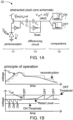
- Figure 1A is a schematic diagram of a DVS sensor 100 as disclosed in the above-referenced Lichsteiner document.
- the design comprises a fast-logarithmic photoreceptor circuit 101 coupled to a differencing circuit 103 that amplifies changes with high precision.
- An output of the differencing circuit 103 is supplied to a two-transistor comparator circuit 105.
- the indicated inverters are symbols for single-ended inverting amplifiers.
- the DC mismatch is removed by balancing the output of the differencing circuit to a reset level after the generation of an event.
- the gain of the change amplification is determined by the well-matched capacitor ratio C 1 / C 2 .
- the effect of comparator mismatch is reduced by the precise gain of the differencing circuit.
- the principle of operation of the DVS sensor 100 is depicted in Figure 1B .
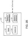
- Figure 2A is a block diagram of a low-power object detection/identification system 200 for authorizing performance of a device action.
- such actions include:
- the associated device is in some way associated with the system 200.
- vehicle locking mechanisms e.g., vehicle doors, vehicle engines
- home locking systems e.g., vehicle doors, vehicle engines
- workplace locking systems e.g., workplace entry authorization systems
- secure area authorization systems e.g., secure area authorization systems
- consumer appliance e.g., electronic device
- start and stop functions e.g., start and stop functions
- consumer device e.g., electronic device activation/deactivation functions.
- extended reality (XR) glasses with an image sensor can be employed as a sensing device, and the system 200 configured to recognize when a particular user and/or object is within a line of sight of the XR glasses.
- XR extended reality
- opening/activating locked items or devices is but one example out of many possible examples and is for purposes of illustration.
- other types of actions can be performed when the system 200 recognizes that a particular object or person is present, and all are contemplated to be within the scope of inventive embodiments.
- the system 200 comprises a camera module 201 that can include a standard Red Green Blue (RGB) Camera Image Sensor (CIS).
- RGB Red Green Blue
- CIS Camera Image Sensor
- cameras with different setups of color filters can instead be used if the use case is specific and only needs a specific set of colors.
- the camera module 201 can employ a monochrome camera using only one color or no color filter. In that case the threshold in the system (discussed later) would be a gradient of the specific color.
- the camera module 201 is coupled to a host system 202 that includes an Image Signal Processor (ISP) 203 that controls the camera module 201 down to subsets of its sensing capability. These subsets are herein called “sensing structures” and can be different in different embodiments. As non-limiting examples, a “sensing structure” can be any of the following:
- a sensing structure can also be associated with a particular color or set of colors.
- the ISP 203 that controls the camera module 201 is, in some embodiments, custom made to have specific characteristics for a specific use case.
- the host system 202 further includes an analyzer 205 that controls threshold levels that are used when deciding whether a sensed image sufficiently matches a given model.
- the analyzer 205 also decides what power level the system 200 should operate in.
- the host system 202 also includes a central processing unit (CPU) 207 for general-purpose calculations.
- CPU central processing unit
- the exemplary host system 202 also includes a Graphics Processing Unit (GPU) / Neural Processing Unit (NPU) 209 that is configured to run a neural network for detection and identification of sensed image features and compares these with one or more models of authorized objects/users.
- GPU Graphics Processing Unit
- NPU Neural Processing Unit
- identification can be accomplished by running state-of-the-art algorithms that are known to those of ordinary skill in the art.
- the exemplary host system 202 also includes a memory 211 for storing things such as, but not limited to, neural network weights, images, settings for hardware, and other needed software features.
- the camera module 201 comprises a sensor array 251 comprising a plurality of sensing structures that are configurable as will be discussed further with reference to Figure 4 .
- the camera module 201 further comprises a control unit 253 for controlling the various components of the camera module 201 in a way that conforms with the various actions described herein.
- the camera module 201 is able to make an initial conclusion whether an object or person being presented to the sensor module 251 is one of one or more previously authorized objects / persons, and to facilitate this function the camera module 201 includes a register 255 for users/objects.
- recognition of an object/person includes detecting whether a sufficient number of activated sensing structures are being triggered by the object/person being presented, and this means comparing the number of triggered sensing structures to a threshold. It is a purpose of the register 255 for users/objects to store settings for all of the objects/users that are available in a given model. There may be one or more than one such object/user.
- the initial conclusion made by the camera module 201 should be understood as being a sufficiently close match (within a defined threshold) between the results of the sensed data and the data stored in the register 255 per user/object or version of user/object, and the like.
- the initial conclusion is not made with 100% certainty. But finding an initial match provides sufficient confidence to warrant engaging a higher power stage of analysis that can be used to further enhance the detection and security of the detection with additional sensors or pixels to give higher resolution and the like.
- the system is able to expend only minimal energy in order to avoid having non-matching conditions constantly wake up the higher power system. The ratio of negative detections will likely always be much higher than positive results, thus resulting in significant power savings.
- the camera module 201 is able to detect when no object/user is being presented to the sensor module 251 and to remain in a very low power state under such circumstances, and then to be able to revert to a more active state when something (object/person) is then presented to the sensor module 251.
- this function involves tracking whether the sensor module 251 presently detects an image corresponding only to an image of an environmental background (i.e., an image without an object or person being presented to the sensor module 251). So long as only background is detected, the camera module 201 can remain in the very low power state. If a sufficient enough change to the scanned image is detected, the more active state is entered.
- the camera module 201 further includes a register 257 for a background image. It is a purpose of the register 257 for background to store settings for a background that is available in a given model.
- Figure 3 is a schematic / state diagram illustrating the concept of a multi-stage authorization / activation process.
- Processing effort begins at a minimal level, depicted as the smallest circle in the left-most position in the diagram, which represents a lowest-power processing state 301.
- Embodiments consistent with the invention such as but not limited to the exemplary system 200 of Figure 2 , perform the processing of at least state 301.
- a baseline model selects a first number of sensing structures of the camera image sensor 251, with the number being less than a total number of sensing structures of the camera image sensor 251.
- the baseline model is configured to detect a very small number of key image features that would be expected to be found in an image of an authorized object/user, and the first number of sensing structures is selected to be able to detect this small number of key image features.
- the number of stages performed before a final conclusion is reached is implementation dependent.
- four states 301, 303, 305, and 307 are shown. But in other embodiments there could be more or fewer states, each associated with a different amount of processing effort to detect whether a sensed image matches a model of an authorized object/user.
- An advantage of this multi-stage testing arrangement is that, at the conclusion of processing, the system is able to detect, with as little energy consumption as possible, whether a known object/user has been identified, and this reduction in energy consumption enables the system to employ an always-on camera.
- the camera module 201 It is advantageous to have the lowest level of power handled in the camera module 201 itself.
- Self-contained hardware embodiments of the camera module 201 can be configured for this purpose in order to enable a low-power, always-on embodiment.
- Based on the baseline signature a few lines of the CIS 251 will be active. For example, suppose a user has a green shirt and blue trousers at the time of using the system 200. The system 200 adds these important colors to the model during a model updating phase of processing.
- the camera module 201 is activated accordingly.
- green pixels in a few rows are activated at the top of the CIS 251 (above the center of the vertical field of view for example) and blue pixels are activated in the bottom of the CIS 251 (below the center of the vertical field of view for example).
- the pixel rows that are active indicate a triggering event once a threshold of pixel value is found.
- the algorithm used to analyze the selected set of pixels is also robust enough to manage a range of values that can identify a certain pattern but with alignment towards the sensor somewhat askew. In the example it can be one of many situations affecting the intensity of certain colors for example slightly lower, to the side or further away. This could be done on sensor level of the camera module 201 or in the ISP 203 running in low power mode.
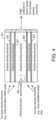
- a "sensing structure” is considered to be a row of pixels, and four of these are shown in an activated state: a first sensing structure 403 for detecting blue; a second sensing structure 405, also for detecting blue; a third sensing structure 407 for detecting green; and a fourth sensing structure 409, also for detecting green.
- these selections are for purposes of illustration only; there is no particular significance to the number of illustrated sensing structures, their locations or orientations within the array 401, the particular colors being sensed, or even the fact that pixels are selected to form a contiguous portion (e.g., a row) of the array 401.
- the schematically depicted sensing structure 420 is included in the figure to represent sensing structures in the "general case".
- Remaining sensing structures illustrated in Figure 4 are, in the illustration, inactive.
- a next level of identification could, for purposes of example, be that 2/3 of the Vertical Field of View (VFOV) starting at the top looks at green and 2/3 of the VFOV starting from the bottom looks at blue.
- the question being asked could be, for example, is it possible to identify a green shirt and blue trousers? If yes and the image obtained from the further activated sensing structures sufficiently matches this level's model, then processing moves on to a next power level; otherwise processing reverts back to an adaptive identification sleep mode.
- the identification processing can be performed by the neural processing unit 209 and the analyzer 205 can be used to decide whether testing at the next power level should be activated or instead whether the current (higher) power level should be deactivated based on the result of the neural network.
- a third level of testing can be that the full FOV is activated with all colors but at a lower resolution, for example 1MP instead of 8MP (if that is the maximum resolution of the camera module 201).
- the image is again sent to the neural processing unit 209 and the analyzer 205, this time with a different set of weights. Testing can, for example, look to see whether a person and a face can be recognized; if so, the analyzer 205 will decide to go to the next power level.
- an image with full 8MP resolution will be taken.
- the ISP 203 will crop the face and/or other biometrical attributes and send the information to the neural processing unit 209 and the analyzer 205 for identification. If the imaged person is identified as a user, the item or device will be triggered to open / unlock depending on the use case.
- the full system can be further configured to turn on and provide the image to a more capable processor for identification/analysis.
- the more capable processor can be configured to be nearby the camera module 203 (e.g., disposed within the host system 202 as illustrated in Figure 2A ), or alternatively it can be a central computing resource (e.g., server, mobile edge cloud, etc.).
- any particular embodiment depends on a number of factors, including whether the low-power system is to be a stand-alone system, or whether it is part of a larger system of sensors and gates - in the latter, an updated profile might need to be shared with the other sensor nodes.
- a local application processor is assumed, since it would be the natural system implementation (there should be a CPU with an ISP and some image processing in the form of accelerator/GPU/NPU). But it will be noted that, for example, the final one or two steps 305, 307 of processing (see Figure 3 ) can be performed in a system that is not local to the system 200, so that communication between the sensor system and the more capable device is needed.
- the change from one of the power-saving states to the full system being on can be done from any of the power levels.
- One trigger of this could be that when a person stands sufficiently close to the associated device (e.g., car), at least a certain number of horizontal pixels will be filled and that will trigger the full system. Other triggers are also possible.
- Figure 5 is a flowchart of actions performed by the system 200 in accordance with a number of embodiments.
- the blocks depicted in Figure 5 can also be considered to represent means 500 (e.g., hardwired or programmable circuitry or other processing means) for carrying out the described actions.
- the system 200 Before the system 200 can recognize a particular object/user, it must first perform initializing actions that include taking baseline measurements (step 501) of the object/user and calculating what sensor settings (e.g., which sensing structures 420 should be activated) for lowest power mode recognition of a particular object/user (step 503). At the conclusion of the initializing actions, the system 200 is ready to recognize the particular object/user when that object/user is detectable by the camera module 203.
- initializing actions include taking baseline measurements (step 501) of the object/user and calculating what sensor settings (e.g., which sensing structures 420 should be activated) for lowest power mode recognition of a particular object/user (step 503).
- the system 200 is ready to recognize the particular object/user when that object/user is detectable by the camera module 203.
- the system 200 is in an adaptive identification sleep mode (step 505) that consumes a lowest amount of energy.
- the system 200 can be configured to detect when an object/user is being presented to the camera module 201 and in response to the detection, to use a previously generated baseline model of an authorized object/user to select and activate a lowest number of sensing structures 420.
- the system 200 can be configured to be always-on with a lowest number of sensing structures 420 always selected and activated so that an authorized object/user can be immediately recognized when presented to the camera module 201. In this alternative, there is no need to detect that an object/user has come within view of the camera module 201.
- a scanning step 507 signals from the active sensing structures 420 are compared with the baseline model (e.g., by comparing the strength of the signals to a threshold) (decision block 509). If the comparison fails ("No" path out of decision block 509) then the system 200 remains in the lowest power state and processing in some embodiments reverts back to step 507.
- the system 200 can be further configured to handle situations in which an object or user that should be recognized is, for some reason, not recognized.
- the system 200 can be further configured to include a mechanism that allows the user to override the low power operation and force the system to transition to a higher-power analysis that would then more accurately decide whether the object/person is recognized. For example, as shown in Figure 5 , upon failing to recognize the object/user at decision block 509, the system 200 can test to determine whether an override operation has been triggered (decision block 510).
- An override operation can be triggered by an action such as the user pressing a button, or gripping a doorknob. The particular form of such triggering is not essential to inventive embodiments. If no override is detected ("No" path out of decision block 510), then processing continues to step 507 as discussed above. But if an override has been triggered ("Yes" path out of decision block 510), then higher level processing is invoked to provide a more reliable (and more power consuming) analysis. In some embodiments, this involves sending information about the failed scan to a host system 202 or other higher level processor for analysis (step 511), the host system (or other) processor performing the higher level analysis (step 513) and performing another test against a threshold (decision block 515).
- step 519 is reached if the initial comparison of the signals from the active sensing structures 420 with the baseline model passed ("Yes" path out of decision block 509).
- Successfully passing the lowest level testing means that the system is now willing to expend more energy to determine with greater accuracy whether the object/user presented to the camera module 201 is actually an authorized object/user.
- a next (increased) number of sensing structures 420 is activated (step 519), a comparison of the activated sensor signals with a baseline measurement is made (step 523) (e.g., by processing elements of the host system 202), and the comparison result is compared with a predetermined threshold value (decision block 525).
- step 511 If the comparison result is greater than or equal to the predetermined threshold value ("Yes" path out of decision block 525) the object/person was again recognized by this next level of processing, so to provide even greater accuracy processing continues to step 511 and further actions are taken as described above. As previously discussed, this involves performing an even higher-level analysis by the host system 202 or other processing system that is more capable but also more energy demanding than what is done in the camera module 201.
- actions may further include adjusting the predetermined threshold value and/or other hysteresis-related parameters), deactivating the host system 202 (if it had been activated) and returning to a lowest level of energy consumption operation at step 507.
- Figure 6 is a flowchart of actions taken by the system 200 in accordance with a number of embodiments.
- the blocks depicted in Figure 6 can also be considered to represent means 600 (e.g., hardwired or programmable circuitry or other processing means) for carrying out the described actions.
- Figure 6 focuses on actions taken as part of system initialization. As mentioned above, during operation the system 200 relies on one or more baseline models which specify key image features that should be looked for during each stage of authorization processing. Figure 6 focuses on aspects relating to the creation and updating of a baseline model.
- An initial test decides whether the camera module 201 is presently imaging an object/user that it has decided is an approved object/user (decision block 601). This decision can be made by, for example, taking actions such as those described above with respect to Figure 5 .
- a picture of the object/user is obtained (e.g., a high resolution image) (step 603) and features from the obtained image are compared with corresponding features of the stored model to produce a set of calculated differences and the model is updated accordingly (step 605).
- Predefined threshold levels that are used during the authorization process e.g., refer to Figure 5
- power levels are adapted based on the updated information (step 607) and these are stored as well.
- the system 200 can continue to take more pictures and update the model accordingly, although this is not an essential aspect of this feature.
- the model has been updated and system operation begins at the lowest energy consumption level (step 611).
- a device associated with the system 100 is also put into a locked/deactivated state (step 613).
- decision block 601 if the object/user presently in front of the camera module 201 is not recognized as an approved object/user ("No" path out of decision block 601) then the question is whether this object/user is an authorized one for which a baseline model should be created. One way of testing this is detecting whether an authorization token is being presented to the system (decision block 615). If not ("No" path out of decision block 615) then the device associated with the system 200 should be maintained in a locked/deactivated state (step 617).
- a baseline model should be built at this time ("Yes" path out of decision block 619), then some number of pictures (the exact number depends on the particular algorithm being used) are taken of the object/user, important features extracted from those pictures, and the resultant model (e.g., a two- or three-dimensional model) built (step 623). It is advantageous to calculate the model using a higher-level (e.g., highest level) processing capability, since model building is a power- and processing-intensive activity.
- the model is then stored so that it can be ready for use (step 625) and processing proceeds to step 607 in which parameters of the system 200 are initialized for use at each of the different power levels. Further processing continues as already described above.
- Figures 7A and 7B which, in one respect, are in combination a flowchart of actions taken by the system 200 in accordance with a number of embodiments.
- the blocks depicted in Figures 7A and 7B can also be considered to represent means 700 (e.g., hardwired or programmable circuitry or other processing means) for carrying out the described actions in order to authorize activation of, for example, devices associated with (e.g., by means of proximity) the system 200.
- means 700 e.g., hardwired or programmable circuitry or other processing means
- the strategy adopted in the illustrated embodiment involves, loading the one or more latest models of known users (step 701) and for each user, calculating pixel values that will be used in the low power state (step 703). Before the low power mode of the camera module 201 is activated, the calculated settings are loaded into the user/object register 255 (step 705), and these loaded settings will set the thresholds for all colors and the number of rows that are active for each user.
- the user/object register 255 has room for at least one user.
- the background model is calculated (step 707) every time just before the low power mode of the sensor is activated. From the background model, pixel values and thresholds for colors and number of sensing structures 420 (e.g., rows of pixels) that will be actively scanned are calculated (step 709) and loaded into the background register 257 (step 711).
- the sensor goes into low power mode (step 713).
- low power mode each user setting is scanned one after another.
- the background setting is also scanned as a last step. If the signal from the sensor is over or under a set threshold a trigger is sent to the host.
- the sensor 251, 401 is scanned based on the loaded user setup (step 715).
- the output from the sensor 401 is compared to the loaded threshold value (decision block 717), and if the comparison passes (e.g., is greater than or equal to the threshold) ("Yes" path out of decision block 717), then the host system 202 is triggered/activated (step 719) to further process a scanned image to decide, with better accuracy, whether the object/user presented at the sensor 401 is recognized.
- This higher level processing may, in some embodiments, comprise several levels of ever higher level processing, as described above.
- processing determines whether the last object/user in the list of known objects/users has been checked (decision block 721). If not ("No" path out of decision block 721), settings for the next object/user in the list are loaded into the camera module 201 (step 723), processing reverts back to step 715 for further testing.
- the sensor is scanned using the loaded settings for the background (step 725).
- the strategy assumes that, so long as no object or person is presented to the camera module 201, it should be “seeing” only the background, and its output should accordingly be more or less constant over time (within some tolerance level, determined based on application).
- the strategy allows for some level of background deviation since, for example, people may be walking by the sensor without presenting themselves, lighting conditions can change over time, and the like. Therefore, with the background settings in effect, the sensor output is checked against its corresponding threshold level (decision block 727) to see whether or not it is stable.
- step 727 If the sensor output is within some predetermined margin of the threshold ("Yes" path out of decision block 727) then no significant change has been detected. To avoid the possibility that the system 200 might miss the appearance of an object or person being presented to the camera module 201, the effective system settings are changed to be those of the first user in the list (step 729) and processing reverts to step 715 and proceeds as discussed above.
- the host system 202 is activated/triggered (step 719) to further process a scanned image to decide, with better accuracy, whether the object/user presented at the sensor 251, 401 is recognized.
- This higher level processing may, in some embodiments, comprise several levels of ever higher level processing, as described above. It is recognized that this may lead to more activations of the higher-power consuming system, but being able to recognize a user even when some changes in appearance have been made justify this action.
- reference letters may be provided in some instances (e.g., in the claims and summary) to facilitate identification of various steps and/or elements. However, the use of reference letters is not intended to impute or suggest that the so-referenced steps and/or elements are to be performed or operated in any particular order.
- the technology is an optical sensor module having a controller, a sensor array, present state decision circuitry, and a pattern recognizer.
- the sensor array comprises a plurality of CMOS sensor pixels, wherein the sensor array is configured to supply one of a plurality of analog sensor signals at each of a sequence of sample times, wherein at each of the sample times, the one of the plurality of analog sensor signals is derived from one or more of the plurality of CMOS sensor pixels.
- the present state decision circuitry is configured to compare the one of the plurality of the analog sensor signals for each of the sequence of sample times with a respective controller-selected reference voltage and to generate therefrom a respective single state decision signal.
- the pattern recognizer is configured to assert a pattern recognition signal whenever a plurality of sequentially generated single state decision signals matches a currently active one of a set of one or more reference sequences of single state decision signals.
- the controller is configured to assert a host system trigger signal when the pattern recognition signal is asserted a predefined number of times in sequence.
- At least one of said one of the plurality of analog sensor signals is an analog sensor signal representing an output from a single one of the plurality of CMOS sensor pixels.
- At least one of said one of the analog sensor signals is a binned analog sensor signal produced by two or more of the plurality of CMOS sensor pixels.
- the set of one or more reference sequences includes at least two reference sequences of single decision signals; a first one of the set of one or more reference sequences differs from a second one of the set of one or more reference sequences; a first assertion of the pattern recognition signal occurs at a first time whenever the plurality of sequentially generated single state decision signals matches the first one of the set of one or more reference sequences; a second assertion of the pattern recognition signal occurs at a sequentially second time whenever the plurality of sequentially generated single state decision signals matches the second one of the set of one or more reference sequences; and the controller is configured to assert the host system trigger signal whenever the pattern recognition signal is asserted at both the first and second times.
- the optical sensor module further comprises a voltage multiplexor that selects the controller-selected reference voltage from a plurality of reference voltages, wherein the controller is configured to select the controller-selected reference voltage based on profile information stored in a register.
- the optical sensor module further comprises one or more Dynamic Vision Sensor, DVS, sensor pixels that collectively assert a DVS trigger signal when luminance detected by at least one of the one or more DVS sensor pixels changes by a threshold amount.
- DVS Dynamic Vision Sensor
- the controller is configured to:
- operation in the low power mode comprises activating at least one but fewer than all of the CMOS sensor pixels.
- the controller is configured to increase a number of activated CMOS sensor pixels when the host system trigger signal is asserted.
- the present state decision circuitry further comprises circuitry configured to invert a polarity of the single state decision signal.
- the optical sensor module (801, 1301) is comprised in a mobile communication device.
- the optical sensor module (801, 1301) is comprised in a low-power sensor device.
- circuitry configured to perform one or more described actions is used herein to refer to any such embodiment (i.e., one or more specialized circuits alone, one or more programmed processors, or any combination of these).
- the invention can additionally be considered to be embodied entirely within any form of nontransitory computer readable carrier, such as solid-state memory, magnetic disk, or optical disk containing an appropriate set of computer instructions that would cause a processor to carry out the techniques described herein.
- nontransitory computer readable carrier such as solid-state memory, magnetic disk, or optical disk containing an appropriate set of computer instructions that would cause a processor to carry out the techniques described herein.
- the various aspects of the invention may be embodied in many different forms, and all such forms are contemplated to be within the scope of the invention.
- any such form of embodiments as described above may be referred to herein as "logic configured to” perform a described action, or alternatively as “logic that" performs a described action.
- An aspect of the herein-described technology pertains a highly optimized sensor design and mechanisms that are suitable for the initial stages of object analyses for a system that can be always-on.
- the system design utilizes a multi-stage approach in which decisions made at the lowest level of analysis or triggering mechanism have the least confidence but are made with minimal power consumption.
- a positive triggering at that lowest stage leads to a subsequent stage of a (perhaps slightly) more complex analysis - one that is still far below the level of complexity (and power consumption) associated with a host system involving CPUs, GPUs, or NPUs as well as data communication between chips.
- the first level of detection is produced by a sensor having a sparse matrix of DVS (Dynamic Vision Sensor) pixels embedded in an otherwise conventional CMOS matrix. Additional circuitry is provided to enable operation in which the CMOS matrix remains inactive while the DVS pixels detect changes. When enough such pixels indicate a change above a certain threshold, a triggering signal is generated indicating that something fundamental has changed in the image.
- the trigger from the DVS mechanisms causes the mode of operation to change from the lowest level to a second ultra-low power mode in which a subset of the CMOS array is activated. This subset operates in conjunction with analog circuitry as well as simple state machines that, together, enable analysis of the sensed color patterns at a very low level of power consumption.
- the second ultra-low power mode mechanism is able to test the sensed image against a limited set of user profiles, thereby allowing this stage to trigger (i.e., indicate a match) based on different possible patterns.
- the senor can be put into a more normal mode, or a previously known sub-array mode, for a more in-depth analysis of camera content in, for example, a host processor in the device.
- This type of mode consumes much more energy but comes with the benefit of higher confidence in the decisions being made.
- Several different options for implementing the higher-level analysis are generally known, and it is beyond the scope of this invention to describe these in detail.
- FIG. 8 it is a block diagram of a system including an always-on sensor module 801 coupled to a host system 803 such as, but not limited to, the exemplary host system 202 described earlier.
- the sensor module 801 comprises a sensor array 851 comprising a plurality of sensing structures that are configurable as was discussed earlier with reference to Figure 4 .
- the sensor array 851 is further populated with some number of DVS pixels (i.e., in addition to the CMOS pixels), this being for enabling ultra-low always on features as will be further described below.
- the sensor module 801 further comprises a control unit 853 for controlling the various components of the sensor module 801 in a way that conforms with the various actions described herein.
- the sensor module 801 is able to make an initial conclusion whether an object or person being presented to the sensor array 851 is one of one or more previously authorized objects / persons, and to facilitate this function the sensor module 801 includes a register 255 for users/objects.
- recognition of an object/person includes detecting whether a sufficient number of activated sensing structures are being triggered by the object/person being presented, and this means comparing the number of triggered sensing structures to a threshold. It is a purpose of the register 255 for users/objects to store settings for all of the objects/users that are available in a given model. There may be one or more than one such object/user.
- the initial conclusion made by the sensor module 801 should be understood as being a sufficiently close match (within a defined threshold) between the results of the sensed data and the data stored in the register 255 per user/object or version of user/object, and the like.
- the initial conclusion is not made with 100% certainty. But finding an initial match provides sufficient confidence to warrant engaging a higher power stage of analysis that can be used to further enhance the detection and security of the detection with additional sensors or pixels to give higher resolution and the like.
- the system is able to expend only minimal energy in order to avoid having non-matching conditions constantly wake up the higher power system. The ratio of negative detections will likely always be much higher than positive results, thus resulting in significant power savings.
- the sensor module 801 is able to detect when no object/user is being presented to the sensor array 851 and to remain in a very low (or in some embodiments, an ultra-low) power state under such circumstances, and then to be able to revert to a more active state when something (object/person) is then presented to the sensor array 851.
- This function involves tracking whether the sensor array 851 presently detects an image corresponding only to an image of an environmental background (i.e., an image without an object or person being presented to the sensor array 851). So long as only background is detected, the sensor module 801 can remain in the very (or ultra) low power state. If a sufficient enough change to the scanned image is detected, the more active state is entered.
- the sensor module 801 further includes a register 257 for a background image. It is a purpose of the background image register 257 to store settings for a background that is available in a given model.
- the exemplary sensor module 801 further includes:
- the sensor module 801 supplies an image to the host system 803 for it to undergo a more computationally complex analysis once an object has been detected using the lower-power detection strategies of the sensor module 801 itself.
- always-on operation is facilitated by utilizing a sensor array 851 populated with both CMOS sensor (pixel) elements and DVS sensor (pixel) elements.
- the CMOS sensor elements are further configured to be dynamically configurable such that only selected ones are activated, based on what level of sensor resolution is desired. Power savings are achieved because only the activated sensor elements expend energy.
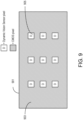
- FIG. 9 is a diagram of a non-limiting example of a sensor array 901.
- the sensor array 901 comprises a plurality of CMOS sensor pixels 903 (illustrated by diagonal shading), and also one or more DVS sensor pixels 905 (each one of the sensors denoted by "D").
- CMOS sensor pixels 903 Illustrated by diagonal shading
- DVS sensor pixels 905 each one of the sensors denoted by "D"
- the CMOS sensor pixels 903 are activated.
- the DVS sensor pixels 905 are relied on exclusively for the purpose of detecting changes in luminescence. Such changes are taken as an indication that some person/object has come into view of the sensor array 901, requiring that a next higher level of processing be activated to determine whether the person/object is recognized.
- the DVS sensor pixels 905 serve only to indicate the presence or absence of an object in front of the sensor array 901, there need not be many of them. In the example, there are only a few DVS sensor pixels 905 spread out over the sensor array 901 to cover the field of view of the camera, thus being able to detect changes in luminescence over a larger area. Since the DVS sensor pixels 905 occupy positions that would otherwise hold CMOS sensor pixels, the image data from the "missing" CMOS sensor pixels can be calculated / estimated from data provided by neighboring conventional pixels. This may possibly produce some artifacts in those areas. The calculations involved in providing the missing data are the same as calculations known by those of ordinary skill in the art for compensating for defective pixels on a sensor. There are a number of well-known algorithms for accomplishing this, such as nearest neighbor calculations, bi-linear interpolation, linear interpolation, and the like. A complete description of such known algorithms is beyond the scope of this disclosure.
- a pixel 903 must be pre-charged before it can detect light. Once pre-charged, the pixel 903 detects any input light. The detected light is output when the pixel 903 is driven.
- each pixel 903 of the sensor array 901 is controlled by a RESET signal, which selectively connects the pixel 903 to a voltage level, V RST , to pre-charge the pixel to enable the pixel to capture light; and a separate DRIVE signal, which selectively connects the pixel 903 to a voltage level, V DD , to drive the pre-charged pixel 903 to enable the pixel 903 to output the detected light.
- Figure 10B shows a more detailed example of an exemplary pixel 903 comprising multiple transistors and a diode. It will be appreciated that implementations other than the one shown in Figure 10B may be used for the pixel 903 of Figure 10A .
- Exemplary pixels include, but are not limited to, Front Side Illuminated (FSI) pixels and Backs Side Illuminated (BSI) pixels. It will be appreciated that the structure of BSI pixels enables wiring to be added without impacting the aperture ratio of the pixel, and thus enables implementation of the solution presented herein without reducing the aperture ratio of the pixel.
- FSI Front Side Illuminated
- BSI Backs Side Illuminated
- the dynamically configurable array of CMOS sensor pixels 903 provides a mechanism for controlling the analog domain power consumption of the system by controlling how many and which pixels 903 are pre-charged. As such, the solution reduces the power consumption of the sensor array 901 by an amount proportional to the uncharged pixels 903. For example, if only half of the pixels 903 are pre-charged, the analog power consumption is reduced by approximately 50%. It will be appreciated that only those pixels that are pre-charged are driven. As such, in some embodiments, the pre-charging and driving aspects of the pixels 903 may be coordinated, e.g., by the control unit 853 and/or by any charge control/drive circuits.
- FIG. 10C shows a block diagram of an exemplary sensor array 1000.
- Image sensor array 1000 comprises a sensor array 1010 comprising a plurality of CMOS sensor pixels 903 (the DVS sensor pixels 905 (which are also present as discussed above) are ignored for purposes of this discussion), a charge control circuit 1020, and a drive control circuit 1030.
- the sensor array 1010 comprises two or more sensor segments 1014, where each of the two or more sensor segments 1014 comprises a different set of pixel(s) 903. While sensor array 1010 is shown as a two-dimensional matrix of pixels 903, it will be appreciated that the sensor array 1010 may alternatively comprise a vector of pixels 903, where the vector of pixels 903 comprises two or more sensor segments 1014.
- the charge control circuit 1020 is configured to pre-charge pixels 1012 via RESET control lines, while the drive control circuit 1030 is configured to drive pre-charged pixels 1012 via DRIVE control lines. While Figure 10 shows separate RESET and DRIVE control lines for each of three sensor segments 1014a-c, it will be appreciated that each segment-specific RESET and/or DRIVE control line may represent individual RESET and DRIVE control lines for each pixel 903 in the corresponding segment 1014, or may represent a common RESET and/or DRIVE control line specific to the corresponding segment 1014. Further, it will be appreciated that the solution presented herein does not require three sensor segments 1014a-c as shown in Figure 10C ; sensor array 1010 may comprise fewer or additional sensor segments 1014 than those shown.
- the senor is able to cope with different environmental illumination levels and shifts by adjusting the white balance and exposure level based on a rolling average of the pixels 903 that are scanned during the low power mode.
- the white balance and exposure levels are fed back to the control unit 853 which responds by adjusting the trigger levels by amounts that depend on the measured environment illumination.
- the sensor readout can be configured to operate in any of a number of different modes, each associated with a correspondingly different pattern. This enables easy and power efficient readout from the pixels 903. In the different modes, the output from pixels 903 in the selected area are averaged in the analog domain before being sent to an A/D converter, a comparator and a pattern recognizer (all discussed further below).
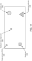
- Figure 11 illustrates a number of exemplary pixel readout modes. It will be appreciated that other modes, not illustrated, are also possible. The illustrated modes are:
- Figure 12 depicts an example of how a binning can be performed and support different shapes.
- a 4x4 pixel array is shown to illustrate the point, but embodiments consistent with the invention are not limited to this particular arrangement.
- Three different binning options are supported in this example: a top triangle portion "a" 1201; a bottom triangle portion "b" 1203; and a square 1205 formed by combining the top and bottom triangle portions 1201, 1203.
- To support more complex shapes more readouts have to be done and matched in the pattern recognizer.
- the sensor module 801 also includes analog circuitry capable of making a coarse decision about whether an image is recognized or not while consuming very low amounts of energy.
- analog circuitry capable of making a coarse decision about whether an image is recognized or not while consuming very low amounts of energy.
- An exemplary embodiment of such circuity is illustrated in Figure 13 .
- the circuitry 1300 can be conceptually divided into two parts: an A/D converter that is used in an image sensor system such as is found in the host system 803; and additional, simple circuitry for performing the low power object identification step.
- An A/D converter that is used in an image sensor system such as is found in the host system 803
- additional, simple circuitry for performing the low power object identification step.
- the example shown in Figure 13 employs a full multi-bit A/D converter 855 whose multi-bit digital output signal enables image analysis requiring higher levels of image resolution (e.g., some number, X, bits).
- the digital output of the X-bit A/D converter 855 can be provided to the host system 803 as shown in Figure 8 .
- the X-bit A/D converter 855 receives an analog signal 1301 from the sensor array 901, and also receives reference voltages 1303 against which the analog signal 1301 is compared, as is known in the art of analog-to-digital signal conversion.
- the additional, simple circuitry for performing the low power object identification step in this exemplary embodiment includes a voltage multiplexor 857, a present state decision circuit 859, and pattern recognition circuitry (e.g., a state machine) 861.
- the present state decision circuit 859 can, in its simplest form, be a 1-bit comparator 1305 that compares the received analog signal 1301 from the sensor array 851 with a reference voltage set to an object-dependent decision threshold 1315 to produce a 1-bit comparison result signal 1311 having either a binary 0 or 1 value, depending on the results of the comparison. Production of a positive comparison result by the comparator 1305 is taken as an indication that an object in front of the CMOS sensor pixel 903 array may have been recognized.
- the decision threshold 1315 is selected from one of the reference voltages 1303 that are already available for the high power A/D converter 855. This is not an essential aspect of the technology; to the contrary, a decision threshold voltage can, in other embodiments, be generated from any other source.
- selection is performed by the voltage (or power) multiplexor 857 having a selection control signal supplied by the control unit 853.
- the control unit 853 bases selection on whichever object profile is active at any given moment, and in particular bases selection on profile-related values stored in the registers for users/objects 255 and registers for background 257 as shown in Figure 8 .
- the voltage multiplexor 857 is capable of supporting all voltages from the high power A/D converter; in other embodiments, only a subset of the available voltages.
- the exemplary comparator 1305 asserts the comparison result signal 1311 (e.g., from low to high) when a positive comparison is made between the received analog signal 1301 and the object-dependent decision threshold 1315 but in some instances, it may be desirable in the low-power mode to detect when an analog signal 1301 is not greater than or equal to a reference voltage (i.e., to detect transitions from high to low instead of from low to high), and for this purpose in some but not necessarily all embodiments the circuitry 1300 is further equipped with logic circuitry, such as an Exclusive OR (XOR) gate 1307, that performs a logical Exclusive OR between the 1-bit comparison result signal 1311 from the comparator 1305 and a decision polarity signal 1309 generated by the control unit 853.
- XOR Exclusive OR
- the 1-bit digital comparison result signal 1311 passes through unchanged; when the decision polarity signal 1309 is high, the 1-bit digital comparison result signal 1311 passes through in an inverted form.
- the output of the XOR gate 1307 is herein denoted single state decision signal 1313.
- the control unit 853 therefore receives a DVS trigger signal 1319 that is asserted when the DVS sensor pixels 905 detect a change in luminosity. Assertion of the trigger signal 1319 causes the control unit 853 to transition the unit from ultra-low power mode into the (higher level) low power mode.
- the sensor module 901 includes a state machine or pattern recognizer 861.
- the pattern recognizer receives the single state decision signal 1313, which represents a comparison decision based on sensor output from any of the above-described sensor operational modes.
- the pattern recognizer 861 expands the low-power image analysis capability by freeing it from having to make decisions based on only a single, instantaneous sensor output value.
- an unbroken string of assertions does not mean that the same pattern has been detected over a stretch of time; one assertion can mean for example that a triangle of a particular luminance has been detected, and a next assertion can mean for example that a blue circle has been detected.
- FIG. 14 illustrates a state machine 861 for this example. As can be seen in the figure, transitions are made from a first state to a second, then to a third, and so on for some number, n, states, so long as each next transition indicates that a sensor output satisfied a particular threshold value.
- a pattern recognition decision signal 1321 is, in some embodiments, routed back to the controller 853.
- the controller 853 is configured to assert a host system trigger signal 1323 when the pattern recognition signal 1321 is asserted. Assertion of the host system trigger signal 1323 can, for example, cause an affiliated host system 803 to become activated and accordingly perform a higher-level of object recognition analysis.
- the controller 853 is configured to increase a number of activated CMOS sensor pixels 903 when the pattern recognition signal 1321 is asserted. This serves to provide a higher resolution image capture in support of the host system's higher-level of object recognition analysis.
- the pattern recognizer / state machine 861 can take on any of a number of different forms depending on what the designer would like to use as a trigger scheme. For example, several different state machines could be provided in a design, with the active one being chosen by the control unit 853; the control unit 853 gets state machine selection information from the settings loaded into the register for users/objects 255 and register for background 257.
- the system is able to detect a wider range of different complex patterns by having several different pattern recognizers 861. It can also be that several complex patterns need to be recognized before the host is triggered. This is controlled by the control unit 853 that get this information from the register settings for each profile that is present in the system.
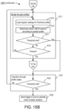
- Figures 15A and 15B depict a flowchart of actions performed by the system sensor module 801 in accordance with a number of embodiments.
- the blocks depicted in Figures 15A and 15B can also be considered to represent means 1500 (e.g., hardwired or programmable circuitry or other processing means) for carrying out the described actions.
- the process includes loading the different object/user/background profiles into the respective register settings of the sensor module 801 (step 1501). These are the user register settings, object register settings, and background register settings produced at, for example, steps 501 and 503 (see Figure 5 ).
- the sensor module 801 is then placed into an ultra-low power mode, in which only the DVS pixels 905 are active (step 1503).
- the DVS pixels 905 operate asynchronously, and include circuitry that issues a trigger when an illumination difference is detected according to the DVS pixel setting (step 1505).
- the system remains in ultra-low power mode so long as the DVS pixels 905 do not issue a trigger signal 1319 ("No" path out of decision block 1507).
- the system transitions to the low power mode in which the CMOS sensor pixels 903 are started (step 1509).
- the system iterates through all of the object/user profiles to see if CMOS sensor outputs match any of them (step 1511). More particularly, register settings are loaded for initially a first and then (if warranted) a next profile (step 1513), and the CMOS sensor pixels 903 are selectively activated according to the loaded register settings (step 1515).
- step 1517 If the threshold specified by the loaded profile settings are not satisfied ("No" path out of decision block 1517), a further test is performed to determine whether a timeout condition has been satisfied (decision block 1519). If it has ("Yes" path out of decision block 1519), processing reverts back to step 1503, where the system is switched back into ultra-low power mode.
- a strategy is adopted in which all profiles are checked some predetermined number (one or more) of times and if so, processing reverts back to step 1503.
- processing reverts back to step 1513 where settings from a next profile are loaded into the registers and iteration continues for another round.
- step 1521 a pattern of successively generated output signals from the CMOS sensor pixels 903 are tested against a predefined pattern for the current profile. Each generated CMOS sensor output is tested against a corresponding next predefined state condition (decision block 1523) (see, e.g., Figure 14 ). If at any point the threshold condition is not satisfied ("No" path out of decision block 1523), then a match has not been found and processing reverts to step 1511 where iteration through the profiles is taken up again.
- a trigger is generated and sent to the host system 803 (step 1525) so that a higher-resolution analysis can be performed by that unit as described earlier.
- FIG. 16 illustrates an exemplary controller 1601 of a sensor module 801 in accordance with some but not necessarily all exemplary embodiments consistent with the invention.
- the controller 1601 includes circuitry configured to carry out any one or any combination of the various functions described above.
- Such circuitry could, for example, be entirely hard-wired circuitry (e.g., one or more Application Specific Integrated Circuits - "ASICs").
- programmable circuitry comprising a processor 1603 coupled to one or more memory devices 1605 (e.g., Random Access Memory, Magnetic Disc Drives, Optical Disk Drives, Read Only Memory, etc.) and to an interface 1607 that enables bidirectional communication with other elements of the sensor module 801.
- the memory device(s) 1605 store program means 1609 (e.g., a set of processor instructions) configured to cause the processor 1603 to control other system elements so as to carry out any of the aspects described above.
- the memory device(s) 1605 may also store data (not shown) representing various constant and variable parameters as may be needed by the processor 1603 and/or as may be generated when carrying out its functions such as those specified by the program means 1609.
- Various embodiments consistent with the invention provide an advantage over conventional technology in that a first level of object detection can be done at extremely low power consumption enabling the use in always-on battery-operated devices.
- DVS sensor pixels 905 especially enable always-on operation, since the next higher level of processing (at a higher level of power consumption) is invoked only when actually needed.
- CMOS sensor pixels 903 use of analog circuitry and selective activation of CMOS sensor pixels 903 to perform a low-level of image analysis in turn ensures that higher levels of processing power are not invoked unless they are actually needed.
- Embodiments consistent with the invention may be deployed in a number of different kinds of devices.
- low power, always-on sensor technology can advantageously be used in any number of battery-powered devices, such as mobile communication devices (e.g., User Equipment - "UE"). It is also well-suited for use in low-power devices such as Internet-of-Things (IoT) devices.
- IoT Internet-of-Things
- Such devices may themselves be sensor devices for sensing and reporting other aspects of an environment (e.g., temperature, movement, etc.)
Landscapes
- Engineering & Computer Science (AREA)
- Multimedia (AREA)
- Signal Processing (AREA)
- Software Systems (AREA)
- Studio Devices (AREA)
- Image Analysis (AREA)
- Image Processing (AREA)
Claims (15)
- Module de capteur optique (801), comprenant :un dispositif de commande (853) ;un réseau de capteurs (851, 901) comprenant une pluralité de pixels de capteur CMOS (903), dans lequel le réseau de capteurs (851, 901) est configuré pour fournir un signal de capteur analogique d'une pluralité de signaux de capteur analogiques (1301) à chaque temps d'échantillonnage d'une séquence de temps d'échantillonnage, dans lequel, à chacun des temps d'échantillonnage, un signal de capteur analogique de la pluralité de signaux de capteur analogiques (1301) est dérivé d'un ou de plusieurs pixels de capteur CMOS de la pluralité de pixels de capteur CMOS (903) ;un ensemble de circuits de décision d'état actuel (859) configurés pour comparer un signal de capteur analogique de la pluralité de signaux de capteur analogiques (1301) pour chaque temps d'échantillonnage de la séquence de temps d'échantillonnage avec une tension de référence respective sélectionnée par le dispositif de commande (1315) et pour générer, à partir de celle-ci, un signal de décision d'état unique respectif (1313) ; etun dispositif de reconnaissance de motif (861) configuré pour activer un signal de reconnaissance de motif (1321) chaque fois qu'une pluralité de signaux de décision d'état unique générés séquentiellement (1313) correspond à une séquence de référence actuellement active d'un ensemble d'une ou de plusieurs séquences de référence (1401) de signaux de décision d'état unique (1313),dans lequel le dispositif de commande (853) est configuré pour activer un signal de déclenchement de système hôte (1323) lorsque le signal de reconnaissance de motif (1321) est activé un nombre prédéfini de fois en séquence.
- Module de capteur optique (801) selon la revendication 1, dans lequel au moins un dudit un signal de capteur analogique de la pluralité de signaux de capteur analogiques (1301) est un signal de capteur analogique représentant une sortie à partir d'un seul pixel de capteur CMOS (1101, 1103) de la pluralité de pixels de capteur CMOS (903).
- Module de capteur optique (801) selon la revendication 1, dans lequel au moins un dudit un signal de capteur analogique de la pluralité de signaux de capteur analogiques (1301) est un signal de capteur analogique stocké (1105, 1107, 1109, 1201, 1203, 1205) produit par deux, ou plus, pixels de capteur CMOS de la pluralité de pixels de capteur CMOS (903).
- Module de capteur optique (801) selon l'une quelconque des revendications précédentes, dans lequel :l'ensemble d'une ou de plusieurs séquences de référence (1401) inclut au moins deux séquences de référence de signaux de décision unique (1313) ;une première séquence de référence de l'ensemble d'une ou de plusieurs séquences de référence (1401) diffère d'une seconde séquence de référence de l'ensemble d'une ou de plusieurs séquences de référence (1401) ;une première activation du signal de reconnaissance de motif (1321) se produit à un premier temps chaque fois que la pluralité de signaux de décision d'état unique générés séquentiellement (1313) correspond à la première séquence de référence de l'ensemble d'une ou de plusieurs séquences de référence (1401) ;une seconde activation du signal de reconnaissance de motif (1321) se produit à un second temps séquentiellement chaque fois que la pluralité de signaux de décision d'état unique générés séquentiellement (1313) correspond à la seconde séquence de référence de l'ensemble d'une ou de plusieurs séquences de référence (1401) ; etle dispositif de commande (853) est configuré pour activer le signal de déclenchement de système hôte (1323) chaque fois que le signal de reconnaissance de motif (1321) est activé à la fois au premier temps et au second temps.
- Module de capteur optique (801) selon l'une quelconque des revendications précédentes, comprenant en outre :un multiplexeur de tension (857) qui sélectionne la tension de référence sélectionnée par le dispositif de commande (1315) parmi une pluralité (1303) de tensions de référence,dans lequel le dispositif de commande (853) est configuré pour sélectionner la tension de référence sélectionnée par le dispositif de commande (1315) sur la base d'informations de profil stockées dans un registre (255, 257).
- Module de capteur optique (801) selon l'une quelconque des revendications précédentes, dans lequel le module de capteur optique (801) comprend en outre un ou plusieurs pixels de capteur de capteur de vision dynamique, DVS, (100, 905) qui activent collectivement un signal de déclenchement de DVS lorsque la luminance détectée par au moins l'un des un ou plusieurs pixels de capteur de DVS (100, 905) change d'une quantité de seuil.
- Module de capteur optique (801) selon la revendication 6, dans lequel le dispositif de commande (853) est configuré pour :faire fonctionner le module de capteur optique (801) dans un mode ultra basse consommation (1503) dans lequel tous les pixels de capteur CMOS (903) sont désactivés et seuls les un ou plusieurs pixels de capteur DVS (100, 905) sont actifs ; etfaire passer le module de capteur optique (801) à fonctionner dans un mode basse consommation (1509) en réponse à l'activation (1507) du signal de déclenchement de DVS,dans lequel au moins un mais moins de tous les pixels de capteur CMOS (903) sont activés lorsque le module de capteur optique (801) fonctionne dans le mode basse consommation.
- Module de capteur optique (801) selon l'une quelconque des revendications précédentes, dans lequel le dispositif de commande (853) est configuré pour augmenter un nombre de pixels de capteur CMOS activés (903) lorsque le signal de déclenchement de système hôte (1323) est activé.
- Dispositif de communication mobile comprenant le module de capteur optique (801) selon l'une quelconque des revendications précédentes.
- Dispositif de capteur basse puissance comprenant le module de capteur optique (801) selon les revendications 1-8.
- Procédé (1500) de fonctionnement d'un module de capteur optique (801, 1301) qui comprend un dispositif de commande (853) et un réseau de capteurs (851, 901) comprenant une pluralité de pixels de capteur CMOS (903), dans lequel le réseau de capteurs (851, 901) est configuré pour fournir un signal de capteur analogique d'une pluralité de signaux de capteur analogiques (1301) à chaque temps d'échantillonnage d'une séquence de temps d'échantillonnage, dans lequel, à chacun des temps d'échantillonnage, le signal de capteur analogique de la pluralité de signaux de capteur analogiques (1301) est dérivé d'un ou de plusieurs pixels de capteur CMOS de la pluralité de pixels de capteur CMOS (903), le procédé comprenant :la comparaison (859, 1517) d'un signal de capteur analogique de la pluralité de signaux de capteur analogiques (1301) pour chaque temps d'échantillonnage de la séquence de temps d'échantillonnage avec une tension de référence respective sélectionnée par le dispositif de commande (1315) et pour générer, à partir de celle-ci, un signal de décision d'état unique respectif (1313) ;l'activation (1521) d'un signal de reconnaissance de motif (1321) chaque fois qu'une pluralité de signaux de décision d'état unique générés séquentiellement (1313) correspond (1523) à une séquence de référence actuellement active d'un ensemble d'une ou de plusieurs séquences de référence (1401) de signaux de décision d'état unique (1313) ; etl'activation d'un signal de déclenchement de système hôte (1323, 1525) lorsque le signal de reconnaissance de motif (1321) est activé un nombre prédéfini de fois en séquence.
- Procédé (1500) selon la revendication 11, dans lequel :l'ensemble d'une ou de plusieurs séquences de référence (1401) inclut au moins deux séquences de référence de signaux de décision unique (1313) ;une première de l'ensemble d'une ou plusieurs séquences de référence (1401) diffère d'une seconde de l'ensemble d'une ou plusieurs séquences de référence (1401) ;une première activation du signal de reconnaissance de motif (1321) se produit à un premier temps chaque fois que la pluralité de signaux de décision d'état unique générés séquentiellement (1313) correspond à la première séquence de référence de l'ensemble d'une ou de plusieurs séquences de référence (1401) ;une seconde activation du signal de reconnaissance de forme (1321) se produit à un second temps séquentiellement chaque fois que la pluralité de signaux de décision d'état unique générés séquentiellement (1313) correspond à la seconde séquence de référence de l'ensemble d'une ou de plusieurs séquences de référence (1401) ; etle procédé comprend :
l'activation du signal de déclenchement de système hôte (1323) chaque fois que le signal de reconnaissance de motif (1321) est activé à la fois au premier temps et au second temps. - Procédé (1500) selon l'une quelconque des revendications 11 à 12, dans lequel le module de capteur optique (801, 1301) comprend en outre la réception d'un signal de déclenchement de DVS à partir d'un ou de plusieurs pixels de capteur de capteur de vision dynamique, DVS, (100, 905) qui activent collectivement le signal de déclenchement de DVS lorsque la luminance détectée par au moins l'un des un ou plusieurs pixels de capteur de DVS (100, 905) change d'une quantité de seuil.
- Procédé (1500) selon la revendication 13, comprenant en outre :le fonctionnement du module de capteur optique (801) dans un mode ultra basse consommation (1503) dans lequel tous les pixels de capteur CMOS (903) sont désactivés et seuls les un ou plusieurs pixels de capteur de DVS (100, 905) sont actifs ; etle passage du module de capteur optique (801) pour fonctionner dans un mode basse consommation (1509) en réponse à l'activation (1507) du signal de déclenchement de DVS,dans lequel au moins un mais moins de tous les pixels de capteur CMOS (903) sont activés lorsque le module de capteur optique (801) fonctionne dans le mode basse consommation.
- Procédé (1500) selon l'une quelconque des revendications 11-14, comprenant en outre :
l'augmentation d'un nombre de pixels de capteur CMOS activés (903) lorsque le signal de déclenchement de système hôte (1323) est activé.
Applications Claiming Priority (1)
| Application Number | Priority Date | Filing Date | Title |
|---|---|---|---|
| PCT/EP2020/082734 WO2022106008A1 (fr) | 2020-11-19 | 2020-11-19 | Capteur d'image actif en permancence à faible consommation d'énergie et dispositif de reconnaissance de motif |
Publications (2)
| Publication Number | Publication Date |
|---|---|
| EP4248643A1 EP4248643A1 (fr) | 2023-09-27 |
| EP4248643B1 true EP4248643B1 (fr) | 2024-09-11 |
Family
ID=73497785
Family Applications (1)
| Application Number | Title | Priority Date | Filing Date |
|---|---|---|---|
| EP20810952.0A Active EP4248643B1 (fr) | 2020-11-19 | 2020-11-19 | Capteur d'image actif en permancence à faible consommation d'énergie et dispositif de reconnaissance de motif |
Country Status (3)
| Country | Link |
|---|---|
| US (1) | US12238413B2 (fr) |
| EP (1) | EP4248643B1 (fr) |
| WO (1) | WO2022106008A1 (fr) |
Families Citing this family (2)
| Publication number | Priority date | Publication date | Assignee | Title |
|---|---|---|---|---|
| CN113132656B (zh) * | 2021-04-20 | 2022-01-28 | 豪威芯仑传感器(上海)有限公司 | 一种图像传感器及图像处理系统 |
| US12596200B2 (en) | 2023-07-26 | 2026-04-07 | Teledyne Dalsa B.V. | Hybrid neuromorphic X-ray imaging system and method of using the same |
Family Cites Families (13)
| Publication number | Priority date | Publication date | Assignee | Title |
|---|---|---|---|---|
| US1660248A (en) | 1927-06-06 | 1928-02-21 | Texas Pacific Coal And Oil Com | Process for mixing sludge |
| KR101688655B1 (ko) | 2009-12-03 | 2016-12-21 | 엘지전자 주식회사 | 사용자의 프레전스 검출에 의한 제스쳐 인식 장치의 전력 제어 방법 |
| KR101822661B1 (ko) | 2011-10-27 | 2018-01-26 | 삼성전자주식회사 | 비전 인식 장치 및 방법 |
| KR101887988B1 (ko) * | 2012-07-03 | 2018-08-14 | 삼성전자 주식회사 | 이미지 센서 칩, 이의 동작 방법, 및 이를 포함하는 시스템 |
| US9554100B2 (en) | 2014-09-30 | 2017-01-24 | Qualcomm Incorporated | Low-power always-on face detection, tracking, recognition and/or analysis using events-based vision sensor |
| EP3502954A1 (fr) | 2017-12-21 | 2019-06-26 | Vestel Elektronik Sanayi ve Ticaret A.S. | Procédé de reconnaissance faciale d'authentification d'un utilisateur d'un dispositif électronique et dispositif électronique |
| US10963745B2 (en) | 2018-11-21 | 2021-03-30 | Intel Corporation | Real time adaptive training face detection for ultra low power always on architecture |
| US11394905B2 (en) * | 2019-12-13 | 2022-07-19 | Sony Semiconductor Solutions Corporation | Dynamic region of interest and frame rate for event based sensor and imaging camera |
| US11950002B2 (en) | 2020-04-28 | 2024-04-02 | Telefonaktiebolaget Lm Ericsson (Publ) | Analog resolution adjustment for CMOS image sensor |
| US12554814B2 (en) | 2020-06-11 | 2026-02-17 | Telefonaktiebolaget Lm Ericsson (Publ) | Authorization using an optical sensor |
| US11956560B2 (en) * | 2020-10-09 | 2024-04-09 | Meta Platforms Technologies, Llc | Digital pixel sensor having reduced quantization operation |
| FR3125665B1 (fr) * | 2021-07-26 | 2023-11-10 | Commissariat Energie Atomique | Circuit de lecture rapide pour un réseau matriciel de pixels événementiels |
| US11605240B1 (en) * | 2021-11-18 | 2023-03-14 | Cmos Sensor, Inc. | Passive sensor modules with fewer number of pins |
-
2020
- 2020-11-19 EP EP20810952.0A patent/EP4248643B1/fr active Active
- 2020-11-19 WO PCT/EP2020/082734 patent/WO2022106008A1/fr not_active Ceased
- 2020-11-19 US US18/033,844 patent/US12238413B2/en active Active
Also Published As
| Publication number | Publication date |
|---|---|
| US12238413B2 (en) | 2025-02-25 |
| US20230412917A1 (en) | 2023-12-21 |
| WO2022106008A1 (fr) | 2022-05-27 |
| EP4248643A1 (fr) | 2023-09-27 |
Similar Documents
| Publication | Publication Date | Title |
|---|---|---|
| US11068712B2 (en) | Low-power iris scan initialization | |
| US20240276117A1 (en) | Data Rate Control for Event-Based Vision Sensor | |
| US12238413B2 (en) | Low-power always-on image sensor and pattern recognizer | |
| US9986211B2 (en) | Low-power always-on face detection, tracking, recognition and/or analysis using events-based vision sensor | |
| US10917594B2 (en) | Event-based sensor and event-based sensing method | |
| Rahimi et al. | Cyclops: in situ image sensing and interpretation in wireless sensor networks | |
| JP4849717B2 (ja) | ビデオカメラによる動きの検出に応答して電子機器の電源をオンにするための方法及び装置 | |
| US11146747B1 (en) | Dynamic driver mechanism for rolling shutter sensor to acquire the structured light pattern | |
| US20140118257A1 (en) | Gesture detection systems | |
| US20060140452A1 (en) | Computer user detection apparatus and associated method | |
| US10552707B2 (en) | Methods and devices for image change detection | |
| US20180173933A1 (en) | User authentication using iris sector | |
| US9788195B2 (en) | Mobile device that activates upon removal from storage | |
| CN112954189A (zh) | 电子设备、控制装置、控制方法及记录介质 | |
| US20140349632A1 (en) | Mobile device that activates upon removal from storage | |
| Lu et al. | 9.7 A 184 µ W real-time hand-gesture recognition system with hybrid tiny classifiers for smart wearable devices | |
| US12554814B2 (en) | Authorization using an optical sensor | |
| Pagliari et al. | CNN-based camera-less user attention detection for smartphone power management | |
| US12430783B2 (en) | Assistive depth of field analysis | |
| Chen et al. | Abnormal gait recognition based on RBF neural network | |
| Lecca et al. | A low power smart camera for video surveillance and forensic applications | |
| TWI880147B (zh) | 控制晶片及動態影像的判斷方法 | |
| CN110168565B (zh) | 低功率虹膜扫描初始化 | |
| Ahad et al. | Surf-and optical flow-based action recognition with outlier management |
Legal Events
| Date | Code | Title | Description |
|---|---|---|---|
| STAA | Information on the status of an ep patent application or granted ep patent |
Free format text: STATUS: UNKNOWN |
|
| STAA | Information on the status of an ep patent application or granted ep patent |
Free format text: STATUS: THE INTERNATIONAL PUBLICATION HAS BEEN MADE |
|
| PUAI | Public reference made under article 153(3) epc to a published international application that has entered the european phase |
Free format text: ORIGINAL CODE: 0009012 |
|
| STAA | Information on the status of an ep patent application or granted ep patent |
Free format text: STATUS: REQUEST FOR EXAMINATION WAS MADE |
|
| 17P | Request for examination filed |
Effective date: 20230508 |
|
| AK | Designated contracting states |
Kind code of ref document: A1 Designated state(s): AL AT BE BG CH CY CZ DE DK EE ES FI FR GB GR HR HU IE IS IT LI LT LU LV MC MK MT NL NO PL PT RO RS SE SI SK SM TR |
|
| DAV | Request for validation of the european patent (deleted) | ||
| DAX | Request for extension of the european patent (deleted) | ||
| REG | Reference to a national code |
Ref legal event code: R079 Free format text: PREVIOUS MAIN CLASS: H04N0005369000 Ref country code: DE Ref legal event code: R079 Ref document number: 602020037652 Country of ref document: DE Free format text: PREVIOUS MAIN CLASS: H04N0005369000 Ipc: H04N0023611000 |
|
| GRAP | Despatch of communication of intention to grant a patent |
Free format text: ORIGINAL CODE: EPIDOSNIGR1 |
|
| GRAP | Despatch of communication of intention to grant a patent |
Free format text: ORIGINAL CODE: EPIDOSNIGR1 |
|
| STAA | Information on the status of an ep patent application or granted ep patent |
Free format text: STATUS: GRANT OF PATENT IS INTENDED |
|
| RIC1 | Information provided on ipc code assigned before grant |
Ipc: H04N 25/702 20230101ALI20240521BHEP Ipc: H04N 25/42 20230101ALI20240521BHEP Ipc: H04N 23/65 20230101ALI20240521BHEP Ipc: H04N 23/617 20230101ALI20240521BHEP Ipc: H04N 25/47 20230101ALI20240521BHEP Ipc: H04N 23/611 20230101AFI20240521BHEP |
|
| INTG | Intention to grant announced |
Effective date: 20240614 |
|
| RIN1 | Information on inventor provided before grant (corrected) |
Inventor name: OLSSON, MAGNUS Inventor name: DAHLGREN, FREDRIK Inventor name: KRISTENSSON, ANDREAS Inventor name: HUNT, ALEXANDER |
|
| GRAS | Grant fee paid |
Free format text: ORIGINAL CODE: EPIDOSNIGR3 |
|
| GRAA | (expected) grant |
Free format text: ORIGINAL CODE: 0009210 |
|
| STAA | Information on the status of an ep patent application or granted ep patent |
Free format text: STATUS: THE PATENT HAS BEEN GRANTED |
|
| AK | Designated contracting states |
Kind code of ref document: B1 Designated state(s): AL AT BE BG CH CY CZ DE DK EE ES FI FR GB GR HR HU IE IS IT LI LT LU LV MC MK MT NL NO PL PT RO RS SE SI SK SM TR |
|
| REG | Reference to a national code |
Ref country code: GB Ref legal event code: FG4D |
|
| REG | Reference to a national code |
Ref country code: CH Ref legal event code: EP |
|
| REG | Reference to a national code |
Ref country code: DE Ref legal event code: R096 Ref document number: 602020037652 Country of ref document: DE |
|
| REG | Reference to a national code |
Ref country code: IE Ref legal event code: FG4D |
|
| REG | Reference to a national code |
Ref country code: LT Ref legal event code: MG9D |
|
| PG25 | Lapsed in a contracting state [announced via postgrant information from national office to epo] |
Ref country code: NO Free format text: LAPSE BECAUSE OF FAILURE TO SUBMIT A TRANSLATION OF THE DESCRIPTION OR TO PAY THE FEE WITHIN THE PRESCRIBED TIME-LIMIT Effective date: 20241211 |
|
| REG | Reference to a national code |
Ref country code: NL Ref legal event code: MP Effective date: 20240911 |
|
| PG25 | Lapsed in a contracting state [announced via postgrant information from national office to epo] |
Ref country code: GR Free format text: LAPSE BECAUSE OF FAILURE TO SUBMIT A TRANSLATION OF THE DESCRIPTION OR TO PAY THE FEE WITHIN THE PRESCRIBED TIME-LIMIT Effective date: 20241212 Ref country code: FI Free format text: LAPSE BECAUSE OF FAILURE TO SUBMIT A TRANSLATION OF THE DESCRIPTION OR TO PAY THE FEE WITHIN THE PRESCRIBED TIME-LIMIT Effective date: 20240911 |
|
| PG25 | Lapsed in a contracting state [announced via postgrant information from national office to epo] |
Ref country code: BG Free format text: LAPSE BECAUSE OF FAILURE TO SUBMIT A TRANSLATION OF THE DESCRIPTION OR TO PAY THE FEE WITHIN THE PRESCRIBED TIME-LIMIT Effective date: 20240911 |
|
| PG25 | Lapsed in a contracting state [announced via postgrant information from national office to epo] |
Ref country code: LV Free format text: LAPSE BECAUSE OF FAILURE TO SUBMIT A TRANSLATION OF THE DESCRIPTION OR TO PAY THE FEE WITHIN THE PRESCRIBED TIME-LIMIT Effective date: 20240911 |
|
| PG25 | Lapsed in a contracting state [announced via postgrant information from national office to epo] |
Ref country code: HR Free format text: LAPSE BECAUSE OF FAILURE TO SUBMIT A TRANSLATION OF THE DESCRIPTION OR TO PAY THE FEE WITHIN THE PRESCRIBED TIME-LIMIT Effective date: 20240911 |
|
| PG25 | Lapsed in a contracting state [announced via postgrant information from national office to epo] |
Ref country code: RS Free format text: LAPSE BECAUSE OF FAILURE TO SUBMIT A TRANSLATION OF THE DESCRIPTION OR TO PAY THE FEE WITHIN THE PRESCRIBED TIME-LIMIT Effective date: 20241211 Ref country code: ES Free format text: LAPSE BECAUSE OF FAILURE TO SUBMIT A TRANSLATION OF THE DESCRIPTION OR TO PAY THE FEE WITHIN THE PRESCRIBED TIME-LIMIT Effective date: 20240911 |
|
| PG25 | Lapsed in a contracting state [announced via postgrant information from national office to epo] |
Ref country code: RS Free format text: LAPSE BECAUSE OF FAILURE TO SUBMIT A TRANSLATION OF THE DESCRIPTION OR TO PAY THE FEE WITHIN THE PRESCRIBED TIME-LIMIT Effective date: 20241211 Ref country code: NO Free format text: LAPSE BECAUSE OF FAILURE TO SUBMIT A TRANSLATION OF THE DESCRIPTION OR TO PAY THE FEE WITHIN THE PRESCRIBED TIME-LIMIT Effective date: 20241211 Ref country code: LV Free format text: LAPSE BECAUSE OF FAILURE TO SUBMIT A TRANSLATION OF THE DESCRIPTION OR TO PAY THE FEE WITHIN THE PRESCRIBED TIME-LIMIT Effective date: 20240911 Ref country code: HR Free format text: LAPSE BECAUSE OF FAILURE TO SUBMIT A TRANSLATION OF THE DESCRIPTION OR TO PAY THE FEE WITHIN THE PRESCRIBED TIME-LIMIT Effective date: 20240911 Ref country code: GR Free format text: LAPSE BECAUSE OF FAILURE TO SUBMIT A TRANSLATION OF THE DESCRIPTION OR TO PAY THE FEE WITHIN THE PRESCRIBED TIME-LIMIT Effective date: 20241212 Ref country code: FI Free format text: LAPSE BECAUSE OF FAILURE TO SUBMIT A TRANSLATION OF THE DESCRIPTION OR TO PAY THE FEE WITHIN THE PRESCRIBED TIME-LIMIT Effective date: 20240911 Ref country code: ES Free format text: LAPSE BECAUSE OF FAILURE TO SUBMIT A TRANSLATION OF THE DESCRIPTION OR TO PAY THE FEE WITHIN THE PRESCRIBED TIME-LIMIT Effective date: 20240911 Ref country code: BG Free format text: LAPSE BECAUSE OF FAILURE TO SUBMIT A TRANSLATION OF THE DESCRIPTION OR TO PAY THE FEE WITHIN THE PRESCRIBED TIME-LIMIT Effective date: 20240911 |
|
| REG | Reference to a national code |
Ref country code: AT Ref legal event code: MK05 Ref document number: 1723725 Country of ref document: AT Kind code of ref document: T Effective date: 20240911 |
|
| PG25 | Lapsed in a contracting state [announced via postgrant information from national office to epo] |
Ref country code: NL Free format text: LAPSE BECAUSE OF FAILURE TO SUBMIT A TRANSLATION OF THE DESCRIPTION OR TO PAY THE FEE WITHIN THE PRESCRIBED TIME-LIMIT Effective date: 20240911 |
|
| PG25 | Lapsed in a contracting state [announced via postgrant information from national office to epo] |
Ref country code: IS Free format text: LAPSE BECAUSE OF FAILURE TO SUBMIT A TRANSLATION OF THE DESCRIPTION OR TO PAY THE FEE WITHIN THE PRESCRIBED TIME-LIMIT Effective date: 20250111 Ref country code: PT Free format text: LAPSE BECAUSE OF FAILURE TO SUBMIT A TRANSLATION OF THE DESCRIPTION OR TO PAY THE FEE WITHIN THE PRESCRIBED TIME-LIMIT Effective date: 20250113 |
|
| PG25 | Lapsed in a contracting state [announced via postgrant information from national office to epo] |
Ref country code: RO Free format text: LAPSE BECAUSE OF FAILURE TO SUBMIT A TRANSLATION OF THE DESCRIPTION OR TO PAY THE FEE WITHIN THE PRESCRIBED TIME-LIMIT Effective date: 20240911 Ref country code: SM Free format text: LAPSE BECAUSE OF FAILURE TO SUBMIT A TRANSLATION OF THE DESCRIPTION OR TO PAY THE FEE WITHIN THE PRESCRIBED TIME-LIMIT Effective date: 20240911 |
|
| PG25 | Lapsed in a contracting state [announced via postgrant information from national office to epo] |
Ref country code: EE Free format text: LAPSE BECAUSE OF FAILURE TO SUBMIT A TRANSLATION OF THE DESCRIPTION OR TO PAY THE FEE WITHIN THE PRESCRIBED TIME-LIMIT Effective date: 20240911 Ref country code: AT Free format text: LAPSE BECAUSE OF FAILURE TO SUBMIT A TRANSLATION OF THE DESCRIPTION OR TO PAY THE FEE WITHIN THE PRESCRIBED TIME-LIMIT Effective date: 20240911 |
|
| PG25 | Lapsed in a contracting state [announced via postgrant information from national office to epo] |
Ref country code: CZ Free format text: LAPSE BECAUSE OF FAILURE TO SUBMIT A TRANSLATION OF THE DESCRIPTION OR TO PAY THE FEE WITHIN THE PRESCRIBED TIME-LIMIT Effective date: 20240911 Ref country code: PL Free format text: LAPSE BECAUSE OF FAILURE TO SUBMIT A TRANSLATION OF THE DESCRIPTION OR TO PAY THE FEE WITHIN THE PRESCRIBED TIME-LIMIT Effective date: 20240911 |
|
| PG25 | Lapsed in a contracting state [announced via postgrant information from national office to epo] |
Ref country code: SK Free format text: LAPSE BECAUSE OF FAILURE TO SUBMIT A TRANSLATION OF THE DESCRIPTION OR TO PAY THE FEE WITHIN THE PRESCRIBED TIME-LIMIT Effective date: 20240911 Ref country code: IT Free format text: LAPSE BECAUSE OF FAILURE TO SUBMIT A TRANSLATION OF THE DESCRIPTION OR TO PAY THE FEE WITHIN THE PRESCRIBED TIME-LIMIT Effective date: 20240911 |
|
| REG | Reference to a national code |
Ref country code: DE Ref legal event code: R097 Ref document number: 602020037652 Country of ref document: DE |
|
| REG | Reference to a national code |
Ref country code: CH Ref legal event code: PL |
|
| PG25 | Lapsed in a contracting state [announced via postgrant information from national office to epo] |
Ref country code: MC Free format text: LAPSE BECAUSE OF FAILURE TO SUBMIT A TRANSLATION OF THE DESCRIPTION OR TO PAY THE FEE WITHIN THE PRESCRIBED TIME-LIMIT Effective date: 20240911 |
|
| PG25 | Lapsed in a contracting state [announced via postgrant information from national office to epo] |
Ref country code: DK Free format text: LAPSE BECAUSE OF FAILURE TO SUBMIT A TRANSLATION OF THE DESCRIPTION OR TO PAY THE FEE WITHIN THE PRESCRIBED TIME-LIMIT Effective date: 20240911 |
|
| PG25 | Lapsed in a contracting state [announced via postgrant information from national office to epo] |
Ref country code: LU Free format text: LAPSE BECAUSE OF NON-PAYMENT OF DUE FEES Effective date: 20241119 |
|
| REG | Reference to a national code |
Ref country code: CH Ref legal event code: PL |
|
| PLBE | No opposition filed within time limit |
Free format text: ORIGINAL CODE: 0009261 |
|
| STAA | Information on the status of an ep patent application or granted ep patent |
Free format text: STATUS: NO OPPOSITION FILED WITHIN TIME LIMIT |
|
| PG25 | Lapsed in a contracting state [announced via postgrant information from national office to epo] |
Ref country code: CH Free format text: LAPSE BECAUSE OF NON-PAYMENT OF DUE FEES Effective date: 20241130 |
|
| 26N | No opposition filed |
Effective date: 20250612 |
|
| REG | Reference to a national code |
Ref country code: BE Ref legal event code: MM Effective date: 20241130 |
|
| PG25 | Lapsed in a contracting state [announced via postgrant information from national office to epo] |
Ref country code: SE Free format text: LAPSE BECAUSE OF FAILURE TO SUBMIT A TRANSLATION OF THE DESCRIPTION OR TO PAY THE FEE WITHIN THE PRESCRIBED TIME-LIMIT Effective date: 20240911 |
|
| PG25 | Lapsed in a contracting state [announced via postgrant information from national office to epo] |
Ref country code: BE Free format text: LAPSE BECAUSE OF NON-PAYMENT OF DUE FEES Effective date: 20241130 |
|
| PG25 | Lapsed in a contracting state [announced via postgrant information from national office to epo] |
Ref country code: FR Free format text: LAPSE BECAUSE OF NON-PAYMENT OF DUE FEES Effective date: 20241130 |
|
| PG25 | Lapsed in a contracting state [announced via postgrant information from national office to epo] |
Ref country code: IE Free format text: LAPSE BECAUSE OF NON-PAYMENT OF DUE FEES Effective date: 20241119 |
|
| PGFP | Annual fee paid to national office [announced via postgrant information from national office to epo] |
Ref country code: DE Payment date: 20251128 Year of fee payment: 6 |
|
| PGFP | Annual fee paid to national office [announced via postgrant information from national office to epo] |
Ref country code: GB Payment date: 20251127 Year of fee payment: 6 |
|
| PG25 | Lapsed in a contracting state [announced via postgrant information from national office to epo] |
Ref country code: HU Free format text: LAPSE BECAUSE OF FAILURE TO SUBMIT A TRANSLATION OF THE DESCRIPTION OR TO PAY THE FEE WITHIN THE PRESCRIBED TIME-LIMIT; INVALID AB INITIO Effective date: 20201119 |
|
| PG25 | Lapsed in a contracting state [announced via postgrant information from national office to epo] |
Ref country code: CY Free format text: LAPSE BECAUSE OF FAILURE TO SUBMIT A TRANSLATION OF THE DESCRIPTION OR TO PAY THE FEE WITHIN THE PRESCRIBED TIME-LIMIT; INVALID AB INITIO Effective date: 20201119 |
|
| PG25 | Lapsed in a contracting state [announced via postgrant information from national office to epo] |
Ref country code: TR Free format text: LAPSE BECAUSE OF FAILURE TO SUBMIT A TRANSLATION OF THE DESCRIPTION OR TO PAY THE FEE WITHIN THE PRESCRIBED TIME-LIMIT Effective date: 20240911 |
|
| PG25 | Lapsed in a contracting state [announced via postgrant information from national office to epo] |
Ref country code: SI Free format text: LAPSE BECAUSE OF FAILURE TO SUBMIT A TRANSLATION OF THE DESCRIPTION OR TO PAY THE FEE WITHIN THE PRESCRIBED TIME-LIMIT Effective date: 20240911 |
|
| PG25 | Lapsed in a contracting state [announced via postgrant information from national office to epo] |
Ref country code: LT Free format text: LAPSE BECAUSE OF FAILURE TO SUBMIT A TRANSLATION OF THE DESCRIPTION OR TO PAY THE FEE WITHIN THE PRESCRIBED TIME-LIMIT Effective date: 20240911 |