EP4249281B1 - Corps d'indicateur et matière imprimée étiquetée - Google Patents
Corps d'indicateur et matière imprimée étiquetée Download PDFInfo
- Publication number
- EP4249281B1 EP4249281B1 EP23189982.4A EP23189982A EP4249281B1 EP 4249281 B1 EP4249281 B1 EP 4249281B1 EP 23189982 A EP23189982 A EP 23189982A EP 4249281 B1 EP4249281 B1 EP 4249281B1
- Authority
- EP
- European Patent Office
- Prior art keywords
- optical structure
- structure region
- region
- layer
- display body
- Prior art date
- Legal status (The legal status is an assumption and is not a legal conclusion. Google has not performed a legal analysis and makes no representation as to the accuracy of the status listed.)
- Active
Links
Images


Classifications
-
- G—PHYSICS
- G02—OPTICS
- G02B—OPTICAL ELEMENTS, SYSTEMS OR APPARATUS
- G02B5/00—Optical elements other than lenses
- G02B5/18—Diffraction gratings
- G02B5/1847—Manufacturing methods
- G02B5/1852—Manufacturing methods using mechanical means, e.g. ruling with diamond tool, moulding
-
- B—PERFORMING OPERATIONS; TRANSPORTING
- B42—BOOKBINDING; ALBUMS; FILES; SPECIAL PRINTED MATTER
- B42D—BOOKS; BOOK COVERS; LOOSE LEAVES; PRINTED MATTER CHARACTERISED BY IDENTIFICATION OR SECURITY FEATURES; PRINTED MATTER OF SPECIAL FORMAT OR STYLE NOT OTHERWISE PROVIDED FOR; DEVICES FOR USE THEREWITH AND NOT OTHERWISE PROVIDED FOR; MOVABLE-STRIP WRITING OR READING APPARATUS
- B42D25/00—Information-bearing cards or sheet-like structures characterised by identification or security features; Manufacture thereof
- B42D25/30—Identification or security features, e.g. for preventing forgery
- B42D25/324—Reliefs
-
- B—PERFORMING OPERATIONS; TRANSPORTING
- B42—BOOKBINDING; ALBUMS; FILES; SPECIAL PRINTED MATTER
- B42D—BOOKS; BOOK COVERS; LOOSE LEAVES; PRINTED MATTER CHARACTERISED BY IDENTIFICATION OR SECURITY FEATURES; PRINTED MATTER OF SPECIAL FORMAT OR STYLE NOT OTHERWISE PROVIDED FOR; DEVICES FOR USE THEREWITH AND NOT OTHERWISE PROVIDED FOR; MOVABLE-STRIP WRITING OR READING APPARATUS
- B42D25/00—Information-bearing cards or sheet-like structures characterised by identification or security features; Manufacture thereof
- B42D25/30—Identification or security features, e.g. for preventing forgery
- B42D25/328—Diffraction gratings; Holograms
-
- B—PERFORMING OPERATIONS; TRANSPORTING
- B42—BOOKBINDING; ALBUMS; FILES; SPECIAL PRINTED MATTER
- B42D—BOOKS; BOOK COVERS; LOOSE LEAVES; PRINTED MATTER CHARACTERISED BY IDENTIFICATION OR SECURITY FEATURES; PRINTED MATTER OF SPECIAL FORMAT OR STYLE NOT OTHERWISE PROVIDED FOR; DEVICES FOR USE THEREWITH AND NOT OTHERWISE PROVIDED FOR; MOVABLE-STRIP WRITING OR READING APPARATUS
- B42D25/00—Information-bearing cards or sheet-like structures characterised by identification or security features; Manufacture thereof
- B42D25/30—Identification or security features, e.g. for preventing forgery
- B42D25/351—Translucent or partly translucent parts, e.g. windows
-
- B—PERFORMING OPERATIONS; TRANSPORTING
- B42—BOOKBINDING; ALBUMS; FILES; SPECIAL PRINTED MATTER
- B42D—BOOKS; BOOK COVERS; LOOSE LEAVES; PRINTED MATTER CHARACTERISED BY IDENTIFICATION OR SECURITY FEATURES; PRINTED MATTER OF SPECIAL FORMAT OR STYLE NOT OTHERWISE PROVIDED FOR; DEVICES FOR USE THEREWITH AND NOT OTHERWISE PROVIDED FOR; MOVABLE-STRIP WRITING OR READING APPARATUS
- B42D25/00—Information-bearing cards or sheet-like structures characterised by identification or security features; Manufacture thereof
- B42D25/30—Identification or security features, e.g. for preventing forgery
- B42D25/36—Identification or security features, e.g. for preventing forgery comprising special materials
- B42D25/373—Metallic materials
-
- B—PERFORMING OPERATIONS; TRANSPORTING
- B42—BOOKBINDING; ALBUMS; FILES; SPECIAL PRINTED MATTER
- B42D—BOOKS; BOOK COVERS; LOOSE LEAVES; PRINTED MATTER CHARACTERISED BY IDENTIFICATION OR SECURITY FEATURES; PRINTED MATTER OF SPECIAL FORMAT OR STYLE NOT OTHERWISE PROVIDED FOR; DEVICES FOR USE THEREWITH AND NOT OTHERWISE PROVIDED FOR; MOVABLE-STRIP WRITING OR READING APPARATUS
- B42D25/00—Information-bearing cards or sheet-like structures characterised by identification or security features; Manufacture thereof
- B42D25/40—Manufacture
- B42D25/405—Marking
- B42D25/425—Marking by deformation, e.g. embossing
-
- B—PERFORMING OPERATIONS; TRANSPORTING
- B42—BOOKBINDING; ALBUMS; FILES; SPECIAL PRINTED MATTER
- B42D—BOOKS; BOOK COVERS; LOOSE LEAVES; PRINTED MATTER CHARACTERISED BY IDENTIFICATION OR SECURITY FEATURES; PRINTED MATTER OF SPECIAL FORMAT OR STYLE NOT OTHERWISE PROVIDED FOR; DEVICES FOR USE THEREWITH AND NOT OTHERWISE PROVIDED FOR; MOVABLE-STRIP WRITING OR READING APPARATUS
- B42D25/00—Information-bearing cards or sheet-like structures characterised by identification or security features; Manufacture thereof
- B42D25/40—Manufacture
- B42D25/405—Marking
- B42D25/43—Marking by removal of material
- B42D25/435—Marking by removal of material using electromagnetic radiation, e.g. laser
-
- B—PERFORMING OPERATIONS; TRANSPORTING
- B42—BOOKBINDING; ALBUMS; FILES; SPECIAL PRINTED MATTER
- B42D—BOOKS; BOOK COVERS; LOOSE LEAVES; PRINTED MATTER CHARACTERISED BY IDENTIFICATION OR SECURITY FEATURES; PRINTED MATTER OF SPECIAL FORMAT OR STYLE NOT OTHERWISE PROVIDED FOR; DEVICES FOR USE THEREWITH AND NOT OTHERWISE PROVIDED FOR; MOVABLE-STRIP WRITING OR READING APPARATUS
- B42D25/00—Information-bearing cards or sheet-like structures characterised by identification or security features; Manufacture thereof
- B42D25/40—Manufacture
- B42D25/405—Marking
- B42D25/43—Marking by removal of material
- B42D25/445—Marking by removal of material using chemical means, e.g. etching
Definitions
- the present disclosure relates to a display body, a printed matter with a display body, a labelled product, and a labelled package.
- the wave optical structure and the geometric optical structure are arranged in the divided region on the same flat surface to form the entire motif (i.e. design image), the wave optical structure and the geometric optical structure need to be formed by highly accurate positioning of molds for forming the uneven structures produced in different processes. In some arrangements where both structures are combined with each other, it may be extremely difficult to avoid deformation or fracture of the uneven structures.
- the present invention provides a display body that limits, using a wave optical structure region and a geometric optical structure region arranged in the same screen, a decrease in the visibility of a design image in a display body that displays a design image and in a labelled printed matter.
- the present invention limits a decrease in the visibility of a design image.
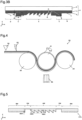
- Fig. 1 is a plan view showing the structure of the display body according to the embodiment.
- Fig. 2 is a cross-sectional view of the display body 2 taken along line a-a in Fig. 1 .
- the display body 2 includes a carrier 3, an embossed layer 4, and a light reflection layer 5.
- the display body 2 further includes various functional layers, such as an adhesive layer used to attach the display body 2 to an article and a protective layer that used to protect the surface of the display body 2.
- the base material of the embossed layer 4 may be a translucent polymer.
- the base material of the embossed layer 4 may also be a thermosetting polymer, a thermoplastic polymer, or a light-cured polymer.
- One of these base materials is used to transfer the uneven structures of a geometric optical structure 6, a wave optical structure 7, and a third structure 8 to the base material from the molds including the uneven structures of the geometric optical structure 6, the wave optical structure 7, and the third structure 8.
- the embossed layer 4 is formed by applying a precursor onto the carrier 3.
- the original plate including a minute structure is pressed against the applied layer and then the precursor is hardened, so that various uneven structures are formed on the surface of the applied layer.
- the original plate including a minute structure is pressed against the layer of the thermoplastic polymer and then the layer of the thermoplastic polymer is softened, so that various uneven structures are formed on the surface of the layer of the thermoplastic polymer.
- the thickness of the embossed layer 4 is set in correspondence with the height of the geometric optical structure 6 and the height of the third structure 8. This allows various uneven structures to be molded at a processing speed that is favorable in productivity and ensures the moldability of the uneven structures.
- the distance between the interface between the embossed layer 4 and the carrier 3 and an approximation surface obtained by approximating, with a flat surface, the uneven surface of the wave optical structure 7 in the wave optical structure region B is the thickness of the embossed layer 4.
- the embossed layer 4 is thick.
- the thickness of the embossed layer 4 is greater than or equal to one times or more height AH of the geometric optical structure 6 and may be approximately twice height AH.
- the embossed layer 4 be thin and the processing speed of the embossed layer 4 be high.
- a smaller cycle of the geometric optical structure 6 tends to be more advantageous for molding.
- a larger cycle of the geometric optical structure 6 tends to be less advantageous. That is, the moldability of the geometric optical structure 6 is ensured more easily when the cycle of the geometric optical structure 6 is smaller, and the moldability of the geometric optical structure 6 is ensured less easily when the cycle of the geometric optical structure 6 is larger.
- the surface of the geometric optical structure 6 may also include a light reflection structure.
- the surface of the geometric optical structure 6 does not include the light reflection structure.
- the light reflection structure may be a reflective metal thin film. Forming the reflective metal thin film on the surface of the uneven structure allows an observer to visually recognize a highly bright reflected light as a display light used to display an image.
- the light reflection structure may be a semi-transmissive thin film.
- a material needs to be used considering of the difference between the refractive index of the semi-transmissive thin film and the refractive index of the embossed layer 4. The use of such a material allows the display body 2 to have the visual effect including at least one of transmission, semi-transmission, and total reflection depending on the angle formed by the angle of an illuminating light and the surface of the uneven structure.
- the third structure 8 may differ from the other structures in hardness.
- the third structure 8 may be lower than the other structures in hardness.
- the hardness of the third structure 8 may decrease in a direction from the carrier 3 toward the light reflection layer 5. Such a structure increases the elasticity of the third structure 8 and is thus likely to prevent the third structure 8 from being destroyed by external force.
- the third structure 8 may be more fluorescent than the geometric optical structure 6 and the wave optical structure 7.
- irradiating the embossed layer 4 with excitation lights allows the light emission of the third structure 8 to become more intense than that of the geometric optical structure 6 and the wave optical structure 7.
- the third structure 8 to produce a latent image.
- the boundary between the geometric optical structure 6 and the third structure 8 and/or the boundary between the wave optical structure 7 and the third structure 8 can be edged. This allows for edging using a boundary where light is emitted by excitation lights.
- the light emitted in the geometric optical structure 6 and the wave optical structure 7 disperses and removes out the light guided to the third structure 8.
- the third structure 8 has a higher fluorescence intensity than the geometric optical structure 6 and the wave optical structure 7.
- the embossed layer 4 may be fluorescent, and width CP of the third structure region C may include multiple values. Furthermore, width CP of the third structure region C may vary continuously in the extending direction of the third structure region C. Such edging through the light emission of the third structure 8 has a dynamic appearance.
- the supplier 24 supplies an uncured precursor that is used to form the embossed layer 4 on the carrier 3.
- the supplier 24 may be a dispenser or a die.
- a precursor layer of the embossed layer 4 is formed on the carrier 3.
- the precursor supplied by the supplier 24 is an ultraviolet-cured composition or an ultraviolet-cured polymer, which have been described above.
- the precursor may be a light-cured composition or a light-cured polymer that is cured by light other than ultraviolet light.
- the heater 25 softens the precursor by heating the precursor that has been supplied by the supplier 24 to the carrier 3. This improves the moldability of the precursor and increases the reactivity of the precursor.
- the plate cylinder 21 includes a body 21a and a mold 21b.
- the body 21a has a columnar shape extending in the extension direction.
- the body 21a may be a roll core.
- the body 21a may include a temperature controller.
- the temperature controller may be a cooler or a heater.
- the mold 21b includes a tubular shape covering the outer circumferential surface of the body 21a.
- the surface of the mold 21b has an uneven shape used to form the geometric optical structure 6 that is transferred to the precursor layer.
- the uneven shape of the mold 21b is transferred to the precursor layer by the pressing roll 22 pressing the precursor layer against the mold 21b.
- the roll-to-roll apparatus 20 may include a back-up roll instead of the plate cylinder 21.
- the mold 21b may be formed using a polymer film.
- the polymer film may have a single-layer structure or a multi-layer structure.
- the thickness of the polymer film may be greater than or equal to 50 ⁇ m and less than or equal to 300 ⁇ m.
- the thickness of the polymer film may be a value measured using a micrometer.
- the head of the micrometer may have a flat tip.
- the diameter of the head of the micrometer may be greater than or equal to 2 mm and less than or equal to 10 mm.
- the formation of the embossed layer 4 including the geometric optical structure 6 allows the display body 2 to record part of a display image that can be formed by the display body 2.
- the heater 25 and the irradiator 26 of the roll-to-roll apparatus 20 may be replaced with a heater that heats a precursor layer in contact with the mold 21b or a precursor layer subsequent to contacting the mold.
- the precursor layer for forming the embossed layer 4 is made of a thermoplastic polymer
- the irradiator 26 simply needs to be omitted from the roll-to-roll apparatus 20 and the heater simply needs to heat the precursor layer to such a degree that the shape of the mold is transferrable on the precursor layer.
- the surface of the mold 21b is an uneven surface.
- the uneven surface includes a geometric optical structure region AM, a wave optical structure region BM, and a third structure region CM.
- the geometric optical structure region AM of the uneven surface is used to form the geometric optical structure 6 of the embossed layer 4.
- the wave optical structure region BM of the uneven surface is used to form the wave optical structure 7 of the embossed layer 4.
- the third structure region CM of the uneven surface is used to form the third structure 8 of the embossed layer 4.
- each of the regions of the uneven surfaces has a shape corresponding to the region of the embossed layer 4 formed by the regions.
- This structure in which the side surface of the third structure 8 is inclined, also allows the original plate to be easily filled with the material of which the embossed layer 4 is made. This ensures the moldability of the third structure 8 and hinders insufficient curing that would result from the oxygen that exists between the original plate and the material of which forming the embossed layer 4 is made. Thus, insufficient peeling of the embossed layer 4 is prevented. Consequently, a fault resulting from insufficient curing in part of the display body 2 is less likely to occur in the display body 2.
- the mold 21b can be formed through electroforming. That is, the mold 21b may be an electroformed mold.
- the electroformed mold can be manufactured by duplicating a master through electroforming plating.
- the electroforming plating causes the shape of the surface of the master to be transferred to the surface of the electroformed mold.
- Examples of the methods for forming the surface of the master include electron beam processing, laser processing, ion beam processing, photolithography, cutting, corroding, and engraving. To form the surface of the mold 21b, any one of these methods may be used to form the surface of the mold 21b on a member that is used to form the mold 21b.
- the mold 21b with a desired surface may be manufactured by manufacturing the surface of the original plate using any one of these methods and then transferring the surface of the original plate to a member that is used to form the mold 21b.
- the mold 21b with a desired surface may be manufactured through electroforming using a master.
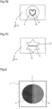
- the wave optical structure region B may be in contact with the third structure region C, and the third structure region C may be in contact with the geometric optical structure region A.
- the third structure region C surrounds the entire wave optical structure region B, and the geometric optical structure region A surrounds the entire third structure region C.
- the wave optical structure region B and the geometric optical structure region A are distanced from each other by the third structure region C. This prevents the occurrence of noise resulting from stray light that occurs between the regions. Accordingly, the visual effect of the display body 2 is expected to improve.
- the geometric optical structure region A, the wave optical structure region B, and the third structure region C form the shape of one circle in the same manner as the example of Fig. 8 .
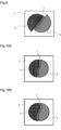
- the third structure region C has a wavy shape in a plan view of the flat surface on which the display body 2 spreads.
- the portion of the geometric optical structure region A in contact with the third structure region C is wavy along the third structure region C.
- the portion of the wave optical structure region B in contact with the third structure region C is wavy along the third structure region C.
- the mold 21b which includes an uneven structure corresponding to the uneven structure of each region is used to transfer, to the surface of the embossed layer 4, the motif (illustration or pattern) formed by combining the above-described three regions.
- the uneven shape of the surface of the mold 21b is formed through electroforming using a matrix as described above.
- the matrix is formed by connecting individually-produced relief patterns with each other and imposing the matrix with the relief patterns.
- the mold 21b used to form the embossed layer 4 has the cross-sectional structure shown in Fig. 11B . That is, the cross-sectional structure of the mold 21b is obtained by reversing the cross-sectional structure of the display body 2.
- the mold 21b is formed through, for example, formation of multiple replicative molds based on the original plate, trimming of the replicative molds, imposition of the replicative molds, formation of plastic molds by replicating the replicative molds, and replication using plating of the plastic molds. In these processes, the mold having a shape of the reversed original plate and the mold having the same shape as the original plate are alternately repeated so that the mold 21b is finally obtained with a desired shape.
- a part of the light reflection layer 5 does not have to be located in the geometric optical structure region A while a part of the light reflection layer 5 is located in the third structure region C and another part of the light reflection layer 5 is located in the wave optical structure region B. That is, the geometric optical structure region A includes only a part of the carrier 3 and a part of the embossed layer 4.
- the wave optical structure region B the reflection achieved by the refraction, absorption, interference, and diffraction of the light by the wave optical structure 7 is obtained as the visual effect of the wave optical structure region B.
- the reflection by the third structure 8 is obtained as the visual effect of the third structure region C.
- the visual effect of the geometric optical structure region A is obtained when transmission in the geometric optical structure region A is observed.
- the geometric optical structure 6 is the above-described microlens
- a dynamic visual effect is achieved during the observation of transmission in the geometric optical structure region A by overlapping the geometric optical structure region A with a printed layer 9 of the microprint and focusing the microlens on the microprint.
- the printed layer 9 of the microprint may include, for example, a character and an illustration.
- the printed layer 9 may be closer to the embossed layer 4 or the light reflection layer 5 on the carrier 3.
- the display body 2 is gained with a visual effect that differs in the observation of reflection and the observation of transmission.
- a part of the light reflection layer 5 does not have to be located in the third structure 8 while a part of the light reflection layer 5 is located in the geometric optical structure region A and another part of the light reflection layer 5 is located in the wave optical structure region B. That is, the third structure region C includes only a part of the carrier 3 and a part of the embossed layer 4.
- the printed layer 9 is observed during the observation of transmission in the third structure region C by overlapping the printed layer 9 with the third structure region C.
- the method for partially forming the light reflection layer i.e., the method for forming the light reflection layer 5 only on a part of the embossed layer 4) will now be described.
- Another method is to, for example, form a mask through mask printing on the portion of the light reflection layer 5 that is to be left on the embossed layer 4 and then corrode, using a corrosive agent, the portion of the light reflection layer 5 on which the mask is not formed, thereby forming the light reflection layer 5 on a part of the light reflection layer 5.
- a water-soluble ink is first printed on the portion of the embossed layer 4 from which the light reflection layer 5 is to be eliminated. Then, after light reflection layer 5 is formed on the entire surface of the embossed layer 4, the water-soluble ink is washed off with water so that a part of the light reflection layer 5 is eliminated.
- the light reflection layer 5 is formed on the entire embossed layer 4.
- vapor deposition or sputtering may be performed.
- a mask layer is formed on the light reflection layer 5 through vapor deposition or sputtering.
- the mask layer may be made of, for example, magnesium fluoride or silica.
- the wave optical structure 7 has a larger surface area than the geometric optical structure 6, and the geometric optical structure 6 has a larger surface area than the third structure 8.
- the portion on the wave optical structure 7 is thinner than the portion on the geometric optical structure 6, and the portion on the geometric optical structure 6 is thinner than the portion on the third structure 8.
- the display body 2 is wet-etching performed for the display body 2 so as to selectively eliminate the thin portions of the light reflection layer 5 (i.e., the portion on the wave optical structure 7 and the portion on the geometric optical structure 6).
- the etchant may be, for example, alkaline NaOH.
- the light reflection layer 5 is formed only on a part of the embossed layer 4 by performing wet-etching of the light reflection layer 5.
- the display body 2 functions as a label when provided with an adhesive layer.
- the label including the display body 2 is attachable to a printed matter or the card 1. That is, the label includes the display body 2 and the adhesive layer and is attached to various articles by the adhesive layer.
- the article to which the label is attached is a labelled article.
- PET may be used for the carrier 3 and an ultraviolet-cured polymer may be used for the embossed layer 4.
- an aluminum layer may be formed on the embossed layer 4 as the light reflection layer 5, and an adhesive layer 10 may be formed on the surface of the embossed layer 4 opposite to the surface that is in contact with the carrier 3.
- the use of the adhesive layer allows the article to support the display body 2.
- the display body 2 is difficult to counterfeit or imitate.
- the label including the display body 2 is supported by the article, the labelled article, which is genuine, is difficult to counterfeit or imitate.
- the display body 2 may have a stripe shape.
- a peel layer is formed between the carrier 3 and the embossed layer 4.
- This provides a transfer foil including the display body 2.
- the display body 2 included in the transfer foil is transferred to a security 11 so as to obtain the security 11 with a label, which is an example of the labelled printed matter.
- the labelled printed matter has an excellent aesthetic appeal.
- the label of the labelled printed matter allows for verification of whether the printed matter is genuine.
- the display body 2 may have the shape of a stripe or a patch.
- a print may be formed on the lower surface and the upper surface of the display body 2.
- the terms "part,” “element,” “pixel,” “cell,” “segment,” “unit,” “display body,” and “article” used in the present disclosure are physical entities. Physical existence can refer to a physical form or a spatial form surrounded by matter.
- the physical entity may be a structure.
- the structure may have a specific function.
- the combination of structures having a specific function can provide a synergistic effect because of the combination of each function of each structure.
Landscapes
- Manufacturing & Machinery (AREA)
- Engineering & Computer Science (AREA)
- Physics & Mathematics (AREA)
- Optics & Photonics (AREA)
- Toxicology (AREA)
- Health & Medical Sciences (AREA)
- Electromagnetism (AREA)
- General Health & Medical Sciences (AREA)
- General Physics & Mathematics (AREA)
- Chemical & Material Sciences (AREA)
- Chemical Kinetics & Catalysis (AREA)
- General Chemical & Material Sciences (AREA)
- Diffracting Gratings Or Hologram Optical Elements (AREA)
- Shaping Of Tube Ends By Bending Or Straightening (AREA)
- Infusion, Injection, And Reservoir Apparatuses (AREA)
- Credit Cards Or The Like (AREA)
- Optical Elements Other Than Lenses (AREA)
Claims (7)
- Corps d'affichage (2), comprenant une couche gaufrée (4), dans lequella couche gaufrée (4) comporte une région de structure optique géométrique (A), et une région de structure optique ondulée (B),la couche gaufrée (4) comporte une première structure irrégulière (6) dans la région de structure optique géométrique (A), la première structure irrégulière (6) ayant une hauteur (AH) supérieure ou égale à 0,5 µm et inférieure à 30 µm, etla couche gaufrée (4) comporte une deuxième structure irrégulière (7) dans la région de structure optique ondulée (B),la deuxième structure irrégulière (7) ayant une hauteur (BH) supérieure ou égale à 100 nm et inférieure à 500 nm,la couche gaufrée (4) comporte une troisième région de structure (C), la troisième région de structure (C) étant située entre la région de structure optique géométrique (A) et la région de structure optique ondulée (B),la couche gaufrée (4) comporte une troisième structure irrégulière (8) dans la troisième région de structure (C), la troisième structure irrégulière (8) ayant une hauteur (CH) supérieure ou égale à la moitié de l'épaisseur de la couche gaufrée (4) et inférieure ou égale à deux fois la hauteur (AH) de la première structure irrégulière, la hauteur (CH) de la troisième structure irrégulière (8) étant supérieure à la hauteur (AH) de la première structure irrégulière (6), etle corps d'affichage (2) comprend en outre une couche réfléchissant la lumière (5), la couche réfléchissant la lumière (5) étant une couche métallique,la couche réfléchissant la lumière (5) recouvre la région de structure optique géométrique (A), la région de structure optique ondulée (B) et la troisième région de structure (C), ou la couche réfléchissant la lumière (5) recouvre l'une des régions de structure optique géométrique (A) et de structure optique ondulée (B) et recouvre la troisième région de structure (C), ou la couche réfléchissant la lumière (5) recouvre la région de structure optique géométrique (A) et la région de structure optique ondulée (B) et ne recouvre pas la troisième région de structure (C).
- Corps d'affichage (2) selon la revendication 1, dans lequel la troisième région de structure (C) est en contact avec la région de structure optique géométrique (A) et la région de structure optique ondulée (B).
- Corps d'affichage (2) selon la revendication 1, dans lequel la troisième région de structure (C) est en contact avec l'une des régions de structure optique géométrique (A) et de structure optique ondulée (B).
- Corps d'affichage (2) selon l'une quelconque des revendications 1 à 3, dans lequella troisième région de structure (C) a une largeur supérieure ou égale à la hauteur (CH) de la troisième structure irrégulière (8) et inférieure ou égale à 500 µm, etla largeur de la troisième région de structure (C) est une distance entre des bords de la troisième région de structure (C) dans une direction dans laquelle la région de structure optique géométrique (A) fait face à la région de structure optique ondulée (B).
- Corps d'affichage (2) selon l'une quelconque des revendications 1 à 4, dans lequelune partie où une surface supérieure et une surface latérale qui définissent une forme extérieure de la troisième structure irrégulière (8) se croisent dans une section transversale qui est orthogonale à une surface plane sur laquelle la couche gaufrée (4) s'étend est un coin de la troisième structure (8), etle coin de la troisième structure irrégulière (8) est arrondi.
- Corps d'affichage (2) selon la revendication 5, comprenant en outre un support (3) qui soutient la couche gaufrée (4), dans lequel
la surface latérale de la troisième structure irrégulière (8) est inclinée par rapport au support (3). - Imprimé étiqueté, comprenant :une étiquette comportantle corps d'affichage (2) selon l'une quelconque des revendications 1 à 6, etune couche adhésive (10) ; etun imprimé (11),dans lequel l'étiquette est fixée à l'imprimé (11) par la couche adhésive (10).
Applications Claiming Priority (4)
| Application Number | Priority Date | Filing Date | Title |
|---|---|---|---|
| JP2019000561 | 2019-01-07 | ||
| JP2019048095 | 2019-03-15 | ||
| PCT/JP2020/000156 WO2020145265A1 (fr) | 2019-01-07 | 2020-01-07 | Corps d'indicateur et matière imprimée étiqueté |
| EP20738217.7A EP3910384B1 (fr) | 2019-01-07 | 2020-01-07 | Corps d'indicateur et matière imprimée étiqueté |
Related Parent Applications (2)
| Application Number | Title | Priority Date | Filing Date |
|---|---|---|---|
| EP20738217.7A Division-Into EP3910384B1 (fr) | 2019-01-07 | 2020-01-07 | Corps d'indicateur et matière imprimée étiqueté |
| EP20738217.7A Division EP3910384B1 (fr) | 2019-01-07 | 2020-01-07 | Corps d'indicateur et matière imprimée étiqueté |
Publications (3)
| Publication Number | Publication Date |
|---|---|
| EP4249281A2 EP4249281A2 (fr) | 2023-09-27 |
| EP4249281A3 EP4249281A3 (fr) | 2024-01-03 |
| EP4249281B1 true EP4249281B1 (fr) | 2025-04-16 |
Family
ID=71521645
Family Applications (3)
| Application Number | Title | Priority Date | Filing Date |
|---|---|---|---|
| EP23189982.4A Active EP4249281B1 (fr) | 2019-01-07 | 2020-01-07 | Corps d'indicateur et matière imprimée étiquetée |
| EP20738217.7A Active EP3910384B1 (fr) | 2019-01-07 | 2020-01-07 | Corps d'indicateur et matière imprimée étiqueté |
| EP23189981.6A Active EP4249280B1 (fr) | 2019-01-07 | 2020-01-07 | Corps d'indicateur et matière imprimée étiquetée |
Family Applications After (2)
| Application Number | Title | Priority Date | Filing Date |
|---|---|---|---|
| EP20738217.7A Active EP3910384B1 (fr) | 2019-01-07 | 2020-01-07 | Corps d'indicateur et matière imprimée étiqueté |
| EP23189981.6A Active EP4249280B1 (fr) | 2019-01-07 | 2020-01-07 | Corps d'indicateur et matière imprimée étiquetée |
Country Status (4)
| Country | Link |
|---|---|
| EP (3) | EP4249281B1 (fr) |
| JP (1) | JP7318666B2 (fr) |
| AU (1) | AU2020205517B2 (fr) |
| WO (1) | WO2020145265A1 (fr) |
Families Citing this family (3)
| Publication number | Priority date | Publication date | Assignee | Title |
|---|---|---|---|---|
| EP4607253A3 (fr) * | 2018-07-05 | 2025-11-26 | Toppan Printing Co., Ltd. | Structure optique |
| JP7318666B2 (ja) | 2019-01-07 | 2023-08-01 | 凸版印刷株式会社 | 表示体、および、ラベル付き印刷物 |
| JP2023148806A (ja) * | 2022-03-30 | 2023-10-13 | パナソニックIpマネジメント株式会社 | 高さが異なる微細パターンを有する原盤及びインプリント素子 |
Citations (14)
| Publication number | Priority date | Publication date | Assignee | Title |
|---|---|---|---|---|
| EP0401466A1 (fr) | 1989-06-05 | 1990-12-12 | Landis & Gyr Technology Innovation AG | Stratifié avec des structures à diffraction |
| US5538753A (en) | 1991-10-14 | 1996-07-23 | Landis & Gyr Betriebs Ag | Security element |
| EP1599345B1 (fr) | 2003-02-26 | 2007-08-29 | Giesecke & Devrient GmbH | Element de securite |
| DE102006037431A1 (de) | 2006-08-09 | 2008-04-17 | Ovd Kinegram Ag | Verfahren zur Herstellung eines Mehrschichtkörpers sowie Mehrschichtkörper |
| EP2077459A1 (fr) | 2006-10-24 | 2009-07-08 | Toppan Printing Co., Ltd. | Corps d'affichage et article etiquete |
| DE102008008685A1 (de) | 2008-02-12 | 2009-08-13 | Giesecke & Devrient Gmbh | Sicherheitselement und Verfahren zu seiner Herstellung |
| EP2264488A1 (fr) | 2008-04-18 | 2010-12-22 | Toppan Printing Co., Ltd. | Matériau d'étiquetage et article de marchandise étiqueté |
| EP1747100B1 (fr) | 2004-04-03 | 2011-03-16 | OVD Kinegram AG | Element de securite se presentant sous la forme d'un corps en pellicule multicouche |
| EP2508922A1 (fr) | 2009-12-01 | 2012-10-10 | Toppan Printing Co., Ltd. | Corps de présentation et article étiqueté |
| DE102011107154A1 (de) | 2011-07-14 | 2013-01-17 | Giesecke & Devrient Gmbh | Optisch variables Element, insbesondere Sicherheitselement für einen Datenträger |
| JP5272438B2 (ja) | 2008-02-19 | 2013-08-28 | 凸版印刷株式会社 | 表示体及びラベル付き物品 |
| JP2016114776A (ja) | 2014-12-15 | 2016-06-23 | 凸版印刷株式会社 | 偽造防止積層体及びその製造方法 |
| EP3208099A1 (fr) | 2014-10-16 | 2017-08-23 | Zhongchao Special Security Technology Co., Ltd | Élément anti-contrefaçon optique et produit anti-contrefaçon optique |
| DE102017003281A1 (de) | 2017-04-04 | 2018-10-04 | Giesecke+Devrient Currency Technology Gmbh | Sicherheitselement mit Reliefstruktur und Herstellungsverfahren hierfür |
Family Cites Families (17)
| Publication number | Priority date | Publication date | Assignee | Title |
|---|---|---|---|---|
| US5058992A (en) | 1988-09-07 | 1991-10-22 | Toppan Printing Co., Ltd. | Method for producing a display with a diffraction grating pattern and a display produced by the method |
| DE102007039996B4 (de) | 2007-02-07 | 2020-09-24 | Leonhard Kurz Stiftung & Co. Kg | Sicherheitselement für ein Sicherheitsdokument und Verfahren zu seiner Herstellung |
| JP5169093B2 (ja) * | 2007-09-12 | 2013-03-27 | 凸版印刷株式会社 | 偽造防止積層体、偽造防止転写箔、偽造防止シール、偽造防止媒体、及びこれらの製造方法 |
| JP5266770B2 (ja) | 2008-01-22 | 2013-08-21 | 凸版印刷株式会社 | レリーフ構造形成層からなる表示体及びラベル付き物品 |
| DE102011114644A1 (de) | 2011-09-30 | 2013-04-04 | Giesecke & Devrient Gmbh | Sicherheitselement mit mehreren optisch variablen Strukturen und einem kinematischen Effekt |
| GB201301788D0 (en) | 2013-02-01 | 2013-03-20 | Rue De Int Ltd | Security devices and methods of manufacture thereof |
| GB2514337B (en) | 2013-05-17 | 2020-01-15 | De La Rue Int Ltd | Security documents and methods of manufacture thereof |
| DE102013105246B4 (de) | 2013-05-22 | 2017-03-23 | Leonhard Kurz Stiftung & Co. Kg | Optisch variables Element |
| DE102013108666A1 (de) | 2013-08-09 | 2015-03-05 | Leonhard Kurz Stiftung & Co. Kg | Verfahren zur Herstellung eines Mehrschichtkörpers sowie Mehrschichtkörper |
| GB201400910D0 (en) | 2014-01-20 | 2014-03-05 | Rue De Int Ltd | Security elements and methods of their manufacture |
| CN105015216B (zh) | 2014-04-29 | 2017-06-16 | 中钞特种防伪科技有限公司 | 一种光学防伪元件及制备光学防伪元件的方法 |
| DE112015005090T5 (de) | 2014-11-10 | 2017-08-03 | Toppan Printing Co., Ltd. | Optisches Element zur Fälschungssicherung |
| JP2016114917A (ja) | 2014-12-18 | 2016-06-23 | 凸版印刷株式会社 | 表示体 |
| FR3031697B1 (fr) | 2015-01-16 | 2020-12-18 | Hologram Ind | Composant optique de securite. |
| CN108603955B (zh) | 2016-02-09 | 2021-09-14 | 凸版印刷株式会社 | 防伪用光学元件以及信息记录介质 |
| DE102016002451A1 (de) | 2016-02-29 | 2017-08-31 | Giesecke & Devrient Gmbh | Prägeplatte, Herstellungsverfahren und geprägtes Sicherheitselement |
| JP7318666B2 (ja) | 2019-01-07 | 2023-08-01 | 凸版印刷株式会社 | 表示体、および、ラベル付き印刷物 |
-
2020
- 2020-01-07 JP JP2020565155A patent/JP7318666B2/ja active Active
- 2020-01-07 WO PCT/JP2020/000156 patent/WO2020145265A1/fr not_active Ceased
- 2020-01-07 EP EP23189982.4A patent/EP4249281B1/fr active Active
- 2020-01-07 EP EP20738217.7A patent/EP3910384B1/fr active Active
- 2020-01-07 AU AU2020205517A patent/AU2020205517B2/en active Active
- 2020-01-07 EP EP23189981.6A patent/EP4249280B1/fr active Active
Patent Citations (15)
| Publication number | Priority date | Publication date | Assignee | Title |
|---|---|---|---|---|
| EP0401466A1 (fr) | 1989-06-05 | 1990-12-12 | Landis & Gyr Technology Innovation AG | Stratifié avec des structures à diffraction |
| US5538753A (en) | 1991-10-14 | 1996-07-23 | Landis & Gyr Betriebs Ag | Security element |
| EP1599345B1 (fr) | 2003-02-26 | 2007-08-29 | Giesecke & Devrient GmbH | Element de securite |
| EP1747100B1 (fr) | 2004-04-03 | 2011-03-16 | OVD Kinegram AG | Element de securite se presentant sous la forme d'un corps en pellicule multicouche |
| EP2049345B1 (fr) | 2006-08-09 | 2013-06-19 | OVD Kinegram AG | Procédé de fabrication d'un corps multicouche et corps multicouche |
| DE102006037431A1 (de) | 2006-08-09 | 2008-04-17 | Ovd Kinegram Ag | Verfahren zur Herstellung eines Mehrschichtkörpers sowie Mehrschichtkörper |
| EP2077459A1 (fr) | 2006-10-24 | 2009-07-08 | Toppan Printing Co., Ltd. | Corps d'affichage et article etiquete |
| DE102008008685A1 (de) | 2008-02-12 | 2009-08-13 | Giesecke & Devrient Gmbh | Sicherheitselement und Verfahren zu seiner Herstellung |
| JP5272438B2 (ja) | 2008-02-19 | 2013-08-28 | 凸版印刷株式会社 | 表示体及びラベル付き物品 |
| EP2264488A1 (fr) | 2008-04-18 | 2010-12-22 | Toppan Printing Co., Ltd. | Matériau d'étiquetage et article de marchandise étiqueté |
| EP2508922A1 (fr) | 2009-12-01 | 2012-10-10 | Toppan Printing Co., Ltd. | Corps de présentation et article étiqueté |
| DE102011107154A1 (de) | 2011-07-14 | 2013-01-17 | Giesecke & Devrient Gmbh | Optisch variables Element, insbesondere Sicherheitselement für einen Datenträger |
| EP3208099A1 (fr) | 2014-10-16 | 2017-08-23 | Zhongchao Special Security Technology Co., Ltd | Élément anti-contrefaçon optique et produit anti-contrefaçon optique |
| JP2016114776A (ja) | 2014-12-15 | 2016-06-23 | 凸版印刷株式会社 | 偽造防止積層体及びその製造方法 |
| DE102017003281A1 (de) | 2017-04-04 | 2018-10-04 | Giesecke+Devrient Currency Technology Gmbh | Sicherheitselement mit Reliefstruktur und Herstellungsverfahren hierfür |
Non-Patent Citations (5)
| Title |
|---|
| ANONYMOUS: "The commemorative Ninety Crown Note is finally on sale ", STATNI TISKARNA CENIN, S.P., XP093194613, Retrieved from the Internet <URL:https://stc.cz/en/the-commemorative-ninety-crown-note-is-finally-on-sale/> |
| D13 - Broschüre ohne eingelegte Musterbanknote |
| D14 - Broschüre mit eingelegter Musterbanknote |
| D16 - Eidesstattliche Versicherung |
| D17 - Untersuchungsbericht |
Also Published As
| Publication number | Publication date |
|---|---|
| AU2020205517B2 (en) | 2025-01-23 |
| EP4249280A2 (fr) | 2023-09-27 |
| EP3910384B1 (fr) | 2023-09-20 |
| WO2020145265A1 (fr) | 2020-07-16 |
| EP4249281A2 (fr) | 2023-09-27 |
| JP7318666B2 (ja) | 2023-08-01 |
| JPWO2020145265A1 (ja) | 2021-11-18 |
| EP4249280A3 (fr) | 2024-01-03 |
| AU2020205517A1 (en) | 2021-08-26 |
| EP4249280B1 (fr) | 2025-04-23 |
| EP4249281A3 (fr) | 2024-01-03 |
| EP3910384A1 (fr) | 2021-11-17 |
| EP3910384A4 (fr) | 2022-11-16 |
Similar Documents
| Publication | Publication Date | Title |
|---|---|---|
| US10112432B2 (en) | Security device | |
| JP5741125B2 (ja) | 表示体及びラベル付き物品 | |
| EP4249281B1 (fr) | Corps d'indicateur et matière imprimée étiquetée | |
| GB2552083A (en) | Methods of manufacturing security documents and security devices | |
| JP6201289B2 (ja) | 画像表示体及び情報媒体 | |
| JPH0948171A (ja) | 部分的に透明な機密保護要素を製造する方法 | |
| JPWO2017068769A1 (ja) | 表示体、および表示体付き物品、ならびに表示体の観察方法 | |
| JP3969592B2 (ja) | 対象物の識別媒体 | |
| JP4391102B2 (ja) | 真偽判定体 | |
| JP5504732B2 (ja) | 表示体及びラベル付き物品 | |
| JP5245430B2 (ja) | 表示体及びラベル付き物品 | |
| JP2014240892A (ja) | 光学素子及び光学素子を形成するための転写箔の製造方法 | |
| KR20160125706A (ko) | 극소형 이미지 패턴을 가지는 렌즈시트 및 그 제조방법 | |
| EP3819684B1 (fr) | Structure optique | |
| CN116867649A (zh) | 制造具有微成像元件的防伪元件的方法 | |
| JP2007003673A (ja) | 偽造防止媒体とそれに使用する偽造防止体及び偽造防止体転写箔 | |
| JP5604860B2 (ja) | 偽造防止用紙 | |
| JP2005035115A (ja) | 真偽判定体 | |
| EP2081058A2 (fr) | Structure de barrière avec relief à sa surface | |
| JP7326833B2 (ja) | 発色構造体、表示体、及び、発色構造体の製造方法 | |
| JP2003285527A (ja) | 光反射性基材を有する積層体 | |
| JP2016212439A (ja) | 表示体及びラベル付き物品 | |
| JP5994899B2 (ja) | 表示体及びラベル付き物品 | |
| WO2017159636A1 (fr) | Corps formant structure de diffraction, article doté d'un corps formant structure de diffraction et procédé de production d'un corps formant structure de diffraction |
Legal Events
| Date | Code | Title | Description |
|---|---|---|---|
| PUAI | Public reference made under article 153(3) epc to a published international application that has entered the european phase |
Free format text: ORIGINAL CODE: 0009012 |
|
| STAA | Information on the status of an ep patent application or granted ep patent |
Free format text: STATUS: REQUEST FOR EXAMINATION WAS MADE |
|
| 17P | Request for examination filed |
Effective date: 20230807 |
|
| AC | Divisional application: reference to earlier application |
Ref document number: 3910384 Country of ref document: EP Kind code of ref document: P |
|
| AK | Designated contracting states |
Kind code of ref document: A2 Designated state(s): AL AT BE BG CH CY CZ DE DK EE ES FI FR GB GR HR HU IE IS IT LI LT LU LV MC MK MT NL NO PL PT RO RS SE SI SK SM TR |
|
| REG | Reference to a national code |
Ref legal event code: R079 Free format text: PREVIOUS MAIN CLASS: B42D0025328000 Ipc: G02B0003000000 Ref country code: DE Ref legal event code: R079 Ref document number: 602020049781 Country of ref document: DE Free format text: PREVIOUS MAIN CLASS: B42D0025328000 Ipc: G02B0003000000 |
|
| PUAL | Search report despatched |
Free format text: ORIGINAL CODE: 0009013 |
|
| AK | Designated contracting states |
Kind code of ref document: A3 Designated state(s): AL AT BE BG CH CY CZ DE DK EE ES FI FR GB GR HR HU IE IS IT LI LT LU LV MC MK MT NL NO PL PT RO RS SE SI SK SM TR |
|
| RIC1 | Information provided on ipc code assigned before grant |
Ipc: B42D 25/328 20140101ALI20231127BHEP Ipc: G02B 5/18 20060101ALI20231127BHEP Ipc: G02B 5/04 20060101ALI20231127BHEP Ipc: G02B 5/00 20060101ALI20231127BHEP Ipc: G09F 3/02 20060101ALI20231127BHEP Ipc: G02B 3/00 20060101AFI20231127BHEP |
|
| GRAP | Despatch of communication of intention to grant a patent |
Free format text: ORIGINAL CODE: EPIDOSNIGR1 |
|
| STAA | Information on the status of an ep patent application or granted ep patent |
Free format text: STATUS: GRANT OF PATENT IS INTENDED |
|
| INTG | Intention to grant announced |
Effective date: 20241115 |
|
| GRAS | Grant fee paid |
Free format text: ORIGINAL CODE: EPIDOSNIGR3 |
|
| GRAA | (expected) grant |
Free format text: ORIGINAL CODE: 0009210 |
|
| STAA | Information on the status of an ep patent application or granted ep patent |
Free format text: STATUS: THE PATENT HAS BEEN GRANTED |
|
| AC | Divisional application: reference to earlier application |
Ref document number: 3910384 Country of ref document: EP Kind code of ref document: P |
|
| AK | Designated contracting states |
Kind code of ref document: B1 Designated state(s): AL AT BE BG CH CY CZ DE DK EE ES FI FR GB GR HR HU IE IS IT LI LT LU LV MC MK MT NL NO PL PT RO RS SE SI SK SM TR |
|
| REG | Reference to a national code |
Ref country code: GB Ref legal event code: FG4D |
|
| REG | Reference to a national code |
Ref country code: CH Ref legal event code: EP |
|
| REG | Reference to a national code |
Ref country code: IE Ref legal event code: FG4D |
|
| REG | Reference to a national code |
Ref country code: DE Ref legal event code: R096 Ref document number: 602020049781 Country of ref document: DE |
|
| REG | Reference to a national code |
Ref country code: NL Ref legal event code: MP Effective date: 20250416 |
|
| PG25 | Lapsed in a contracting state [announced via postgrant information from national office to epo] |
Ref country code: NL Free format text: LAPSE BECAUSE OF FAILURE TO SUBMIT A TRANSLATION OF THE DESCRIPTION OR TO PAY THE FEE WITHIN THE PRESCRIBED TIME-LIMIT Effective date: 20250416 |
|
| PG25 | Lapsed in a contracting state [announced via postgrant information from national office to epo] |
Ref country code: FI Free format text: LAPSE BECAUSE OF FAILURE TO SUBMIT A TRANSLATION OF THE DESCRIPTION OR TO PAY THE FEE WITHIN THE PRESCRIBED TIME-LIMIT Effective date: 20250416 Ref country code: PT Free format text: LAPSE BECAUSE OF FAILURE TO SUBMIT A TRANSLATION OF THE DESCRIPTION OR TO PAY THE FEE WITHIN THE PRESCRIBED TIME-LIMIT Effective date: 20250818 Ref country code: ES Free format text: LAPSE BECAUSE OF FAILURE TO SUBMIT A TRANSLATION OF THE DESCRIPTION OR TO PAY THE FEE WITHIN THE PRESCRIBED TIME-LIMIT Effective date: 20250416 |
|
| REG | Reference to a national code |
Ref country code: LT Ref legal event code: MG9D |
|
| PG25 | Lapsed in a contracting state [announced via postgrant information from national office to epo] |
Ref country code: NO Free format text: LAPSE BECAUSE OF FAILURE TO SUBMIT A TRANSLATION OF THE DESCRIPTION OR TO PAY THE FEE WITHIN THE PRESCRIBED TIME-LIMIT Effective date: 20250716 Ref country code: GR Free format text: LAPSE BECAUSE OF FAILURE TO SUBMIT A TRANSLATION OF THE DESCRIPTION OR TO PAY THE FEE WITHIN THE PRESCRIBED TIME-LIMIT Effective date: 20250717 |
|
| PG25 | Lapsed in a contracting state [announced via postgrant information from national office to epo] |
Ref country code: PL Free format text: LAPSE BECAUSE OF FAILURE TO SUBMIT A TRANSLATION OF THE DESCRIPTION OR TO PAY THE FEE WITHIN THE PRESCRIBED TIME-LIMIT Effective date: 20250416 |
|
| PG25 | Lapsed in a contracting state [announced via postgrant information from national office to epo] |
Ref country code: BG Free format text: LAPSE BECAUSE OF FAILURE TO SUBMIT A TRANSLATION OF THE DESCRIPTION OR TO PAY THE FEE WITHIN THE PRESCRIBED TIME-LIMIT Effective date: 20250416 |
|
| PG25 | Lapsed in a contracting state [announced via postgrant information from national office to epo] |
Ref country code: HR Free format text: LAPSE BECAUSE OF FAILURE TO SUBMIT A TRANSLATION OF THE DESCRIPTION OR TO PAY THE FEE WITHIN THE PRESCRIBED TIME-LIMIT Effective date: 20250416 |
|
| PG25 | Lapsed in a contracting state [announced via postgrant information from national office to epo] |
Ref country code: RS Free format text: LAPSE BECAUSE OF FAILURE TO SUBMIT A TRANSLATION OF THE DESCRIPTION OR TO PAY THE FEE WITHIN THE PRESCRIBED TIME-LIMIT Effective date: 20250716 |
|
| PG25 | Lapsed in a contracting state [announced via postgrant information from national office to epo] |
Ref country code: IS Free format text: LAPSE BECAUSE OF FAILURE TO SUBMIT A TRANSLATION OF THE DESCRIPTION OR TO PAY THE FEE WITHIN THE PRESCRIBED TIME-LIMIT Effective date: 20250816 |
|
| PG25 | Lapsed in a contracting state [announced via postgrant information from national office to epo] |
Ref country code: LV Free format text: LAPSE BECAUSE OF FAILURE TO SUBMIT A TRANSLATION OF THE DESCRIPTION OR TO PAY THE FEE WITHIN THE PRESCRIBED TIME-LIMIT Effective date: 20250416 |
|
| REG | Reference to a national code |
Ref country code: DE Ref legal event code: R026 Ref document number: 602020049781 Country of ref document: DE |
|
| PG25 | Lapsed in a contracting state [announced via postgrant information from national office to epo] |
Ref country code: DK Free format text: LAPSE BECAUSE OF FAILURE TO SUBMIT A TRANSLATION OF THE DESCRIPTION OR TO PAY THE FEE WITHIN THE PRESCRIBED TIME-LIMIT Effective date: 20250416 Ref country code: SM Free format text: LAPSE BECAUSE OF FAILURE TO SUBMIT A TRANSLATION OF THE DESCRIPTION OR TO PAY THE FEE WITHIN THE PRESCRIBED TIME-LIMIT Effective date: 20250416 |
|
| PLBI | Opposition filed |
Free format text: ORIGINAL CODE: 0009260 |
|
| PGFP | Annual fee paid to national office [announced via postgrant information from national office to epo] |
Ref country code: CZ Payment date: 20251219 Year of fee payment: 7 |
|
| REG | Reference to a national code |
Ref country code: CH Ref legal event code: L11 Free format text: ST27 STATUS EVENT CODE: U-0-0-L10-L11 (AS PROVIDED BY THE NATIONAL OFFICE) Effective date: 20260121 |
|
| PLAB | Opposition data, opponent's data or that of the opponent's representative modified |
Free format text: ORIGINAL CODE: 0009299OPPO |
|
| PLBI | Opposition filed |
Free format text: ORIGINAL CODE: 0009260 |
|
| PG25 | Lapsed in a contracting state [announced via postgrant information from national office to epo] |
Ref country code: EE Free format text: LAPSE BECAUSE OF FAILURE TO SUBMIT A TRANSLATION OF THE DESCRIPTION OR TO PAY THE FEE WITHIN THE PRESCRIBED TIME-LIMIT Effective date: 20250416 |
|
| PG25 | Lapsed in a contracting state [announced via postgrant information from national office to epo] |
Ref country code: SK Free format text: LAPSE BECAUSE OF FAILURE TO SUBMIT A TRANSLATION OF THE DESCRIPTION OR TO PAY THE FEE WITHIN THE PRESCRIBED TIME-LIMIT Effective date: 20250416 |
|
| PG25 | Lapsed in a contracting state [announced via postgrant information from national office to epo] |
Ref country code: IT Free format text: LAPSE BECAUSE OF FAILURE TO SUBMIT A TRANSLATION OF THE DESCRIPTION OR TO PAY THE FEE WITHIN THE PRESCRIBED TIME-LIMIT Effective date: 20250416 |
|
| REG | Reference to a national code |
Ref country code: CH Ref legal event code: L10 Free format text: ST27 STATUS EVENT CODE: U-0-0-L10-L00 (AS PROVIDED BY THE NATIONAL OFFICE) Effective date: 20260128 |
|
| PLAX | Notice of opposition and request to file observation + time limit sent |
Free format text: ORIGINAL CODE: EPIDOSNOBS2 |
|
| 26 | Opposition filed |
Opponent name: HUECK FOLIEN GMBH Effective date: 20260109 |
|
| 26 | Opposition filed |
Opponent name: GIESECKE+DEVRIENT MOBILE SECURITY GMBH Effective date: 20260116 |
|
| R26 | Opposition filed (corrected) |
Opponent name: HUECK FOLIEN GMBH Effective date: 20260109 |
|
| PGFP | Annual fee paid to national office [announced via postgrant information from national office to epo] |
Ref country code: DE Payment date: 20251203 Year of fee payment: 7 |
|
| PGFP | Annual fee paid to national office [announced via postgrant information from national office to epo] |
Ref country code: AT Payment date: 20251230 Year of fee payment: 7 |