EP4249631A1 - Verfahren zur herstellung einer dünnschicht - Google Patents
Verfahren zur herstellung einer dünnschicht Download PDFInfo
- Publication number
- EP4249631A1 EP4249631A1 EP21894642.4A EP21894642A EP4249631A1 EP 4249631 A1 EP4249631 A1 EP 4249631A1 EP 21894642 A EP21894642 A EP 21894642A EP 4249631 A1 EP4249631 A1 EP 4249631A1
- Authority
- EP
- European Patent Office
- Prior art keywords
- thin
- film
- raw material
- zirconium
- substrate
- Prior art date
- Legal status (The legal status is an assumption and is not a legal conclusion. Google has not performed a legal analysis and makes no representation as to the accuracy of the status listed.)
- Pending
Links
Images

Classifications
-
- C—CHEMISTRY; METALLURGY
- C23—COATING METALLIC MATERIAL; COATING MATERIAL WITH METALLIC MATERIAL; CHEMICAL SURFACE TREATMENT; DIFFUSION TREATMENT OF METALLIC MATERIAL; COATING BY VACUUM EVAPORATION, BY SPUTTERING, BY ION IMPLANTATION OR BY CHEMICAL VAPOUR DEPOSITION, IN GENERAL; INHIBITING CORROSION OF METALLIC MATERIAL OR INCRUSTATION IN GENERAL
- C23C—COATING METALLIC MATERIAL; COATING MATERIAL WITH METALLIC MATERIAL; SURFACE TREATMENT OF METALLIC MATERIAL BY DIFFUSION INTO THE SURFACE, BY CHEMICAL CONVERSION OR SUBSTITUTION; COATING BY VACUUM EVAPORATION, BY SPUTTERING, BY ION IMPLANTATION OR BY CHEMICAL VAPOUR DEPOSITION, IN GENERAL
- C23C16/00—Chemical coating by decomposition of gaseous compounds, without leaving reaction products of surface material in the coating, i.e. chemical vapour deposition [CVD] processes
- C23C16/22—Chemical coating by decomposition of gaseous compounds, without leaving reaction products of surface material in the coating, i.e. chemical vapour deposition [CVD] processes characterised by the deposition of inorganic material, other than metallic material
- C23C16/30—Deposition of compounds, mixtures or solid solutions, e.g. borides, carbides, nitrides
- C23C16/40—Oxides
-
- C—CHEMISTRY; METALLURGY
- C23—COATING METALLIC MATERIAL; COATING MATERIAL WITH METALLIC MATERIAL; CHEMICAL SURFACE TREATMENT; DIFFUSION TREATMENT OF METALLIC MATERIAL; COATING BY VACUUM EVAPORATION, BY SPUTTERING, BY ION IMPLANTATION OR BY CHEMICAL VAPOUR DEPOSITION, IN GENERAL; INHIBITING CORROSION OF METALLIC MATERIAL OR INCRUSTATION IN GENERAL
- C23C—COATING METALLIC MATERIAL; COATING MATERIAL WITH METALLIC MATERIAL; SURFACE TREATMENT OF METALLIC MATERIAL BY DIFFUSION INTO THE SURFACE, BY CHEMICAL CONVERSION OR SUBSTITUTION; COATING BY VACUUM EVAPORATION, BY SPUTTERING, BY ION IMPLANTATION OR BY CHEMICAL VAPOUR DEPOSITION, IN GENERAL
- C23C16/00—Chemical coating by decomposition of gaseous compounds, without leaving reaction products of surface material in the coating, i.e. chemical vapour deposition [CVD] processes
- C23C16/22—Chemical coating by decomposition of gaseous compounds, without leaving reaction products of surface material in the coating, i.e. chemical vapour deposition [CVD] processes characterised by the deposition of inorganic material, other than metallic material
- C23C16/30—Deposition of compounds, mixtures or solid solutions, e.g. borides, carbides, nitrides
- C23C16/40—Oxides
- C23C16/405—Oxides of refractory metals or yttrium
-
- H—ELECTRICITY
- H10—SEMICONDUCTOR DEVICES; ELECTRIC SOLID-STATE DEVICES NOT OTHERWISE PROVIDED FOR
- H10P—GENERIC PROCESSES OR APPARATUS FOR THE MANUFACTURE OR TREATMENT OF DEVICES COVERED BY CLASS H10
- H10P14/00—Formation of materials, e.g. in the shape of layers or pillars
- H10P14/60—Formation of materials, e.g. in the shape of layers or pillars of insulating materials
- H10P14/63—Formation of materials, e.g. in the shape of layers or pillars of insulating materials characterised by the formation processes
- H10P14/6326—Deposition processes
- H10P14/6328—Deposition from the gas or vapour phase
- H10P14/6334—Deposition from the gas or vapour phase using decomposition or reaction of gaseous or vapour phase compounds, i.e. chemical vapour deposition
- H10P14/6339—Deposition from the gas or vapour phase using decomposition or reaction of gaseous or vapour phase compounds, i.e. chemical vapour deposition deposition by cyclic CVD, e.g. ALD, ALE or pulsed CVD
-
- C—CHEMISTRY; METALLURGY
- C23—COATING METALLIC MATERIAL; COATING MATERIAL WITH METALLIC MATERIAL; CHEMICAL SURFACE TREATMENT; DIFFUSION TREATMENT OF METALLIC MATERIAL; COATING BY VACUUM EVAPORATION, BY SPUTTERING, BY ION IMPLANTATION OR BY CHEMICAL VAPOUR DEPOSITION, IN GENERAL; INHIBITING CORROSION OF METALLIC MATERIAL OR INCRUSTATION IN GENERAL
- C23C—COATING METALLIC MATERIAL; COATING MATERIAL WITH METALLIC MATERIAL; SURFACE TREATMENT OF METALLIC MATERIAL BY DIFFUSION INTO THE SURFACE, BY CHEMICAL CONVERSION OR SUBSTITUTION; COATING BY VACUUM EVAPORATION, BY SPUTTERING, BY ION IMPLANTATION OR BY CHEMICAL VAPOUR DEPOSITION, IN GENERAL
- C23C16/00—Chemical coating by decomposition of gaseous compounds, without leaving reaction products of surface material in the coating, i.e. chemical vapour deposition [CVD] processes
- C23C16/44—Chemical coating by decomposition of gaseous compounds, without leaving reaction products of surface material in the coating, i.e. chemical vapour deposition [CVD] processes characterised by the method of coating
- C23C16/4412—Details relating to the exhausts, e.g. pumps, filters, scrubbers, particle traps
-
- C—CHEMISTRY; METALLURGY
- C23—COATING METALLIC MATERIAL; COATING MATERIAL WITH METALLIC MATERIAL; CHEMICAL SURFACE TREATMENT; DIFFUSION TREATMENT OF METALLIC MATERIAL; COATING BY VACUUM EVAPORATION, BY SPUTTERING, BY ION IMPLANTATION OR BY CHEMICAL VAPOUR DEPOSITION, IN GENERAL; INHIBITING CORROSION OF METALLIC MATERIAL OR INCRUSTATION IN GENERAL
- C23C—COATING METALLIC MATERIAL; COATING MATERIAL WITH METALLIC MATERIAL; SURFACE TREATMENT OF METALLIC MATERIAL BY DIFFUSION INTO THE SURFACE, BY CHEMICAL CONVERSION OR SUBSTITUTION; COATING BY VACUUM EVAPORATION, BY SPUTTERING, BY ION IMPLANTATION OR BY CHEMICAL VAPOUR DEPOSITION, IN GENERAL
- C23C16/00—Chemical coating by decomposition of gaseous compounds, without leaving reaction products of surface material in the coating, i.e. chemical vapour deposition [CVD] processes
- C23C16/44—Chemical coating by decomposition of gaseous compounds, without leaving reaction products of surface material in the coating, i.e. chemical vapour deposition [CVD] processes characterised by the method of coating
- C23C16/455—Chemical coating by decomposition of gaseous compounds, without leaving reaction products of surface material in the coating, i.e. chemical vapour deposition [CVD] processes characterised by the method of coating characterised by the method used for introducing gases into reaction chamber or for modifying gas flows in reaction chamber
- C23C16/45523—Pulsed gas flow or change of composition over time
- C23C16/45525—Atomic layer deposition [ALD]
- C23C16/45527—Atomic layer deposition [ALD] characterized by the ALD cycle, e.g. different flows or temperatures during half-reactions, unusual pulsing sequence, use of precursor mixtures or auxiliary reactants or activations
-
- C—CHEMISTRY; METALLURGY
- C23—COATING METALLIC MATERIAL; COATING MATERIAL WITH METALLIC MATERIAL; CHEMICAL SURFACE TREATMENT; DIFFUSION TREATMENT OF METALLIC MATERIAL; COATING BY VACUUM EVAPORATION, BY SPUTTERING, BY ION IMPLANTATION OR BY CHEMICAL VAPOUR DEPOSITION, IN GENERAL; INHIBITING CORROSION OF METALLIC MATERIAL OR INCRUSTATION IN GENERAL
- C23C—COATING METALLIC MATERIAL; COATING MATERIAL WITH METALLIC MATERIAL; SURFACE TREATMENT OF METALLIC MATERIAL BY DIFFUSION INTO THE SURFACE, BY CHEMICAL CONVERSION OR SUBSTITUTION; COATING BY VACUUM EVAPORATION, BY SPUTTERING, BY ION IMPLANTATION OR BY CHEMICAL VAPOUR DEPOSITION, IN GENERAL
- C23C16/00—Chemical coating by decomposition of gaseous compounds, without leaving reaction products of surface material in the coating, i.e. chemical vapour deposition [CVD] processes
- C23C16/44—Chemical coating by decomposition of gaseous compounds, without leaving reaction products of surface material in the coating, i.e. chemical vapour deposition [CVD] processes characterised by the method of coating
- C23C16/455—Chemical coating by decomposition of gaseous compounds, without leaving reaction products of surface material in the coating, i.e. chemical vapour deposition [CVD] processes characterised by the method of coating characterised by the method used for introducing gases into reaction chamber or for modifying gas flows in reaction chamber
- C23C16/45523—Pulsed gas flow or change of composition over time
- C23C16/45525—Atomic layer deposition [ALD]
- C23C16/45553—Atomic layer deposition [ALD] characterized by the use of precursors specially adapted for ALD
-
- H—ELECTRICITY
- H10—SEMICONDUCTOR DEVICES; ELECTRIC SOLID-STATE DEVICES NOT OTHERWISE PROVIDED FOR
- H10P—GENERIC PROCESSES OR APPARATUS FOR THE MANUFACTURE OR TREATMENT OF DEVICES COVERED BY CLASS H10
- H10P14/00—Formation of materials, e.g. in the shape of layers or pillars
- H10P14/60—Formation of materials, e.g. in the shape of layers or pillars of insulating materials
-
- H—ELECTRICITY
- H10—SEMICONDUCTOR DEVICES; ELECTRIC SOLID-STATE DEVICES NOT OTHERWISE PROVIDED FOR
- H10P—GENERIC PROCESSES OR APPARATUS FOR THE MANUFACTURE OR TREATMENT OF DEVICES COVERED BY CLASS H10
- H10P14/00—Formation of materials, e.g. in the shape of layers or pillars
- H10P14/60—Formation of materials, e.g. in the shape of layers or pillars of insulating materials
- H10P14/69—Inorganic materials
- H10P14/692—Inorganic materials composed of oxides, glassy oxides or oxide-based glasses
- H10P14/6938—Inorganic materials composed of oxides, glassy oxides or oxide-based glasses the material containing at least one metal element, e.g. metal oxides, metal oxynitrides or metal oxycarbides
- H10P14/6939—Inorganic materials composed of oxides, glassy oxides or oxide-based glasses the material containing at least one metal element, e.g. metal oxides, metal oxynitrides or metal oxycarbides characterised by the metal
- H10P14/69395—Inorganic materials composed of oxides, glassy oxides or oxide-based glasses the material containing at least one metal element, e.g. metal oxides, metal oxynitrides or metal oxycarbides characterised by the metal the material containing zirconium, e.g. ZrO2
Definitions
- the present invention relates to a method of producing a thin-film by an atomic layer deposition method (ALD method) through use of a zirconium compound having a specific amino alkoxide as a ligand.
- ALD method atomic layer deposition method
- a high dielectric material (High-k) has been required in order to meet performance demands for a high capacitance, a low leakage current, and low power consumption.
- Zirconium oxide (ZrO 2 ) is known as a high dielectric material, and has excellent properties, such as a wide bandgap, a high refractive index, and satisfactory thermal stability. Accordingly, ZrO 2 is used for forming, for example, a capacitor dielectric in a dynamic random access memory (DRAM) element, a gate insulating layer in a metal oxide semiconductor field effect transistor (MOSFET), or a tunnel gate dielectric in a flash memory circuit.
- DRAM dynamic random access memory
- MOSFET metal oxide semiconductor field effect transistor
- Patent Document 1 there is a disclosure of a production method including forming a thin-film by a CVD method through use of zirconium tetra(dimethylaminoethoxide).
- the ALD method is a method of stacking atomic layers one by one on a substrate set in a vacuum container by repetitively performing: a step of causing a molecule of a raw material compound to adsorb to the surface of the substrate; a film forming step based on a reaction between the molecule having adsorbed to the surface of the substrate and a reactive gas; and a step of removing the redundant molecule through purging.
- the ALD method enables uniform film control at an atomic layer level, and hence enables the formation of a film having high homogeneity and high step coverage.
- the ALD method has difficulty in performing film formation at high temperature as compared to the CVD method, and has a problem in that carbon is liable to remain in the film.
- Patent Document 1 there is no description of a specific example in which zirconium tetra(dimethylaminoethoxide) is applied to the ALD method, and there are no descriptions of production conditions in the case of using the ALD method.
- Patent Document 2 in which the thin-film is formed at a temperature of more than 250°C by the ALD method through use of tetrakisethylmethylaminozirconium (TEMAZ), there has been a problem in that a large amount of carbon remains in the film.
- TEMAZ tetrakisethylmethylaminozirconium
- an object of the present invention is to provide a method of producing a thin-film containing a zirconium atom (hereinafter referred to as "zirconium-containing thin-film”), which is a high-quality thin-film reduced in residual carbon, by an ALD method.
- zirconium-containing thin-film a method of producing a thin-film containing a zirconium atom (hereinafter referred to as "zirconium-containing thin-film"), which is a high-quality thin-film reduced in residual carbon, by an ALD method.
- the inventors of the present invention have made extensive investigations and found that the above-mentioned problems can be solved by producing a zirconium-containing thin-film by an ALD method under the specific conditions through use of a thin-film forming raw material containing a zirconium compound having a specific structure, to complete the present invention.
- a method of producing a thin-film containing a zirconium atom on a surface of a substrate by an atomic layer deposition method including: a step 1 of causing a raw material gas obtained by vaporizing a thin-film forming raw material containing a zirconium compound represented by the following general formula (1) to adsorb to the surface of the substrate to form a precursor thin-film; a step 2 of evacuating the raw material gas remaining unreacted; and a step 3 of causing the precursor thin-film to react with a reactive gas at a temperature of 240°C or more and 450°C or less to form the thin-film containing a zirconium atom on the surface of the substrate.
- R 1 and R 2 each independently represent a hydrogen atom or an alkyl group having 1 to 3 carbon atoms
- R 3 and R 4 each independently represent an alkyl group having 1 to 3 carbon atoms, provided that a zirconium compound in which both of R 1 and R 2 represent hydrogen atoms is excluded.
- the step 1 be performed under a state in which the substrate is heated to 240°C or more and 450°C or less.
- the reactive gas be an oxidizing gas
- the thin-film containing a zirconium atom be zirconium oxide
- the reactive gas be a gas containing at least one selected from the group consisting of: oxygen; ozone; and water vapor.
- the zirconium-containing thin-film which is a high-quality thin-film reduced in residual carbon, can be produced.
- the method of producing a thin-film of the present invention is a method including: a step 1 of causing a raw material gas obtained by vaporizing a thin-film forming raw material containing a zirconium compound represented by the general formula (1) to adsorb to a surface of a substrate to form a precursor thin-film; a step 2 of evacuating the raw material gas remaining unreacted; and a step 3 of causing the precursor thin-film to react with a reactive gas at a temperature of 240°C or more and 450°C or less to form a zirconium-containing thin-film on the surface of the substrate.
- R 1 and R 2 each independently represent a hydrogen atom or an alkyl group having 1 to 3 carbon atoms
- R 3 and R 4 each independently represent an alkyl group having 1 to 3 carbon atoms. Provided that both of R 1 and R 2 cannot be hydrogen atoms.
- the zirconium compound represented by the general formula (1) which is used as a precursor for forming a thin-film by an ALD method, preferably has a melting point of 100°C or less, and from the viewpoint that easy handleability is achieved, the compound is more preferably a liquid at normal temperature.
- the thermal decomposition starting temperature of the zirconium compound obtained with a differential scanning calorimeter (DSC) is preferably 250°C or more, and from the viewpoint that excellent thermal stability is achieved, the temperature is more preferably 260°C or more.
- Examples of the alkyl group having 1 to 3 carbon atoms represented by each of R 1 , R 2 , R 3 , and R 4 in the general formula (1) include a methyl group, an ethyl group, a n-propyl group, and an isopropyl group. From the viewpoint that the effects of the present invention become remarkable, such a zirconium compound that, in the general formula (1), R 1 represents a hydrogen atom, a methyl group, or an ethyl group, R 2 represents a hydrogen atom, a methyl group, or an ethyl group, R 3 represents a methyl group or an ethyl group, and R 4 represents a methyl group or an ethyl group is preferred.
- such a zirconium compound that, in the general formula (1), R 1 , R 3 , and R 4 each represent a methyl group, and R 2 represents a hydrogen atom or a methyl group is more preferred, and such a zirconium compound that, in the general formula (1), R 1 , R 3 , and R 4 each represent a methyl group, and R 2 represents a hydrogen atom is still more preferred.
- zirconium compound represented by the general formula (1) examples include Compounds No. 1 to No. 15 below. However, the present invention is not limited to those zirconium compounds. In Compounds No. 1 to No. 15 below, “Me” represents a methyl group, and “Et” represents an ethyl group.
- the zirconium compound represented by the general formula (1) may be produced by utilizing a well-known reaction.
- a zirconium compound that, in the general formula (1), R 1 , R 3 , and R 4 each represent a methyl group, and R 2 represents a hydrogen atom may be obtained by causing tetrakis(diethylamino)zirconium (TDEAZ) and 1-dimethylamino-2-propanol to react with each other.
- the thin-film forming raw material to be used in the method of producing a thin-film of the present invention only needs to contain the zirconium compound represented by the general formula (1) as a precursor of a thin-film, and the composition thereof varies depending on the composition of a thin-film to be targeted.
- the thin-film forming raw material is free of a metal compound other than zirconium and a semimetal compound.
- the thin-film forming raw material may include a compound containing the desired metal and/or a compound containing the desired semimetal (hereinafter referred to as "other precursor") in addition to the zirconium compound represented by the general formula (1).
- Examples of the above-mentioned other precursor include compounds each formed of: one or two or more selected from the group consisting of compounds used as organic ligands, such as an alcohol compound, a glycol compound, a ⁇ -diketone compound, a cyclopentadiene compound, and an organic amine compound; and boron or a metal.
- compounds used as organic ligands such as an alcohol compound, a glycol compound, a ⁇ -diketone compound, a cyclopentadiene compound, and an organic amine compound
- boron or a metal such as an alcohol compound, a glycol compound, a ⁇ -diketone compound, a cyclopentadiene compound, and an organic amine compound.
- examples of the kind of the metal in the precursor include lithium, sodium, potassium, magnesium, calcium, strontium, barium, titanium, zirconium, hafnium, vanadium, niobium, tantalum, chromium, molybdenum, tungsten, manganese, iron, osmium, ruthenium, cobalt, rhodium, iridium, nickel, palladium, platinum, copper, silver, gold, zinc, aluminum, gallium, indium, germanium, lead, antimony, bismuth, radium, scandium, ruthenium, yttrium, lanthanum, cerium, praseodymium, neodymium, promethium, samarium, europium, gadolinium, terbium, dysprosium, holmium, erbium, thulium, ytterbium, and lutetium.
- Examples of the alcohol compound to be used as the organic ligand in the above-mentioned other precursor include: alkyl alcohols, such as methanol, ethanol, propanol, isopropyl alcohol, butanol, sec-butyl alcohol, isobutyl alcohol, tert-butyl alcohol, pentyl alcohol, isopentyl alcohol, and tert-pentyl alcohol; ether alcohols, such as 2-methoxyethanol, 2-ethoxyethanol, 2-butoxyethanol, 2-(2-methoxyethoxy)ethanol, 2-methoxy-1-methylethanol, 2-methoxy-1,1-dimethylethanol, 2-ethoxy-1,1-dimethylethanol, 2-isopropoxy-1,1-dimethylethanol, 2-butoxy-1,1-dimethylethanol, 2-(2-methoxyethoxy)-1,1-dimethylethanol, 2-propoxy-1,1-diethylethanol, 2-sec-butoxy-1,1-diethylethanol, and 3-methoxy
- glycol compound to be used as the organic ligand in the above-mentioned other precursor examples include 1,2-ethanediol, 1,2-propanediol, 1,3-propanediol, 2,4-hexanediol, 2,2-dimethyl-1,3-propanediol, 2,2-diethyl-1,3-propanediol, 1,3-butanediol, 2,4-butanediol, 2,2-diethyl-1,3-butanediol, 2-ethyl-2-butyl-1,3-propanediol, 2,4-pentanediol, 2-methyl-1,3-propanediol, 2-methyl-2,4-pentanediol, 2,4-hexanediol, and 2,4-dimethyl-2,4-pentanediol.
- Examples of the ⁇ -diketone compound to be used as the organic ligand in the above-mentioned other precursor include: alkyl-substituted ⁇ -diketones, such as acetylacetone, hexane-2,4-dione, 5-methylhexane-2,4-dione, heptane-2,4-dione, 2-methylheptane-3,5-dione, 5-methylheptane-2,4-dione, 6-methylheptane-2,4-dione, 2,2-dimethylheptane-3,5-dione, 2,6-dimethylheptane-3,5-dione, 2,2,6-trimethylheptane-3,5-dione, 2,2,6,6-tetramethylheptane-3,5-dione, octane-2,4-dione, 2,2,6-trimethyloctane-3,5-dione, 2,6-dimethyloc
- cyclopentadiene compound to be used as the organic ligand in the above-mentioned other precursor examples include cyclopentadiene, methylcyclopentadiene, ethylcyclopentadiene, propylcyclopentadiene, isopropylcyclopentadiene, butylcyclopentadiene, sec-butylcyclopentadiene, isobutylcyclopentadiene, tert-butylcyclopentadiene, dimethylcyclopentadiene, tetramethylcyclopentadiene, and pentamethylcyclopentadiene.
- the precursor when the alcohol compound is used as the organic ligand, the precursor may be produced through a reaction between an inorganic salt of the metal described above or a hydrate thereof and an alkali metal alkoxide of the alcohol compound.
- the inorganic salt of the metal or the hydrate thereof may include a halide and a nitrate of the metal.
- the alkali metal alkoxide may include a sodium alkoxide, a lithium alkoxide, and a potassium alkoxide.
- the above-mentioned other precursor is preferably a compound that not only is similar to the zirconium compound represented by the general formula (1) in the behavior of thermal decomposition and/or oxidative decomposition but also is prevented from being altered through a chemical reaction or the like at the time of mixing.
- a mixture of the zirconium compound represented by the general formula (1) and the other precursor, or a mixed solution obtained by dissolving the mixture in an organic solvent may be used as the thin-film forming raw material.
- organic solvent there is no particular limitation on the above-mentioned organic solvent, and a well-known general organic solvent may be used.
- organic solvent include: acetic acid esters, such as ethyl acetate, butyl acetate, and methoxyethyl acetate; ethers, such as tetrahydrofuran, tetrahydropyran, ethylene glycol dimethyl ether, diethylene glycol dimethyl ether, triethylene glycol dimethyl ether, dibutyl ether, and dioxane; ketones, such as methyl butyl ketone, methyl isobutyl ketone, ethyl butyl ketone, dipropyl ketone, diisobutyl ketone, methyl amyl ketone, cyclohexanone, and methylcyclohexanone; hydrocarbons, such as hexane, cyclohexane, methylcyclohexane, dimethylcyclo
- the total precursor amount in the thin-film forming raw material may be controlled to from 0.01 mol/liter to 2.0 mol/liter, particularly from 0.05 mol/liter to 1.0 mol/liter.
- the total precursor amount represents the amount of the zirconium compound represented by the general formula (1) (however, when the thin-film forming raw material contains a zirconium compound other than the zirconium compound represented by the general formula (1), the total precursor amount represents the total amount thereof).
- the total precursor amount represents the total amount of the zirconium compound represented by the general formula (1) and the other precursor.
- the usage amount of such nucleophilic reagent falls within the range of preferably from 0.1 mol to 10 mol, more preferably from 1 mol to 4 mol with respect to 1 mol of the total precursor amount.
- the thin-film forming raw material be prevented from including impurity metal elements other than the components for forming the raw material, impurity halogens such as impurity chlorine, and impurity organic substances to the extent possible.
- the content of each of the impurity metal elements is preferably 100 ppb or less, more preferably 10 ppb or less, and the total content thereof is preferably 1 ppm or less, more preferably 100 ppb or less.
- the raw material is used as a gate insulating film, a gate film, or a barrier layer of an LSI, it is required to reduce the contents of alkali metal elements and alkaline-earth metal elements that influence the electrical characteristics of a thin-film to be obtained.
- the content of the impurity halogens is preferably 100 ppm or less, more preferably 10 ppm or less, still more preferably 1 ppm or less.
- the total content of the impurity organic substances is preferably 500 ppm or less, more preferably 50 ppm or less, still more preferably 10 ppm or less.
- moisture causes generation of particles in a raw material for ALD and generation of particles during thin-film formation. Accordingly, in order to reduce moisture in each of the precursor, the organic solvent, and the nucleophilic reagent, the moisture is desirably removed as much as possible in advance at the time of use.
- the moisture content of each of the precursor, the organic solvent, and the nucleophilic reagent is preferably 10 ppm or less, more preferably 1 ppm or less.
- the thin-film forming raw material be prevented from including particles to the extent possible in order to reduce or prevent particle contamination of a thin-film to be formed.
- the number of particles larger than 0.3 um be 100 or less in 1 ml of the thin-film forming raw material, and it is more preferred that the number of particles larger than 0.2 um be 100 or less in 1 ml of the thin-film forming raw material.
- zirconium-containing thin-film a thin-film containing a zirconium atom (referred to as "zirconium-containing thin-film") by an ALD method through use of the above-mentioned thin-film forming raw material is more specifically described.
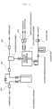
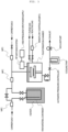
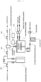
- the apparatus is not limited to such a single-substrate type apparatus including a film formation chamber as illustrated in each of FIG. 1 and FIG. 2 , and an apparatus capable of simultaneously processing a large number of substrates through use of a batch furnace may also be used.
- the method of producing a thin-film of the present invention includes: a step 1 (precursor thin-film formation step) of, in a film formation chamber (hereinafter sometimes referred to as "deposition reaction portion") having a substrate set therein, causing a raw material gas obtained by vaporizing the thin-film forming raw material to adsorb to the surface of the substrate to form a precursor thin-film; a step 2 (evacuation step) of evacuating the raw material gas remaining unreacted; and a step 3 (zirconium-containing thin-film formation step) of introducing a reactive gas into the film formation chamber to cause the precursor thin-film to react with the reactive gas at a temperature of 240°C or more and 450°C or less, to thereby form a zirconium-containing thin-film on the surface of the substrate.
- the method of producing a thin-film of the present invention preferably includes, after the step 3, a step 4 (evacuation step) of evacuating the gas in the film formation chamber.
- the method of producing a thin-film of the present invention when deposition performed by a series of operations of the step 1 (precursor thin-film formation step), the step 2 (evacuation step), the step 3 (zirconium-containing thin-film formation step), and the step 4 (evacuation step) in the stated order is defined as one cycle, and the cycle is repeated a plurality of times, the thickness of the thin-film can be controlled.
- the steps of the method of producing a thin-film of the present invention are described below.
- the step 1 is a step of introducing a raw material gas obtained by vaporizing the thin-film forming raw material into a film formation chamber having a substrate set therein to cause the raw material gas to adsorb to the surface of the substrate, to thereby form a precursor thin-film.
- raw material container a gas transportation method involving heating and/or decompressing the thin-film forming raw material in a container in which the raw material is stored (hereinafter referred to as "raw material container"), to thereby vaporize the thin-film forming raw material to obtain a raw material gas, and introducing the raw material gas into the film formation chamber having the substrate set therein together with a carrier gas, such as argon, nitrogen, or helium, as required as illustrated in each of FIG. 1 and FIG.
- carrier gas such as argon, nitrogen, or helium
- the zirconium compound represented by the general formula (1) itself may be used as the thin-film forming raw material.
- the zirconium compound represented by the general formula (1) or a solution obtained by dissolving the zirconium compound in an organic solvent may be used as the thin-film forming raw material.
- Such thin-film forming raw material may further contain a nucleophilic reagent or the like.
- the thin-film forming raw material is preferably vaporized in the range of 0°C or more and 200°C or less.
- a pressure in the raw material container and a pressure in the vaporization chamber are each preferably 1 Pa or more and 10,000 Pa or less.
- a material for the substrate to be set in the film formation chamber there are given, for example: silicon; ceramics, such as silicon nitride, titanium nitride, tantalum nitride, titanium oxide, ruthenium oxide, zirconium oxide, hafnium oxide, and lanthanum oxide; glass; and metals, such as metal cobalt and metal ruthenium.
- a shape of the substrate there are given, for example, a plate shape, a spherical shape, a fiber shape, and a scale-like shape.
- the surface of the substrate may be planar, or may have a three-dimensional structure such as a trench structure.
- the precursor thin-film can be formed on the surface of the substrate by causing the raw material gas to adsorb to the surface of the substrate.
- the substrate may be heated, or an inside of the film formation chamber may be heated.
- the conditions at the time of forming the precursor thin-film are not particularly limited, and for example, an adsorption temperature (substrate temperature), a system pressure, or the like may be appropriately determined depending on the kind of the thin-film forming raw material.
- the step 1 is preferably performed under a state in which the substrate is heated to 240°C or more and 450°C or less.
- the step 1 is more preferably performed under a state in which the substrate is heated to 250°C or more and 400°C or less, and the step is still more preferably performed under a state in which the substrate is heated to 300°C or more and 400°C or less.
- the system pressure is not particularly limited, but is preferably 1 Pa or more and 10,000 Pa or less. From the viewpoint that a uniform precursor thin-film is easily obtained, the system pressure is more preferably 10 Pa or more and 1,000 Pa or less.
- the degree of decompression in the case of performing decompression preferably falls within the range of 0.01 Pa or more and 300 Pa or less, and from the viewpoint that the evacuation of the raw material gas not having adsorbed is promoted, the degree of decompression more preferably falls within the range of 0.01 Pa or more and 100 Pa or less.
- the step 3 is a step of, after the step 2, introducing a reactive gas into the film formation chamber to cause the precursor thin-film, that is, the zirconium compound represented by the general formula (1), which has been deposited on the surface of the substrate, to react with the reactive gas through the action of the reactive gas and the action of heat, to thereby form a zirconium-containing thin-film.
- the reactive gas examples include: oxidizing gases, such as oxygen, ozone, nitrogen dioxide, nitrogen monoxide, water vapor, hydrogen peroxide, formic acid, acetic acid, and acetic anhydride; reducing gases such as hydrogen; and nitriding gases, such as organic amine compounds including a monoalkylamine, a dialkylamine, a trialkylamine, and an alkylenediamine, hydrazine, and ammonia. Those reactive gases may be used alone or as a mixture thereof.
- oxidizing gases such as oxygen, ozone, nitrogen dioxide, nitrogen monoxide, water vapor, hydrogen peroxide, formic acid, acetic acid, and acetic anhydride
- reducing gases such as hydrogen
- nitriding gases such as organic amine compounds including a monoalkylamine, a dialkylamine, a trialkylamine, and an alkylenediamine, hydrazine, and ammonia.
- Those reactive gases may be used alone
- the reactive gas is preferably an oxidizing gas, and from the viewpoint that reactivity between the precursor thin-film and the reactive gas becomes satisfactory, the reactive gas is more preferably a gas containing at least one selected from the group consisting of: oxygen; ozone; and water vapor.
- the oxidizing gas is used as the reactive gas, a zirconium oxide thin-film is formed as the zirconium-containing thin-film.
- a temperature (substrate temperature) at the time of causing the precursor thin-film to react with the reactive gas is 240°C or more and 450°C or less, and from the viewpoint that a high-quality thin-film more reduced in residual carbon is obtained, the temperature is preferably 250°C or more and 400°C or less, more preferably 300°C or more and 400°C or less.
- a pressure in the film formation chamber at the time of performing this step is preferably 1 Pa or more and 10,000 Pa or less, and from the viewpoint that reactivity between the precursor thin-film and the reactive gas becomes satisfactory, the pressure is more preferably 10 Pa or more and 1,000 Pa or less.
- the step 4 is a step of, after the step 3, evacuating the reactive gas remaining unreacted and a by-product gas from the film formation chamber in order to produce a high-quality thin-film.
- this step it is ideal that the reactive gas and the by-product gas be completely evacuated from the film formation chamber, but it is not always required that the gases be completely evacuated.
- An evacuation method and the degree of decompression in the case of performing decompression are the same as those in the above-mentioned step 2.
- the film thickness of the zirconium-containing thin-film to be obtained can be controlled by the number of the cycles.
- energy such as plasma, light, or a voltage
- a catalyst may be used therein.
- the timing at which the energy is applied and the timing at which the catalyst is used are not particularly limited.
- the energy may be applied or the catalyst may be used, for example, at the time of the introduction of the raw material gas into the film formation chamber or at the time of the heating in forming the precursor thin-film in the step 1, at the time of the introduction of the reactive gas into the film formation chamber or at the time of causing the reactive gas and the precursor thin-film to react with each other in the step 3, at the time of the evacuation of the system in the step 2 or 4, or between the above-mentioned respective steps.
- annealing treatment may be performed under an inert atmosphere, under an oxidizing atmosphere, or under a reducing atmosphere in order that more satisfactory electrical characteristics may be obtained.
- a reflow step may be provided.
- a temperature in this case is preferably 200°C or more and 1,000°C or less, and from the viewpoint that damage to the thin-film or the substrate caused by heat can be suppressed, the temperature is more preferably 250°C or more and 600°C or less.
- the thin-film to be produced by the method of producing a thin-film of the present invention can be provided as a desired kind of thin-film by appropriately selecting the other precursor, the reactive gas, and the production conditions, to thereby coat the substrate made of, for example, a metal, an oxide ceramic, a nitride ceramic, or glass.
- the thin-film of the present invention is excellent in electrical characteristics and optical characteristics, and hence can be widely used in the production of, for example, an electrode material for a memory element typified by a DRAM element, a resistance film, a diamagnetic film used in the recording layer of a hard disk, and a catalyst material for a polymer electrolyte fuel cell.
- a thin-film was produced on a silicon wafer serving as a substrate through use of the above-mentioned Zirconium Compound No. 1 as a thin-film forming raw material with the ALD apparatus of FIG. 1 under the following conditions and through the following steps.
- the composition of the thin-film was analyzed by X-ray photoelectron spectroscopy, it was recognized that the thin-film was a zirconium oxide thin-film, and a residual carbon content in the thin-film was less than 0.01 atm%, which was a detection limit.
Landscapes
- Chemical & Material Sciences (AREA)
- General Chemical & Material Sciences (AREA)
- Chemical Kinetics & Catalysis (AREA)
- Engineering & Computer Science (AREA)
- Materials Engineering (AREA)
- Mechanical Engineering (AREA)
- Metallurgy (AREA)
- Organic Chemistry (AREA)
- Inorganic Chemistry (AREA)
- Chemical Vapour Deposition (AREA)
- Inorganic Insulating Materials (AREA)
- Crystals, And After-Treatments Of Crystals (AREA)
- Superconductors And Manufacturing Methods Therefor (AREA)
- Formation Of Insulating Films (AREA)
Applications Claiming Priority (2)
| Application Number | Priority Date | Filing Date | Title |
|---|---|---|---|
| JP2020192293 | 2020-11-19 | ||
| PCT/JP2021/042093 WO2022107768A1 (ja) | 2020-11-19 | 2021-11-16 | 薄膜の製造方法 |
Publications (2)
| Publication Number | Publication Date |
|---|---|
| EP4249631A1 true EP4249631A1 (de) | 2023-09-27 |
| EP4249631A4 EP4249631A4 (de) | 2024-11-06 |
Family
ID=81709000
Family Applications (1)
| Application Number | Title | Priority Date | Filing Date |
|---|---|---|---|
| EP21894642.4A Pending EP4249631A4 (de) | 2020-11-19 | 2021-11-16 | Verfahren zur herstellung einer dünnschicht |
Country Status (8)
| Country | Link |
|---|---|
| US (1) | US20240018654A1 (de) |
| EP (1) | EP4249631A4 (de) |
| JP (2) | JPWO2022107768A1 (de) |
| KR (1) | KR102974029B1 (de) |
| CN (1) | CN116457918A (de) |
| IL (1) | IL302870A (de) |
| TW (1) | TWI920167B (de) |
| WO (1) | WO2022107768A1 (de) |
Family Cites Families (12)
| Publication number | Priority date | Publication date | Assignee | Title |
|---|---|---|---|---|
| JPS499804B1 (de) | 1968-08-30 | 1974-03-06 | ||
| US6274195B1 (en) | 1999-04-30 | 2001-08-14 | Postech Foundation | Organometallic complex process for the preparation thereof and metal organic chemical vapor deposition using same |
| JP4472338B2 (ja) * | 2001-10-26 | 2010-06-02 | シグマ−アルドリッチ・カンパニー | 化学気相成長のための改良された前駆体 |
| US20060014384A1 (en) * | 2002-06-05 | 2006-01-19 | Jong-Cheol Lee | Method of forming a layer and forming a capacitor of a semiconductor device having the same layer |
| WO2005063685A1 (ja) * | 2003-12-25 | 2005-07-14 | Asahi Denka Co., Ltd. | 金属化合物、薄膜形成用原料及び薄膜の製造方法 |
| JP2007088113A (ja) * | 2005-09-21 | 2007-04-05 | Sony Corp | 半導体装置の製造方法 |
| KR20110006450A (ko) * | 2009-07-14 | 2011-01-20 | 삼성전자주식회사 | 반도체 소자의 유전 박막 형성 방법 |
| KR101476016B1 (ko) * | 2010-01-07 | 2014-12-23 | 우베 고산 가부시키가이샤 | 금속 알콕사이드 화합물 및 당해 화합물을 사용한 금속 함유 박막의 제조법 |
| JP5675458B2 (ja) * | 2011-03-25 | 2015-02-25 | 東京エレクトロン株式会社 | 成膜方法、成膜装置および記憶媒体 |
| JP6760822B2 (ja) * | 2016-11-08 | 2020-09-23 | 株式会社Adeka | 化合物、薄膜形成用原料、原子層堆積法用の薄膜形成用原料及び薄膜の製造方法 |
| EP3677585A4 (de) * | 2017-08-30 | 2021-04-28 | Adeka Corporation | Metallalkoxidverbindung, dünnschichtbildendes rohmaterial und dünnschichtherstellungsverfahren |
| JP7149794B2 (ja) | 2018-09-28 | 2022-10-07 | 東京エレクトロン株式会社 | 半導体装置の製造方法 |
-
2021
- 2021-11-16 WO PCT/JP2021/042093 patent/WO2022107768A1/ja not_active Ceased
- 2021-11-16 CN CN202180077618.6A patent/CN116457918A/zh active Pending
- 2021-11-16 JP JP2022563773A patent/JPWO2022107768A1/ja active Pending
- 2021-11-16 EP EP21894642.4A patent/EP4249631A4/de active Pending
- 2021-11-16 US US18/036,975 patent/US20240018654A1/en active Pending
- 2021-11-16 KR KR1020237019211A patent/KR102974029B1/ko active Active
- 2021-11-16 IL IL302870A patent/IL302870A/en unknown
- 2021-11-18 TW TW110142880A patent/TWI920167B/zh active
-
2026
- 2026-04-23 JP JP2026071208A patent/JP2026120792A/ja active Pending
Also Published As
| Publication number | Publication date |
|---|---|
| JPWO2022107768A1 (de) | 2022-05-27 |
| WO2022107768A1 (ja) | 2022-05-27 |
| IL302870A (en) | 2023-07-01 |
| JP2026120792A (ja) | 2026-07-22 |
| KR20230107612A (ko) | 2023-07-17 |
| US20240018654A1 (en) | 2024-01-18 |
| TWI920167B (zh) | 2026-04-01 |
| TW202229605A (zh) | 2022-08-01 |
| KR102974029B1 (ko) | 2026-06-05 |
| EP4249631A4 (de) | 2024-11-06 |
| CN116457918A (zh) | 2023-07-18 |
Similar Documents
| Publication | Publication Date | Title |
|---|---|---|
| EP3783130A1 (de) | Quellenmaterial für dünnschichtbildung für atomlagenabscheidung und verfahren zur herstellung einer dünnschicht | |
| EP3677585A1 (de) | Metallalkoxidverbindung, dünnschichtbildendes rohmaterial und dünnschichtherstellungsverfahren | |
| US20250109296A1 (en) | Thin-film forming raw material used in atomic layer deposition method and method of producing thin-film | |
| US20240167154A1 (en) | Thin-film forming raw material, which is used in atomic layer deposition method, thin-film, method of producing thin-film, and zinc compound | |
| US12415821B2 (en) | Tin compound, thin-film forming raw material containing said compound, thin film formed from said thin-film forming raw material, method of producing said thin film using said compound as precursor, and method of producing said thin film | |
| US12104245B2 (en) | Compound, thin-film forming raw material that contains said compound, and method of manufacturing thin film | |
| EP4130010B1 (de) | Zinkverbindung, rohmaterial zur dünnschichtbildung, dünnschicht und verfahren zur herstellung einer dünnschicht | |
| US20230304154A1 (en) | Alkoxide compound, thin-film forming raw material, and method of producing thin-film | |
| EP4067365B1 (de) | Verbindung, dünnschichtbildendes material und verfahren zum produzieren einer dünnschicht | |
| US20240018654A1 (en) | Method of producing thin-film | |
| EP4249629A1 (de) | Verfahren zur herstellung einer dünnschicht | |
| EP3951006A1 (de) | Rohmaterial zur formung einer dünnschicht, verfahren zur herstellung einer dünnschicht und scandiumverbindung | |
| US12486573B2 (en) | Thin-film forming raw material, thin-film and method of producing thin-film | |
| EP4434994A1 (de) | Dünnfilmbildendes material zur verwendung bei der atomlagenabscheidung, dünnfilm, verfahren zur herstellung eines dünnfilms und rutheniumverbindung | |
| US12509764B2 (en) | Thin-film forming raw material used in atomic layer deposition method, and method of producing thin-film | |
| US20250154648A1 (en) | Precursor for forming metal thin film, manufacturing method using the same, and metal thin film manufactured thereby | |
| JP6704808B2 (ja) | 薄膜形成用原料及び薄膜の製造方法 | |
| US12577660B2 (en) | Compound, thin-film forming raw material, thin-film, and method of producing thin-film | |
| US12559839B2 (en) | Indium compound, thin-film forming raw material, thin film, and method of producing same | |
| KR20250155913A (ko) | 박막 형성용 조성물, 박막 형성용 조성물의 제조 방법, 박막 및 박막의 제조 방법 | |
| CN116529416A (zh) | 薄膜的制造方法 |
Legal Events
| Date | Code | Title | Description |
|---|---|---|---|
| STAA | Information on the status of an ep patent application or granted ep patent |
Free format text: STATUS: THE INTERNATIONAL PUBLICATION HAS BEEN MADE |
|
| PUAI | Public reference made under article 153(3) epc to a published international application that has entered the european phase |
Free format text: ORIGINAL CODE: 0009012 |
|
| STAA | Information on the status of an ep patent application or granted ep patent |
Free format text: STATUS: REQUEST FOR EXAMINATION WAS MADE |
|
| 17P | Request for examination filed |
Effective date: 20230511 |
|
| AK | Designated contracting states |
Kind code of ref document: A1 Designated state(s): AL AT BE BG CH CY CZ DE DK EE ES FI FR GB GR HR HU IE IS IT LI LT LU LV MC MK MT NL NO PL PT RO RS SE SI SK SM TR |
|
| DAV | Request for validation of the european patent (deleted) | ||
| DAX | Request for extension of the european patent (deleted) | ||
| A4 | Supplementary search report drawn up and despatched |
Effective date: 20241009 |
|
| RIC1 | Information provided on ipc code assigned before grant |
Ipc: H01L 21/02 20060101ALI20241002BHEP Ipc: C23C 16/455 20060101ALI20241002BHEP Ipc: H01L 21/316 20060101ALI20241002BHEP Ipc: H01L 21/31 20060101ALI20241002BHEP Ipc: C23C 16/40 20060101AFI20241002BHEP |