EP4254529A1 - Module de cellules solaires en pérovskite et son procédé de fabrication - Google Patents
Module de cellules solaires en pérovskite et son procédé de fabrication Download PDFInfo
- Publication number
- EP4254529A1 EP4254529A1 EP21898327.8A EP21898327A EP4254529A1 EP 4254529 A1 EP4254529 A1 EP 4254529A1 EP 21898327 A EP21898327 A EP 21898327A EP 4254529 A1 EP4254529 A1 EP 4254529A1
- Authority
- EP
- European Patent Office
- Prior art keywords
- charge transport
- separated
- electrode
- layer
- transport layer
- Prior art date
- Legal status (The legal status is an assumption and is not a legal conclusion. Google has not performed a legal analysis and makes no representation as to the accuracy of the status listed.)
- Pending
Links
Images














Classifications
-
- H—ELECTRICITY
- H10—SEMICONDUCTOR DEVICES; ELECTRIC SOLID-STATE DEVICES NOT OTHERWISE PROVIDED FOR
- H10K—ORGANIC ELECTRIC SOLID-STATE DEVICES
- H10K30/00—Organic devices sensitive to infrared radiation, light, electromagnetic radiation of shorter wavelength or corpuscular radiation
- H10K30/80—Constructional details
-
- C—CHEMISTRY; METALLURGY
- C07—ORGANIC CHEMISTRY
- C07F—ACYCLIC, CARBOCYCLIC OR HETEROCYCLIC COMPOUNDS CONTAINING ELEMENTS OTHER THAN CARBON, HYDROGEN, HALOGEN, OXYGEN, NITROGEN, SULFUR, SELENIUM OR TELLURIUM
- C07F7/00—Compounds containing elements of Groups 4 or 14 of the Periodic Table
- C07F7/24—Lead compounds
-
- H—ELECTRICITY
- H10—SEMICONDUCTOR DEVICES; ELECTRIC SOLID-STATE DEVICES NOT OTHERWISE PROVIDED FOR
- H10K—ORGANIC ELECTRIC SOLID-STATE DEVICES
- H10K30/00—Organic devices sensitive to infrared radiation, light, electromagnetic radiation of shorter wavelength or corpuscular radiation
- H10K30/10—Organic devices sensitive to infrared radiation, light, electromagnetic radiation of shorter wavelength or corpuscular radiation comprising heterojunctions between organic semiconductors and inorganic semiconductors
- H10K30/15—Sensitised wide-bandgap semiconductor devices, e.g. dye-sensitised TiO2
-
- H—ELECTRICITY
- H10—SEMICONDUCTOR DEVICES; ELECTRIC SOLID-STATE DEVICES NOT OTHERWISE PROVIDED FOR
- H10K—ORGANIC ELECTRIC SOLID-STATE DEVICES
- H10K30/00—Organic devices sensitive to infrared radiation, light, electromagnetic radiation of shorter wavelength or corpuscular radiation
- H10K30/40—Organic devices sensitive to infrared radiation, light, electromagnetic radiation of shorter wavelength or corpuscular radiation comprising a p-i-n structure, e.g. having a perovskite absorber between p-type and n-type charge transport layers
-
- H—ELECTRICITY
- H10—SEMICONDUCTOR DEVICES; ELECTRIC SOLID-STATE DEVICES NOT OTHERWISE PROVIDED FOR
- H10K—ORGANIC ELECTRIC SOLID-STATE DEVICES
- H10K39/00—Integrated devices, or assemblies of multiple devices, comprising at least one organic radiation-sensitive element covered by group H10K30/00
- H10K39/10—Organic photovoltaic [PV] modules; Arrays of single organic PV cells
- H10K39/12—Electrical configurations of PV cells, e.g. series connections or parallel connections
-
- H—ELECTRICITY
- H10—SEMICONDUCTOR DEVICES; ELECTRIC SOLID-STATE DEVICES NOT OTHERWISE PROVIDED FOR
- H10K—ORGANIC ELECTRIC SOLID-STATE DEVICES
- H10K85/00—Organic materials used in the body or electrodes of devices covered by this subclass
-
- H—ELECTRICITY
- H10—SEMICONDUCTOR DEVICES; ELECTRIC SOLID-STATE DEVICES NOT OTHERWISE PROVIDED FOR
- H10K—ORGANIC ELECTRIC SOLID-STATE DEVICES
- H10K85/00—Organic materials used in the body or electrodes of devices covered by this subclass
- H10K85/50—Organic perovskites; Hybrid organic-inorganic perovskites [HOIP], e.g. CH3NH3PbI3
-
- Y—GENERAL TAGGING OF NEW TECHNOLOGICAL DEVELOPMENTS; GENERAL TAGGING OF CROSS-SECTIONAL TECHNOLOGIES SPANNING OVER SEVERAL SECTIONS OF THE IPC; TECHNICAL SUBJECTS COVERED BY FORMER USPC CROSS-REFERENCE ART COLLECTIONS [XRACs] AND DIGESTS
- Y02—TECHNOLOGIES OR APPLICATIONS FOR MITIGATION OR ADAPTATION AGAINST CLIMATE CHANGE
- Y02E—REDUCTION OF GREENHOUSE GAS [GHG] EMISSIONS, RELATED TO ENERGY GENERATION, TRANSMISSION OR DISTRIBUTION
- Y02E10/00—Energy generation through renewable energy sources
- Y02E10/50—Photovoltaic [PV] energy
- Y02E10/549—Organic PV cells
-
- Y—GENERAL TAGGING OF NEW TECHNOLOGICAL DEVELOPMENTS; GENERAL TAGGING OF CROSS-SECTIONAL TECHNOLOGIES SPANNING OVER SEVERAL SECTIONS OF THE IPC; TECHNICAL SUBJECTS COVERED BY FORMER USPC CROSS-REFERENCE ART COLLECTIONS [XRACs] AND DIGESTS
- Y02—TECHNOLOGIES OR APPLICATIONS FOR MITIGATION OR ADAPTATION AGAINST CLIMATE CHANGE
- Y02P—CLIMATE CHANGE MITIGATION TECHNOLOGIES IN THE PRODUCTION OR PROCESSING OF GOODS
- Y02P70/00—Climate change mitigation technologies in the production process for final industrial or consumer products
- Y02P70/50—Manufacturing or production processes characterised by the final manufactured product
Definitions
- the present disclosure relates generally to a perovskite solar cell module and a manufacturing method for the same and, more particularly, to a perovskite solar cell module and a manufacturing method for the same capable of improving the reliability of the perovskite solar cell module.
- Perovskite is a semiconductor material with a special hexagonal structure, and has the property of converting light into electricity (photoelectric conversion) or electricity into light (luminescence). Due to its low production cost and high efficiency, perovskite is attracting attention as a next-generation solar cell material. Solar cells are a renewable and eco-friendly source of energy, and are considered as a prominent energy source that can solve the problems of limited reserves and environmental pollution caused by conventional fossil fuels.
- perovskite solar cells are under active development because they can realize high efficiency at a lower cost than conventional silicon solar cells.
- the voltage and current values that can be obtained from one small perovskite solar cell are limited, and it is difficult to apply it for power generation to commonly used mobile phones or LED electronic devices.
- large-area modularization is essential for commercialization of perovskite.
- increasing the area of the solar cell results in an increase in sheet resistance and consequently a reduction in efficiency, which is problematic.
- modularization has to be achieved by connecting a plurality of small-sized solar cells.
- perovskite due to inherent nature of perovskite, when moisture and oxygen permeate into perovskite, the crystal structure of perovskite is deformed. This may cause deformation and damage to the interface of the solar cell, resulting in deterioration in performance.
- an objective of the present disclosure is to provide a perovskite solar cell module capable of improving module stability by blocking permeation of external moisture and oxygen into the module and preventing performance degradation by minimizing contact resistance and interfacial resistance caused by series connection of small solar cells, and to provide a manufacturing method for the same.
- the present disclosure provides a perovskite solar cell module including a plurality of perovskite solar cells disposed on a substrate.
- Each of the perovskite solar cells may include: a first electrode; a first charge transport layer stacked on the first electrode; a photoactive layer stacked on the first charge transport layer and made of a perovskite material; a second charge transport layer stacked on the photoactive layer; and a second electrode stacked on the second charge transport layer,
- the second electrode of each cell may be electrically connected in series to the first electrode of a nearest cell.
- the second electrode of each cell may be stacked on an upper surface of the second charge transport layer and in contact with the first electrode of the nearest cell, and be patterned to be separated from the second electrode of the nearest cell.
- each cell may further include a functional layer stacked on at least one of positons between the second charge transport layer and the second electrode thereof, and between first charge transport layers, photoactive layers, and second charge transport layers patterned and separated so that the second electrode of each cell is in contact with the first electrode of the nearest cell, the functional layer being configured to block permeation of external moisture and oxygen.
- each cell may further include a functional layer stacked on at least one of an upper surface of the second electrode thereof and between the second electrodes patterned and separated in neighboring cells.
- the second electrode of each cell may be stacked on the upper surface of the second charge transport layer and in contact with the first electrode of the nearest cell, and the first charge transport layer, the photoactive layer, the second charge transport layer, the functional layer, and the second electrode of each cell may be patterned on the first electrode by etching to be separated from the first charge transport layer, the photoactive layer, the second charge transport layer, the functional layer, and the second electrode of the nearest cell.
- each cell may further include a functional layer stacked on at least one of an upper surface of the second electrode thereof and between the first charge transport layers, the photoactive layers, the second charge transport layers, the functional layers, and the second electrodes patterned and separated in neighboring cells.
- a functional layer stacked on at least one of an upper surface of the second electrode thereof and between the first charge transport layers, the photoactive layers, the second charge transport layers, the functional layers, and the second electrodes patterned and separated in neighboring cells.
- each cell may further include a functional layer stacked on at least one of an upper surface of the second electrode thereof and between the second electrodes patterned and separated in neighboring cells.
- the second electrode of each cell may be stacked on the upper surface of the second charge transport layer and in contact with the first electrode of the nearest cell, and the first charge transport layer, the photoactive layer, the second charge transport layer, and the second electrode of each cell may be patterned on the first electrode by etching to be separated from the first charge transport layer, the photoactive layer, the second charge transport layer, and the second electrode of the nearest cell.
- each cell may further include a functional layer stacked on at least one of an upper surface of the second electrode thereof and between the first charge transport layers, the photoactive layers, the second charge transport layers, and the second electrodes patterned and separated in neighboring cells.
- a method of manufacturing a perovskite solar cell module in which a plurality of perovskite solar cells are disposed on a substrate.
- the method may include a first pattern forming step of sequentially stacking a first electrode, a first charge transport layer, a photoactive layer, and a second charge transport layer on the substrate, and patterning the first charge transport layer, the photoactive layer, and the second charge transport layer to separate each of the layers with predetermined spaces formed therein so that a second electrode of each cell is in contact with the first electrode of a nearest cell.
- the method may further include a second pattern forming step of stacking a functional layer on an upper surface of the second charge transport layer of each cell and between the second charge transport layer and the second electrode of each cell, and partially patterning the functional layer to form predetermined spaces therein so that the second electrode of each cell is electrically connected in series to the first electrode of the nearest cell.
- the method may further include a third pattern forming step of patterning the second electrode to form predetermined spaces therein so that the second electrode of each cell is separated from the second electrode of the nearest cell.
- a perovskite solar cell module including: a substrate; first electrodes formed to be spaced apart from each other on an upper surface of the substrate, or stacked on the upper surface of the substrate and patterned to be separated with predetermined spaces formed therein; a first charge transport layer stacked on an upper surface of the first electrode and patterned to be separated with predetermined spaces formed therein; a photoactive layer stacked on an upper surface of the first charge transport layer and patterned to be separated with predetermined spaces formed therein; a second charge transport layer stacked on an upper surface of the photoactive layer and patterned to be separated with predetermined spaces formed therein; a functional layer stacked on an upper surface of the second charge transport layer and between the separated first charge transport layers, the separated photoactive layers, and the separated second charge transport layers, the functional layer being configured to reduce interfacial resistance and block permeation of external moisture and oxygen; and a second electrode formed on an upper surface of the functional layer and patterned to be separated with predetermined spaces formed therein.
- each of the separated second electrodes may be formed adjacent to or in contact with an adjacent first electrode and be electrically connected to the adjacent first electrode.
- the functional layer may be formed on a surface of each of the separated second electrodes and be stacked at least between the separated second electrodes.
- the first charge transport layer, the photoactive layer, the second charge transport layer, the functional layer, and the second electrode may be patterned on the first electrodes to be separated with predetermined spaces formed therein.
- the functional layer may be formed between the separated first charge transport layers, the separated photoactive layers, the separated second charge transport layers, the separated functional layers, and the separated second electrodes.
- a perovskite solar cell module including: a substrate; first electrodes formed to be spaced apart from each other on an upper surface of the substrate, or stacked on the upper surface of the substrate and patterned to be separated with predetermined spaces formed therein; a first charge transport layer stacked on an upper surface of the first electrode and patterned to be separated with predetermined spaces formed therein; a photoactive layer stacked on an upper surface of the first charge transport layer and patterned to be separated with predetermined spaces formed therein; a second charge transport layer stacked on an upper surface of the photoactive layer and patterned to be separated with predetermined spaces formed therein; a functional layer stacked between the separated first charge transport layers, the separated photoactive layers, and the separated second charge transport layers, the functional layer being configured to reduce interfacial resistance and block permeation of external moisture and oxygen; and a second electrode formed on an upper surface of the second charge transport layer and an upper surface of the functional layer and patterned to be separated with predetermined spaces formed therein.
- each of the separated second electrodes may be formed adjacent to or in contact with an adjacent first electrode and be electrically connected to the adjacent first electrode.
- the functional layer may be formed on a surface of each of the separated second electrodes and be stacked at least between the separated second electrodes.
- the first charge transport layer, the photoactive layer, the second charge transport layer, the functional layer, and the second electrode may be patterned on the first electrodes to be separated with predetermined spaces formed therein.
- the functional layer may be formed between the separated first charge transport layers, the separated photoactive layers, the separated second charge transport layers, the separated functional layers, and the separated second electrodes.
- a perovskite solar cell module including: a substrate; first electrodes formed to be spaced apart from each other on an upper surface of the substrate, or stacked on the upper surface of the substrate and patterned to be separated with predetermined spaces formed therein; a first charge transport layer stacked on an upper surface of the first electrode and patterned to be separated with predetermined spaces formed therein; a photoactive layer stacked on an upper surface of the first charge transport layer and patterned to be separated with predetermined spaces formed therein; a second charge transport layer stacked on an upper surface of the photoactive layer and patterned to be separated with predetermined spaces formed therein; a second electrode stacked on an upper surface of the second charge transport layer and between the separated first charge transport layers, the separated photoactive layers, and the separated second charge transport layers, and patterned to be separated with predetermined spaced formed therein; and a functional layer formed on a surface of each of the separated second electrodes and stacked at least between the separated second electrodes, and configured to reduce interfa
- each of the separated second electrodes may be formed adjacent to or in contact with an adjacent first electrode and be electrically connected to the adjacent first electrode.
- the first charge transport layer, the photoactive layer, the second charge transport layer, the functional layer, and the second electrode may be patterned on the first electrodes to be separated with predetermined spaces formed therein.
- the functional layer may be formed on a surface of each of the separated second electrodes, and be stacked at least between the separated first charge transport layers, the separated photoactive layers, the separated second charge transport layers, the separated functional layers, and the separated second electrodes.
- a perovskite solar cell module including a substrate, a first electrode, a first charge transport layer, a photoactive layer, a second charge transport layer, and a second electrode, by stacking a functional layer in predetermined spaces between separated first charge transport layers, separated photoactive layers, and separated second charge transport layers patterned on separated first electrodes, it is possible to prevent penetration of external moisture and oxygen and reduce interfacial resistance and contact resistance caused by electric connection, thereby improving photoelectric conversion efficiency.
- the perovskite solar cell module includes a substrate 110, a first electrode 120, a first charge transport layer 130, a photoactive layer 140, a second charge transport layer 150, a second electrode 160, and functional layers 150a and 150b.
- Each embodiment provides a perovskite solar cell module that is modified according to a structural change, and the position and shape of the functional layers 150a and 150b.
- FIG. 1 is a schematic view illustrating a manufacturing sequence of a perovskite solar cell module according to an embodiment.
- the perovskite solar cell module is manufactured in the following manner.
- a first electrode 120 is formed on an upper surface of a substrate 110, and then the first electrode 120 is patterned through physical and chemical removal, such as dry etching, wet etching, laser, and mechanical processing, to be separated with first spaces a1 formed therein.
- a first charge transport layer 130, a photoactive layer 140, and a second charge transport layer 150 are sequentially stacked on upper surfaces of the separated first electrodes 120.
- the first charge transport layer 130, the photoactive layer 140, and the second charge transport layer 150 stacked on the separated first electrodes 120 are patterned through physical and chemical removal, such as dry etching, wet etching, laser, and mechanical processing, to be separated with second spaces a2 formed therein.
- a second electrode 160 is stacked.
- the second electrode 160 is stacked on upper surfaces of the separated second charge transport layers 150 and in the second spaces a2 formed on the separated first electrodes 120.
- the second electrode 160 is patterned through physical and chemical removal, such as dry etching, wet etching, laser, and mechanical processing, to be separated with third spaces a3 formed therein.
- the width of the first spaces a1, the second spaces a2, and the third spaces a3 may be in the range of 0.01 um to 150 um.
- Each separated second electrode 160 is formed to be in contact with an upper surface of an adjacent first electrode 120 and is electrically connected to the adjacent first electrode 120 to form the perovskite solar cell module.
- the substrate 110 may be made of a material selected from the group consisting of glass, polyethylene terephthalate (PET), polyethylene naphthalate (PEN), polyethersulfone (PES), polyimide (PI), crystalline silicon, and amorphous silicon, but is not limited thereto.
- PET polyethylene terephthalate
- PEN polyethylene naphthalate
- PES polyethersulfone
- PI polyimide
- crystalline silicon crystalline silicon
- amorphous silicon but is not limited thereto.
- the first electrode 120 and the second electrode 160 may be composed of at least one layer.
- the first electrode 120 and the second electrode 160 may be made of a material selected from the group consisting of indium tin oxide (ITO), fluorine-doped tin oxide (FTO), indium zinc oxide (IZO), aluminum zinc oxide (AZO), molybdenum trioxide (MoO 3 ), tungsten trioxide (WoO 3 ), indium gallium zinc oxide (IGZO), indium zinc-tin oxide (IZTO), metal NWs (silver nanowires, copper nanowires, etc.), carbon, graphene, reduced grapheme oxide (r-GO), PEDOT:PSS, aluminum (Al), silver (Ag), copper(Cu), and gold (Au), but are not limited thereto.
- ITO indium tin oxide
- FTO fluorine-doped tin oxide
- IZO indium zinc oxide
- AZO aluminum zinc oxide
- MoO 3 molybdenum tri
- Each of the first charge transport layer 130 and the second charge transport layer 150 may be provided as at least one layer, and may be made of any one of materials having electron transport, hole transport, electron blocking, and hole blocking functions.
- the materials having the function of electron transport, electron blocking, hole transport, and hole blocking are defined by a role according to the energy level of the materials, and the first charge transport layer 130 and the second charge transport layer 150 may be made of materials having opposite functions.
- the second charge transport layer 150 may be made of a material having a hole transport function.
- the present disclosure is not limited thereto, and the first charge transport layer 130 may be made of a material having a hole transport function, and the second charge transport layer 150 may be made of a material having an electron transport function.
- each of the first charge transport layer 130 and the second charge transport layer 150 is provided as at least one layer
- a material having a hole blocking function may be additionally provided
- a material having an electron blocking function may be additionally provided.
- the photoactive layer 140 is made of a material having a chemical composition of AMX 3 .
- A may be at least one metal element or organic compound
- M may be any one of metal atoms
- X may be an oxide or a combination of any one or more of halogen atoms of chlorine (Cl), bromine (Br), and iodine (I).
- the A atom is located at each vertex of a cubic unit cell
- the M atom is located at the body-center position, that is, the center of the body of the cell
- the X atom is located at the face-center position, that is, the center of each face of the cell.
- Representative examples include CH 3 NHPbI 3 (methylammonium lead iodide, MAPbI 3 ) and HC(NH 2 ) 2 PbI 3 (formamidinium lead iodide, FAPbI 3 ).
- MAPbI 3 methylammonium lead iodide
- HC(NH 2 ) 2 PbI 3 formamidinium lead iodide, FAPbI 3
- each of the charge transport layers is defined by a role according to the energy level of the material thereof.
- a perovskite solar cell module according to each embodiment described below may further include functional layers 150a and 150b in addition to the substrate 110, the first electrode 120, the first charge transport layer 130, the photoactive layer 140, the second charge transport layer 150, and the second electrode 160.
- the functional layers 150a and 150b may be made of a non-metal-based material formed by combining at least one or more of hydrogen (H), carbon (C), nitrogen (N), oxygen (O), fluorine (F), neon (Ne), phosphorus (P), sulfur (S), chlorine (Cl), argon (Ar), selenium (Se), bromine (Br), krypton (Kr), iodine (I), xenon (Xe), radon (Rn), and astatine (At ), but are not limited thereto.
- Modified examples of the perovskite solar cell module according to the embodiment will be described in first to sixth embodiments.
- Each of the first to fourth embodiments will be described with reference to one schematic view and 23 exemplary views
- each of the fifth and sixth embodiments will be described with reference to one schematic view and seven exemplary views.
- the structure of modified examples of each embodiment may vary depending on a structural change of the above-described perovskite solar cell module including the first electrode 120, the first charge transport layer 130, the photoactive layer 140, the second charge transport layer 150, and the second electrode 160, and the position and shape of the functional layers 150a and 150b.
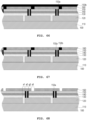
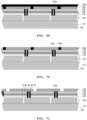
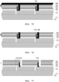
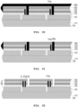
- a perovskite solar cell module according to the first embodiment will be described with reference to FIGS. 2 to 25 .
- a perovskite solar cell module according to the second embodiment will be described with reference to FIGS. 26 to 49 .
- a perovskite solar cell module according to the third embodiment will be described with reference to FIGS. 50 to 73 .
- a perovskite solar cell module according to the fourth embodiment will be described with reference to FIGS. 74 to 97 .
- a perovskite solar cell module according to the fifth embodiment will be described with reference to FIGS. 98 to 105 .
- a perovskite solar cell module according to the sixth embodiment will be described with reference to FIGS. 106 to 113 .
- FIG. 2 is a schematic view illustrating the perovskite solar cell module according to the first embodiment.
- the perovskite solar cell module 100 includes a substrate 110, a first electrode 120, a first charge transport layer 130, a photoactive layer 140, a second charge transport layer 150, a functional layer 150a, and a second electrode 160.
- the first electrode 120 is stacked on an upper surface of the substrate 110, and patterned through physical and chemical removal, such as dry etching, wet etching, laser, and mechanical processing, to be separated with first spaces a1 formed therein.
- the first charge transport layer 130, the photoactive layer 140, and the second charge transport layer 150 are sequentially stacked on upper surfaces of the separated first electrodes 120.
- the first charge transport layer 130, the photoactive layer 140, and the second charge transport layer 150 stacked on the separated first electrodes 120 are patterned through physical and chemical removal, such as dry etching, wet etching, laser, and mechanical processing, to be separated with second spaces a2 formed therein.
- the functional layer 150a is stacked on upper surfaces of the separated second charge transport layers 150 and in the second spaces a2 formed between the separated first charge transport layers 130, the separated photoactive layers 140, and the separated second charge transport layers 150.
- the second electrode 160 is stacked on an upper surface of the functional layer 150a.
- the second electrode 160 is patterned through physical and chemical removal, such as dry etching, wet etching, laser, and mechanical processing, to be separated with third spaces a3 formed therein.
- perovskite solar cell modules described in detail below that are modified from the first embodiment are configured in a manner similar to that described in FIG. 2 , a detailed description thereof will be omitted. However, when structural changes, modifications, and variations are made therein, a description thereof will be given.
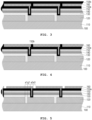
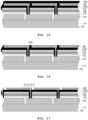
- FIGS. 3 to 13 are views illustrating other examples of the perovskite solar cell module according to the first embodiment illustrated in FIG. 2 .
- FIG. 3 is a view illustrating a first example of the perovskite solar cell module according to the first embodiment.
- the first example of the perovskite solar cell module according to the first embodiment including a substrate 110, a first electrode 120, a first charge transport layer 130, a photoactive layer 140, a second charge transport layer 150, a functional layer 150a, and a second electrode 160 further includes a functional layer 150b.
- the functional layer 150b is formed on a surface of each of separated second electrodes 160, and is stacked on upper surfaces of the separated second electrodes 160 and in third spaces a3 formed between the separated second electrodes 160.
- FIG. 4 is a view illustrating a second example of the perovskite solar cell module according to the first embodiment.
- the second example of the perovskite solar cell module according to the first embodiment including a substrate 110, a first electrode 120, a first charge transport layer 130, a photoactive layer 140, a second charge transport layer 150, a functional layer 150a, and a second electrode 160 further includes a functional layer 150b.
- the functional layer 150b is formed on a surface of each of separated second electrodes 160, and is stacked in third spaces a3 formed between the separated second electrodes 160.
- FIG. 5 is a view illustrating a third example of the perovskite solar cell module according to the first embodiment.
- the third example of the perovskite solar cell module according to the first embodiment includes a substrate 110, a first electrode 120, a first charge transport layer 130, a photoactive layer 140, a second charge transport layer 150, a functional layer 150a, and a second electrode 160.
- the first charge transport layer 130, the photoactive layer 140, and the second charge transport layer 150 are stacked on separated first electrodes 120 and patterned through physical and chemical removal, such as dry etching, wet etching, laser, and mechanical processing, to be separated with second spaces a2 formed therein.
- the first charge transport layer 130, the photoactive layer 140, and the second charge transport layer 150 are patterned so that a first gap g1 exists between a first space a1 and a second space a2.
- Perovskite solar cell modules modified from the third example of the perovskite solar cell module according to the first embodiment described above with reference to FIG. 5 will be described with reference to FIGS. 6 and 7 .
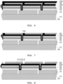
- FIG. 6 is a view illustrating a fourth example of the perovskite solar cell module according to the first embodiment.
- the fourth example of the perovskite solar cell module according to the first embodiment including a substrate 110, a first electrode 120, a first charge transport layer 130, a photoactive layer 140, a second charge transport layer 150, a functional layer 150a, and a second electrode 160 further includes a functional layer 150b.
- the functional layer 150b is formed on a surface of each of separated second electrodes 160, and is stacked on upper surfaces of the separated second electrodes 160 and in third spaces a3 formed between the separated second electrodes 160.
- FIG. 7 is a view illustrating a fifth example of the perovskite solar cell module according to the first embodiment.
- the fifth example of the perovskite solar cell module according to the first embodiment including a substrate 110, a first electrode 120, a first charge transport layer 130, a photoactive layer 140, a second charge transport layer 150, a functional layer 150a, and a second electrode 160 further includes a functional layer 150b.
- the functional layer 150b is formed on a surface of each of separated second electrodes 160, and is stacked in third spaces a3 formed between the separated second electrodes 160.
- FIG. 8 is a view illustrating a sixth example of the perovskite solar cell module according to the first embodiment.
- the sixth example of the perovskite solar cell module according to the first embodiment includes a substrate 110, a first electrode 120, a first charge transport layer 130, a photoactive layer 140, a second charge transport layer 150, a functional layer 150a, and a second electrode 160.
- the second electrode 160 is stacked on an upper surface of the functional layer 150a and patterned to be separated with third spaces a3 formed therein.
- the second electrode 160 is patterned so that a second gap g2 exists between a second space a2 and a third space a3.
- Perovskite solar cell modules modified from the sixth example of the perovskite solar cell module according to the first embodiment described above with reference to FIG. 8 will be described with reference to FIGS. 9 and 10 .
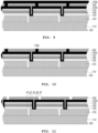
- FIG. 9 is a view illustrating a seventh example of the perovskite solar cell module according to the first embodiment.
- the seventh example of the perovskite solar cell module according to the first embodiment including a substrate 110, a first electrode 120, a first charge transport layer 130, a photoactive layer 140, a second charge transport layer 150, a functional layer 150a, and a second electrode 160 further includes a functional layer 150b.
- the functional layer 150b is formed on a surface of each of separated second electrodes 160, and is stacked on upper surfaces of the separated second electrodes 160 and in third spaces a3 formed between the separated second electrodes 160.
- FIG. 10 is a view illustrating an eighth example of the perovskite solar cell module according to the first embodiment.
- the eighth example of the perovskite solar cell module according to the first embodiment including a substrate 110, a first electrode 120, a first charge transport layer 130, a photoactive layer 140, a second charge transport layer 150, a functional layer 150a, and a second electrode 160 further includes a functional layer 150b.
- the functional layer 150b is formed on a surface of each of separated second electrodes 160, and is stacked in third spaces a3 formed between the separated second electrodes 160.
- FIG. 11 is a view illustrating a ninth example of the perovskite solar cell module according to the first embodiment.
- the ninth example of the perovskite solar cell module according to the first embodiment includes a substrate 110, a first electrode 120, a first charge transport layer 130, a photoactive layer 140, a second charge transport layer 150, a functional layer 150a, and a second electrode 160.
- the first charge transport layer 130, the photoactive layer 140, and the second charge transport layer 150 are stacked on separated first electrodes 120 and patterned through physical and chemical removal, such as dry etching, wet etching, laser, and mechanical processing, to be separated with second spaces a2 formed therein.
- the first charge transport layer 130, the photoactive layer 140, and the second charge transport layer 150 are patterned so that a first gap g1 exists between a first space a1 and a second space a2.
- the second electrode 160 is stacked on an upper surface of the functional layer 150a and patterned through physical and chemical removal, such as dry etching, wet etching, laser, and mechanical processing, to be separated with third spaces a3 formed therein.
- the second electrode 160 is patterned so that a second gap g2 exists between a second space a2 and a third space a3.
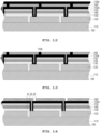
- Perovskite solar cell modules modified from the ninth example of the perovskite solar cell module according to the first embodiment described above with reference to FIG. 11 will be described with reference to FIGS. 12 and 13 .
- FIG. 12 is a view illustrating a tenth example of the perovskite solar cell module according to the first embodiment.
- the tenth example of the perovskite solar cell module according to the first embodiment including a substrate 110, a first electrode 120, a first charge transport layer 130, a photoactive layer 140, a second charge transport layer 150, a functional layer 150a, and a second electrode 160 further includes a functional layer 150b.
- the functional layer 150b is stacked on upper surfaces of separated second electrodes 160 and in third spaces a3 formed between the separated second electrodes 160.
- FIG. 13 is a view illustrating an eleventh example of the perovskite solar cell module according to the first embodiment.
- the eleventh example of the perovskite solar cell module according to the first embodiment including a substrate 110, a first electrode 120, a first charge transport layer 130, a photoactive layer 140, a second charge transport layer 150, a functional layer 150a, and a second electrode 160 further includes a functional layer 150b.
- the functional layer 150b is stacked in third spaces a3 formed between separated second electrodes 160.
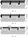
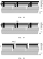
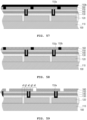
- FIGS. 14 to 25 are views illustrating modified structures of the first to eleventh examples of the perovskite solar cell module according to the first embodiment described above.
- a functional layer 150a is patterned through physical and chemical removal, such as dry etching, wet etching, laser, and mechanical processing, so that each second electrode 160 is in contact with and electrically connected to an adjacent first electrode 120.
- FIG. 26 is a schematic view illustrating a perovskite solar cell module according to a second embodiment.
- the perovskite solar cell module 100 includes a substrate 110, a first electrode 120, a first charge transport layer 130, a photoactive layer 140, a second charge transport layer 150, a functional layer 150a, and a second electrode 160.
- the first electrode 120 is stacked on an upper surface of the substrate 110, and patterned through physical and chemical removal, such as dry etching, wet etching, laser, and mechanical processing, to be separated with first spaces a1 formed therein.
- the first charge transport layer 130, the photoactive layer 140, and the second charge transport layer 150 are sequentially stacked on upper surfaces of the separated first electrodes 120.
- the first charge transport layer 130, the photoactive layer 140, and the second charge transport layer 150 stacked on the separated first electrodes 120 are patterned through physical and chemical removal, such as dry etching, wet etching, laser, and mechanical processing, to be separated with second spaces a2 formed therein.
- the functional layer 150a is stacked on upper surfaces of the separated second charge transport layers 150 and in the second spaces a2.
- the second electrode 160 is stacked on an upper surface of the functional layer 150a.
- the separated first charge transport layers 130, the separated photoactive layers 140, the separated second charge transport layers 150, the functional layer 150a, and the second electrode 160 stacked on the separated first electrodes 120 are patterned through physical and chemical removal, such as dry etching, wet etching, laser, and mechanical processing, to be separated with third spaces a3 formed therein.
- perovskite solar cell modules described in detail below that are modified from the second embodiment are configured in a manner similar to that described in FIG. 26 , a detailed description thereof will be omitted. However, when structural changes, modifications, and variations are made therein, a description thereof will be given.
- FIGS. 27 to 49 are views illustrating other examples of the perovskite solar cell module according to the second embodiment illustrated in FIG. 26 .
- FIG. 27 is a view illustrating a first example of the perovskite solar cell module according to the second embodiment.
- the first example of the perovskite solar cell module according to the second embodiment including a substrate 110, a first electrode 120, a first charge transport layer 130, a photoactive layer 140, a second charge transport layer 150, a functional layer 150a, and a second electrode 160 further includes a functional layer 150b.
- the functional layer 150b is formed on a surface of each of separated second electrodes 160, and is stacked on upper surfaces of the separated second electrodes 160 and in third spaces a3 formed between separated first charge transport layers 130, separated photoactive layers 140, separated second charge transport layers 150, separated functional layers 150a, and the separated second electrodes 160.
- FIG. 28 is a view illustrating a second example of the perovskite solar cell module according to the second embodiment.
- the second example of the perovskite solar cell module according to the second embodiment including a substrate 110, a first electrode 120, a first charge transport layer 130, a photoactive layer 140, a second charge transport layer 150, a functional layer 150a, and a second electrodes 160 further includes a functional layer 150b.
- the functional layer 150b is formed on a surface of each of separated second electrodes 160, and is stacked in third spaces a3 formed between separated first charge transport layers 130, separated photoactive layers 140, separated second charge transport layers 150, separated functional layers 150a, and the separated second electrodes 160.
- FIG. 29 is a view illustrating a third example of the perovskite solar cell module according to the second embodiment.
- the third example of the perovskite solar cell module according to the second embodiment includes a substrate 110, a first electrode 120, a first charge transport layer 130, a photoactive layer 140, a second charge transport layer 150, a functional layer 150a, and a second electrode 160.
- the first charge transport layer 130, the photoactive layer 140, and the second charge transport layer 150 are stacked on separated first electrodes 120 and patterned through physical and chemical removal, such as dry etching, wet etching, laser, and mechanical processing, to be separated with second spaces a2 formed therein.
- the first charge transport layer 130, the photoactive layer 140, and the second charge transport layer 150 are patterned so that a first gap g1 exists between a first space a1 and a second space a2.
- Perovskite solar cell modules modified from the third example of the perovskite solar cell module according to the second embodiment described above with reference to FIG. 29 will be described with reference to FIGS. 30 and 31 .
- FIG. 30 is a view illustrating a fourth example of the perovskite solar cell module according to the second embodiment.
- the fourth example of the perovskite solar cell module according to the second embodiment including a substrate 110, a first electrode 120, a first charge transport layer 130, a photoactive layer 140, a second charge transport layer 150, a functional layer 150a, and a second electrode 160 further includes a functional layer 150b.
- the functional layer 150b is formed on a surface of each of separated second electrodes 160, and is stacked on upper surfaces of the separated second electrodes 160 and in third spaces a3 formed between separated first charge transport layers 130, separated photoactive layers 140, separated second charge transport layers 150, separated functional layers 150a, and the separated second electrodes 160.
- FIG. 31 is a view illustrating a fifth example of the perovskite solar cell module according to the second embodiment.
- the fifth example of the perovskite solar cell module according to the second embodiment including a substrate 110, a first electrode 120, a first charge transport layer 130, a photoactive layer 140, a second charge transport layer 150, a functional layer 150a, and a second electrode 160 further includes a functional layer 150b.
- the functional layer 150b is stacked in third spaces a3 formed between separated first charge transport layers 130, separated photoactive layers 140, separated second charge transport layers 150, separated functional layers 150a, and separated second electrodes 160.
- FIG. 32 is a view illustrating a sixth example of the perovskite solar cell module according to the second embodiment.
- the sixth example of the perovskite solar cell module according to the second embodiment includes a substrate 110, a first electrode 120, a first charge transport layer 130, a photoactive layer 140, a second charge transport layer 150, a functional layer 150a, and a second electrode 160.
- Separated first charge transport layers 130, separated photoactive layers 140, separated second charge transport layers 150, the functional layer 150a, and the second electrode 160 stacked on separated first electrodes 120 are patterned through physical and chemical removal, such as dry etching, wet etching, laser, and mechanical processing, to be separated with second spaces a2 formed therein.
- the separated first charge transport layers 130, the separated photoactive layers 140, the separated second charge transport layers 150, the functional layer 150a, and the second electrode 160 are patterned so that a second gap g2 exists between a second space a2 and a third space a3.
- Perovskite solar cell modules modified from the sixth example of the perovskite solar cell module according to the second embodiment described above with reference to FIG. 32 will be described with reference to FIGS. 33 and 34 .
- FIG. 33 is a view illustrating a seventh example of the perovskite solar cell module according to the second embodiment.
- the seventh example of the perovskite solar cell module according to the second embodiment including a substrate 110, a first electrode 120, a first charge transport layer 130, a photoactive layer 140, a second charge transport layer 150, a functional layer 150a, and a second electrode 160 further includes a functional layer 150b.
- the functional layer 150b is formed on a surface of each of separated second electrodes 160, and is stacked on upper surfaces of the separated second electrodes 160 and in third spaces a3 formed between separated first charge transport layers 130, separated photoactive layers 140, separated second charge transport layers 150, separated functional layers 150a, and the separated second electrodes 160.
- FIG. 34 is a view illustrating an eighth example of the perovskite solar cell module according to the second embodiment.
- the eighth example of the perovskite solar cell module according to the second embodiment including a substrate 110, a first electrode 120, a first charge transport layer 130, a photoactive layer 140, a second charge transport layer 150, a functional layer 150a, and a second electrode 160 further includes a functional layer 150b.
- the functional layer 150b is stacked in third spaces a3 formed between separated first charge transport layers 130, separated photoactive layers 140, separated second charge transport layers 150, separated functional layers 150a, and separated second electrodes 160.
- FIG. 35 is a view illustrating a ninth example of the perovskite solar cell module according to the second embodiment.
- the ninth example of the perovskite solar cell module according to the second embodiment includes a substrate 110, a first electrode 120, a first charge transport layer 130, a photoactive layer 140, a second charge transport layer 150, a functional layer 150a, and a second electrode 160.
- the first charge transport layer 130, the photoactive layer 140, and the second charge transport layer 150 are stacked on separated first electrodes 120 and patterned through physical and chemical removal, such as dry etching, wet etching, laser, and mechanical processing, to be separated with second spaces a2 formed therein.
- the first charge transport layer 130, the photoactive layer 140, and the second charge transport layer 150 are patterned so that a first gap g1 exists between a first space a1 and a second space a2.
- the separated first charge transport layers 130, the separated photoactive layers 140, the separated second charge transport layers 150, the functional layer 150a, and the second electrode 160 stacked on the separated first electrode 120 are patterned through physical and chemical removal, such as dry etching, wet etching, laser, and mechanical processing, to be separated with third spaces a3 formed therein.
- the separated first charge transport layers 130, the separated photoactive layers 140, the separated second charge transport layers 150, the functional layer 150a, and the second electrode 160 are patterned so that a second gap g2 exists between a second space a2 and a third space a3.
- Perovskite solar cell modules modified from the ninth example of the perovskite solar cell module according to the second embodiment described above with reference to FIG. 35 will be described with reference to FIGS. 36 and 37 .
- FIG. 36 is a view illustrating a tenth example of the perovskite solar cell module according to the second embodiment.
- the tenth example of the perovskite solar cell module according to the second embodiment including a substrate 110, a first electrode 120, a first charge transport layer 130, a photoactive layer 140, a second charge transport layer 150, a functional layer 150a, and a second electrode 160 further includes a functional layer 150b.
- the functional layer 150b is formed on a surface of each of separated second electrodes 160, and is stacked on upper surfaces of the separated second electrodes 160 and in third spaces a3 formed between separated first charge transport layers 130, separated photoactive layers 140, separated second charge transport layers 150, separated functional layers 150a, and the separated second electrodes 160.
- FIG. 37 is a view illustrating an eleventh example of the perovskite solar cell module according to the second embodiment.
- the eleventh example of the perovskite solar cell module according to the second embodiment including a substrate 110, a first electrode 120, a first charge transport layer 130, a photoactive layer 140, a second charge transport layer 150, a functional layer 150a, and a second electrode 160 further includes a functional layer 150b.
- the functional layer 150b is formed on a surface of each of separated second electrodes 160, and is stacked in third spaces a3 formed between separated first charge transport layers 130, separated photoactive layers 140, separated second charge transport layers 150, separated functional layers 150a, and the separated second electrodes 160.
- FIGS. 38 to 39 are views illustrating modified structures of the first to eleventh examples of the perovskite solar cell module according to the second embodiment described above.
- a functional layer 150a is patterned through physical and chemical removal, such as dry etching, wet etching, laser, and mechanical processing, so that each second electrode 160 is in contact with and electrically connected to an adjacent first electrode 120.
- FIG. 50 is a schematic view illustrating a perovskite solar cell module according to a third embodiment.
- the perovskite solar cell module 100 includes a substrate 110, a first electrode 120, a first charge transport layer 130, a photoactive layer 140, a second charge transport layer 150, a functional layer 150a, and a second electrode 160.
- the first electrode 120 is formed on an upper surface of the substrate 110, and patterned through physical and chemical removal, such as dry etching, wet etching, laser, and mechanical processing, to be separated with first spaces a1 formed therein.
- the first charge transport layer 130, the photoactive layer 140, and the second charge transport layer 150 are sequentially stacked on upper surfaces of the separated first electrodes 120.
- the first charge transport layer 130, the photoactive layer 140, and the second charge transport layer 150 stacked on the separated first electrodes 120 are patterned through physical and chemical removal, such as dry etching, wet etching, laser, and mechanical processing, to be separated with second spaces a2 formed therein.
- the functional layer 150a is stacked in the second spaces a2 formed between the separated first charge transport layers 130, the separated photoactive layers 140, and the separated second charge transport layers 150.
- the second electrode 160 is stacked on upper surfaces of the separated second charge transport layers 150 and upper surfaces of separated functional layers 150a.
- the second electrode 160 is patterned through physical and chemical removal, such as dry etching, wet etching, laser, and mechanical processing, to be separated with third spaces a3 formed therein.
- perovskite solar cell modules described in detail below are configured in the same manner as those according to the third embodiment described above with reference to FIG. 50 and including the substrate 110, the first electrode 120, the first charge transport layer 130, the photoactive layer 140, the second charge transport layers 150, the functional layer 150a, and the second electrode 160, a detailed description thereof will be omitted. However, when structural changes, modifications, and variations are made therein, a description thereof will be given.
- FIGS. 51 to 52 are views illustrating other examples of the perovskite solar cell module according to the third embodiment illustrated in FIG. 50 .
- FIG. 51 is a view illustrating a first example of the perovskite solar cell module according to the third embodiment.
- the first example of the perovskite solar cell module according to the third embodiment including a substrate 110, a first electrode 120, a first charge transport layer 130, a photoactive layer 140, a second charge transport layer 150, a functional layer 150a, and a second electrode 160 further includes a functional layer 150b.
- the functional layer 150b is formed on a surface of each of separated second electrodes 160, and is stacked on upper surfaces of the separated second electrodes 160 and in third spaces a3 formed between the separated second electrodes 160.
- FIG. 52 is a view illustrating a second example of the perovskite solar cell module according to the third embodiment.
- the second example of the perovskite solar cell module according to the third embodiment including a substrate 110, a first electrode 120, a first charge transport layer 130, a photoactive layer 140, a second charge transport layer 150, a functional layer 150a, and a second electrode 160 further includes a functional layer 150b formed on a surface of the second electrode 160.
- the functional layer 150b is formed on a surface of each of separated second electrodes 160, and is stacked in third spaces a3 formed between the separated second electrodes 160.
- FIG. 53 is a view illustrating a third example of the perovskite solar cell module according to the third embodiment.
- the third example of the perovskite solar cell module according to the third embodiment includes a substrate 110, a first electrode 120, a first charge transport layer 130, a photoactive layer 140, a second charge transport layer 150, a functional layer 150a, and a second electrode 160.
- the first charge transport layer 130, the photoactive layer 140, and the second charge transport layer 150 are stacked on separated first electrodes 120 and patterned through physical and chemical removal, such as dry etching, wet etching, laser, and mechanical processing, to be separated with second spaces a2 formed therein.
- the first charge transport layer 130, the photoactive layer 140, and the second charge transport layer 150 are patterned so that a first gap g1 exists between a first space a1 and a second space a2.
- Perovskite solar cell modules modified from the third example of the perovskite solar cell module according to the third embodiment described above with reference to FIG. 53 will be described with reference to FIGS. 54 and 55 .
- FIG. 54 is a view illustrating a fourth example of the perovskite solar cell module according to the third embodiment.
- the fourth example of the perovskite solar cell module according to the third embodiment including a substrate 110, a first electrode 120, a first charge transport layer 130, a photoactive layer 140, a second charge transport layer 150, a functional layer 150a, and a second electrode 160 further includes a functional layer 150b.
- the functional layer 150b is formed on a surface of each of separated second electrodes 160, and is stacked on upper surfaces of the separated second electrodes 160 and in third spaces a3 formed between the separated second electrodes 160.
- FIG. 55 is a view illustrating a fifth example of the perovskite solar cell module according to the third embodiment.
- the fifth example of the perovskite solar cell module according to the third embodiment including a substrate 110, a first electrode 120, a first charge transport layer 130, a photoactive layer 140, a second charge transport layer 150, a functional layer 150a, and a second electrode 160 further includes a functional layer 150b.
- the functional layer 150b is formed on a surface of each of separated second electrodes 160, and is stacked in third spaces a3 formed between the separated second electrodes 160.
- FIG. 56 is a view illustrating a sixth example of the perovskite solar cell module according to the third embodiment.
- the sixth example of the perovskite solar cell module according to the third embodiment includes a substrate 110, a first electrode 120, a first charge transport layer 130, a photoactive layer 140, a second charge transport layer 150, a functional layer 150a, and a second electrode 160.
- the second electrode 160 is stacked on upper surfaces of separated second charge transport layers 150 and upper surfaces of separated functional layers 150a, and patterned through physical and chemical removal, such as dry etching, wet etching, laser, and mechanical processing, to be separated with third spaces a3 formed therein.
- the second electrode 160 is patterned so that a second gap g2 exists between a second space a2 and a third space a3.
- Perovskite solar cell modules modified from the sixth example of the perovskite solar cell module according to the third embodiment described above with reference to FIG. 56 will be described with reference to FIGS. 57 and 58 .
- FIG. 57 is a view illustrating a seventh example of the perovskite solar cell module according to the third embodiment.
- the seventh example of the perovskite solar cell module according to the third embodiment including a substrate 110, a first electrode 120, a first charge transport layer 130, a photoactive layer 140, a second charge transport layer 150, a functional layer 150a, and a second electrode 160 further includes a functional layer 150b.
- the functional layer 150b is formed on a surface of each of separated second electrodes 160, and is stacked on upper surfaces of the separated second electrodes 160 and in third spaces a3 formed between the separated second electrodes 160.
- FIG. 58 is a view illustrating an eighth example of the perovskite solar cell module according to the third embodiment.
- the eighth example of the perovskite solar cell module according to the third embodiment including a substrate 110, a first electrode 120, a first charge transport layer 130, a photoactive layer 140, a second charge transport layer 150, a functional layer 150a, and a second electrode 160 further includes a functional layer 150b.
- the functional layer 150b is formed on a surface of each of separated second electrodes 160, and is stacked in third spaces a3 formed between the separated second electrodes 160.
- FIG. 59 is a view illustrating a ninth example of the perovskite solar cell module according to the third embodiment.
- the ninth example of the perovskite solar cell module according to the third embodiment includes a substrate 110, a first electrode 120, a first charge transport layer 130, a photoactive layer 140, a second charge transport layer 150, a functional layer 150a, and a second electrode 160.
- the first charge transport layer 130, the photoactive layer 140, and the second charge transport layer 150 are stacked on separated first electrodes 120 and patterned through physical and chemical removal, such as dry etching, wet etching, laser, and mechanical processing, to be separated with second spaces a2 formed therein.
- the first charge transport layer 130, the photoactive layer 140, and the second charge transport layer 150 are patterned so that a first gap g1 exists between a first space a1 and a second space a2.
- the second electrode 160 is stacked on upper surfaces of the separated second charge transport layers 150 and upper surfaces of separated functional layers 150a, and patterned through physical and chemical removal, such as dry etching, wet etching, laser, and mechanical processing, to be separated with third spaces a3 formed therein.
- the second electrode 160 is patterned so that a second gap g2 exists between a second space a2 and a third space a3.
- Perovskite solar cell modules modified from the ninth example of the perovskite solar cell module according to the third embodiment described above with reference to FIG. 59 will be described with reference to FIGS. 60 and 61 .
- FIG. 60 is a view illustrating a tenth example of the perovskite solar cell module according to the third embodiment.
- the tenth example of the perovskite solar cell module according to the third embodiment including a substrate 110, a first electrode 120, a first charge transport layer 130, a photoactive layer 140, a second charge transport layer 150, a functional layer 150a, and a second electrode 160 further includes a functional layer 150b.
- the functional layer 150b is stacked on upper surfaces of separated second electrodes 160 and in third spaces a3 formed between the separated second electrodes 160.
- FIG. 61 is a view illustrating an eleventh example of the perovskite solar cell module according to the third embodiment.
- the eleventh example of the perovskite solar cell module according to the third embodiment including a substrate 110, a first electrode 120, a first charge transport layer 130, a photoactive layer 140, a second charge transport layer 150, a functional layer 150a, and a second electrode 160 further includes a functional layer 150b.
- the functional layer 150b is stacked in third spaces a3 formed between separated second electrodes 160.
- FIGS. 62 to 73 are views illustrating modified structures of the first to eleventh examples of the perovskite solar cell module according to the third embodiment described above.
- a functional layer 150a is patterned through physical and chemical removal, such as dry etching, wet etching, laser, and mechanical processing, so that each second electrode 160 is in contact with and electrically connected to an adjacent first electrode 120.
- FIG. 74 is a schematic view illustrating a perovskite solar cell module according to a fourth embodiment.
- the perovskite solar cell module 100 includes a substrate 110, a first electrode 120, a first charge transport layer 130, a photoactive layer 140, a second charge transport layer 150, a functional layer 150a, and a second electrode 160.
- the first electrode 120 is stacked on an upper surface of the substrate 110, and patterned through physical and chemical removal, such as dry etching, wet etching, laser, and mechanical processing, to be separated with first spaces a1 formed therein.
- the first charge transport layer 130 is stacked on upper surfaces of the separated first electrodes 120 and in the first spaces a1 formed between the separated first electrodes 120.
- the photoactive layer 140 and the second charge transport layer 150 are sequentially stacked on an upper surface of the first charge transport layer 130.
- the first charge transport layer 130, the photoactive layer 140, and the second charge transport layer 150 stacked on the separated first electrodes 120 are patterned through physical and chemical removal, such as dry etching, wet etching, laser, and mechanical processing, to be separated with second spaces a2 formed therein.
- the functional layer 150a is stacked in the second spaces a2 formed between the separated first charge transport layers 130, the separated photoactive layers 140, and the separated second charge transport layers 150.
- the second electrode 160 is stacked on upper surfaces of the separated second charge transport layers 150 and upper surfaces of separated functional layers 150a.
- the separated first charge transport layers 130, the separated photoactive layers 140, the separated second charge transport layers 150, and the second electrode 160 stacked on the separated first electrodes 120 are patterned through physical and chemical removal, such as dry etching, wet etching, laser, and mechanical processing, to be separated with third spaces a3 formed therein.
- perovskite solar cell modules described in detail below are configured in the same manner as those according to the fourth embodiment described above with reference to FIG. 74 and including the substrate 110, the first electrode 120, the first charge transport layer 130, the photoactive layer 140, the second charge transport layers 150, the functional layer 150a, and the second electrode 160, a detailed description thereof will be omitted. However, when structural changes, modifications, and variations are made therein, a description thereof will be given.
- FIGS. 75 to 76 are views illustrating other examples of the perovskite solar cell module according to the fourth embodiment illustrated in FIG. 74 .
- FIG. 75 is a view illustrating a first example of the perovskite solar cell module according to the fourth embodiment.
- the first example of the perovskite solar cell module according to the fourth embodiment including a substrate 110, a first electrode 120, a first charge transport layer 130, a photoactive layer 140, a second charge transport layer 150, a functional layer 150a, and a second electrode 160 further includes a functional layer 150b.
- the functional layer 150b is formed on a surface of each of separated second electrodes 160, and is stacked on upper surfaces of the separated second electrodes 160 and in third spaces a3 formed between separated first charge transport layers 130, separated photoactive layers 140, separated second charge transport layers 150, and the separated second electrodes 160.
- FIG. 76 is a view illustrating a second example of the perovskite solar cell module according to the fourth embodiment.
- the second example of the perovskite solar cell module according to the fourth embodiment including a substrate 110, a first electrode 120, a first charge transport layer 130, a photoactive layer 140, a second charge transport layer 150, a functional layer 150a, and a second electrode 160 further includes a functional layer 150b.
- the functional layer 150b is stacked in third spaces a3 formed between separated first charge transport layers 130, separated photoactive layers 140, separated second charge transport layers 150, and separated second electrodes 160.
- FIG. 77 is a view illustrating a third example of the perovskite solar cell module according to the fourth embodiment.
- the third example of the perovskite solar cell module according to the fourth embodiment includes a substrate 110, a first electrode 120, a first charge transport layer 130, a photoactive layer 140, a second charge transport layer 150, a functional layer 150a, and a second electrode 160.
- the first charge transport layer 130, the photoactive layer 140, and the second charge transport layer 150 are stacked on separated first electrodes 120 and patterned through physical and chemical removal, such as dry etching, wet etching, laser, and mechanical processing, to be separated with second spaces a2 formed therein.
- the first charge transport layer 130, the photoactive layer 140, and the second charge transport layer 150 are patterned so that a first gap g1 exists between a first space a1 and a second space a2.
- Perovskite solar cell modules modified from the third example of the perovskite solar cell module according to the fourth embodiment described above with reference to FIG. 77 will be described with reference to FIGS. 78 and 79 .
- FIG. 78 is a view illustrating a fourth example of the perovskite solar cell module according to the fourth embodiment.
- the fourth example of the perovskite solar cell module according to the fourth embodiment including a substrate 110, a first electrode 120, a first charge transport layer 130, a photoactive layer 140, a second charge transport layer 150, a functional layer 150a, and a second electrode 160 further includes a functional layer 150b.
- the functional layer 150b is formed on a surface of each of separated second electrodes 160, and is stacked on upper surfaces of the separated second electrodes 160 and in third spaces a3 formed between separated first charge transport layers 130, separated photoactive layers 140, separated second charge transport layers 150, and the separated second electrodes 160.
- FIG. 79 is a view illustrating a fifth example of the perovskite solar cell module according to the fourth embodiment.
- the fifth example of the perovskite solar cell module according to the fourth embodiment including a substrate 110, a first electrode 120, a first charge transport layer 130, a photoactive layer 140, a second charge transport layer 150, a functional layer 150a, and a second electrode 160 further includes a functional layer 150b.
- the functional layer 150b is stacked in third spaces a3 formed between separated first charge transport layers 130, separated photoactive layers 140, separated second charge transport layers 150, and separated second electrodes 160.
- FIG. 80 is a view illustrating a sixth example of the perovskite solar cell module according to the fourth embodiment.
- the sixth example of the perovskite solar cell module according to the fourth embodiment includes a substrate 110, a first electrode 120, a first charge transport layer 130, a photoactive layer 140, a second charge transport layer 150, a functional layer 150a, and a second electrode 160.
- Separated first charge transport layers 130, separated photoactive layers 140, separated second charge transport layers 150, and the second electrode 160 stacked on separated first electrodes 120 are patterned through physical and chemical removal, such as dry etching, wet etching, laser, and mechanical processing, to be separated with third spaces formed therein.
- the separated first charge transport layers 130, the separated photoactive layers 140, the separated second charge transport layers 150, and the second electrode 160 are patterned so that a second gap g2 exists between a second space a2 and a third space a3.
- Perovskite solar cell modules modified from the sixth example of the perovskite solar cell module according to the fourth embodiment described above with reference to FIG. 80 will be described with reference to FIGS. 81 and 82 .
- FIG. 81 is a view illustrating a seventh example of the perovskite solar cell module according to the fourth embodiment.
- the seventh example of the perovskite solar cell module according to the fourth embodiment including a substrate 110, a first electrode 120, a first charge transport layer 130, a photoactive layer 140, a second charge transport layer 150, a functional layer 150a, and a second electrode 160 further includes a functional layer 150b.
- the functional layer 150b is formed on a surface of each of separated second electrodes 160, and is stacked on upper surfaces of the separated second electrodes 160 and in third spaces a3 formed between separated first charge transport layers 130, separated photoactive layers 140, separated second charge transport layers 150, and the separated second electrodes 160.
- FIG. 82 is a view illustrating an eighth example of the perovskite solar cell module according to the fourth embodiment.
- the eighth example of the perovskite solar cell module according to the fourth embodiment including a substrate 110, a first electrode 120, a first charge transport layer 130, a photoactive layer 140, a second charge transport layer 150, a functional layer 150a, and a second electrode 160 further includes a functional layer 150b.
- the functional layer 150b is stacked in third spaces a3 formed between separated first charge transport layers 130, separated photoactive layers 140, separated second charge transport layers 150, and separated second electrodes 160.
- FIG. 83 is a view illustrating a ninth example of the perovskite solar cell module according to the fourth embodiment.
- the ninth example of the perovskite solar cell module according to the fourth embodiment includes a substrate 110, a first electrode 120, a first charge transport layer 130, a photoactive layer 140, a second charge transport layer 150, a functional layer 150a, and a second electrode 160.
- the first charge transport layer 130, the photoactive layer 140, and the second charge transport layer 150 are stacked on separated first electrodes 120 and patterned through physical and chemical removal, such as dry etching, wet etching, laser, and mechanical processing, to be separated with second spaces a2 formed therein.
- the first charge transport layer 130, the photoactive layer 140, and the second charge transport layer 150 are patterned so that a first gap g1 exists between a first space a1 and a second space a2.
- the separated first charge transport layers 130, the separated photoactive layers 140, the separated second charge transport layers 150, and the second electrode 160 stacked on the separated first electrodes 120 are patterned through physical and chemical removal, such as dry etching, wet etching, laser, and mechanical processing, to be separated with third spaces a3 formed therein.
- the separated first charge transport layers 130, the separated photoactive layers 140, the separated second charge transport layers 150, and the second electrode 160 are patterned so that a second gap g2 exists between a second space a2 and a third space a3.
- Perovskite solar cell modules modified from the ninth example of the perovskite solar cell module according to the fourth embodiment described above with reference to FIG. 83 will be described with reference to FIGS. 84 and 85 .
- FIG. 84 is a view illustrating a tenth example of the perovskite solar cell module according to the fourth embodiment.
- the tenth example of the perovskite solar cell module according to the fourth embodiment including a substrate 110, a first electrode 120, a first charge transport layer 130, a photoactive layer 140, a second charge transport layer 150, a functional layer 150a, and a second electrode 160 further includes a functional layer 150b.
- the functional layer 150b is formed on a surface of each of separated second electrodes 160, and is stacked on upper surfaces of the separated second electrodes 160 and in third spaces a3 formed between separated first charge transport layers 130, separated photoactive layers 140, separated second charge transport layers 150, and the separated second electrodes 160.
- FIG. 85 is a view illustrating an eleventh example of the perovskite solar cell module according to the fourth embodiment.
- the eleventh example of the perovskite solar cell module according to the fourth embodiment including a substrate 110, a first electrode 120, a first charge transport layer 130, a photoactive layer 140, a second charge transport layer 150, a functional layer 150a, and a second electrode 160 further includes a functional layer 150b.
- the functional layer 150b is stacked in third spaces a3 formed between separated first charge transport layers 130, separated photoactive layers 140, separated second charge transport layers 150, and separated second electrodes 160.
- FIGS. 86 to 97 are views illustrating modified structures of the first to eleventh examples of the perovskite solar cell module according to the fourth embodiment described above.
- a functional layer 150a is patterned through physical and chemical removal, such as dry etching, wet etching, laser, and mechanical processing, so that each second electrode 160 is in contact with and electrically connected to an adjacent first electrode 120.
- FIG. 98 is a schematic view illustrating a perovskite solar cell module according to a fifth embodiment.
- the perovskite solar cell module 100 includes a substrate 110, a first electrode 120, a first charge transport layer 130, a photoactive layer 140, a second charge transport layer 150, a functional layer 150a, and a second electrode 160.
- the first electrode 120 is stacked on an upper surface of the substrate 110, and patterned through physical and chemical removal, such as dry etching, wet etching, laser, and mechanical processing, to be separated with first spaces a1 formed therein.
- the first charge transport layer 130 is stacked on upper surfaces of the separated first electrodes 120 and in the first spaces a1 formed between the separated first electrodes 120.
- the photoactive layer 140 and the second charge transport layer 150 are sequentially stacked on an upper surface of the first charge transport layer 130.
- the first charge transport layer 130, the photoactive layer 140, and the second charge transport layer 150 stacked on the separated first electrodes 120 are patterned through physical and chemical removal, such as dry etching, wet etching, laser, and mechanical processing, to be separated with second spaces a2 formed therein.
- the second electrode 160 is stacked on upper surfaces of the separated second charge transport layers 150 and in the second spaces a2 formed between the separated first charge transport layers 130, the separated photoactive layers 140, and the separated second charge transport layers 150.
- the second electrode 160 is patterned through physical and chemical removal, such as dry etching, wet etching, laser, and mechanical processing, to be separated with third spaces a3 formed therein.
- the functional layer 150a is stacked in the third spaces a3 formed between the separated second electrodes 160.
- perovskite solar cell modules described in detail below are configured in the same manner as those according to the fifth embodiment described above with reference to FIG. 98 and including the substrate 110, the first electrode 120, the first charge transport layer 130, the photoactive layer 140, the second charge transport layers 150, the second electrode 160, and the functional layer 150a, a detailed description thereof will be omitted. However, when structural changes, modifications, and variations are made therein, a description thereof will be given.
- FIGS. 99 to 105 are views illustrating other examples of the perovskite solar cell module according to the fifth embodiment.
- FIG. 99 is a view illustrating a first example of the perovskite solar cell module according to the fifth embodiment.
- the first example of the perovskite solar cell module according to the fifth embodiment includes a substrate 110, a first electrode 120, a first charge transport layer 130, a photoactive layer 140, a second charge transport layer 150, a functional layer 150a, and a second electrode 160.
- the first charge transport layer 130, the photoactive layer 140, and the second charge transport layer 150 are stacked on separated first electrodes 120 and patterned through physical and chemical removal, such as dry etching, wet etching, laser, and mechanical processing, to be separated with second spaces a2 formed therein.
- the first charge transport layer 130, the photoactive layer 140, and the second charge transport layer 150 are patterned so that a first gap g1 exists between a first space a1 and a second space a2.
- the second electrode 160 is stacked on upper surfaces of the separated second charge transport layers 150 and in the second spaces a2 formed between the separated first charge transport layers 130, the separated photoactive layers 140, and the separated second charge transport layers 150. After that, the second electrode 160 is patterned through physical and chemical removal, such as dry etching, wet etching, laser, and mechanical processing, to be separated with third spaces a3 formed therein.
- the functional layer 150a is stacked in the third spaces a3 formed between the separated second electrodes 160.
- FIG. 100 is a view illustrating a second example of the perovskite solar cell module according to the fifth embodiment.
- the second example of the perovskite solar cell module according to the fifth embodiment includes a substrate 110, a first electrode 120, a first charge transport layer 130, a photoactive layer 140, a second charge transport layer 150, a functional layer 150a, and a second electrode 160.
- the first charge transport layer 130, the photoactive layer 140, and the second charge transport layer 150 are stacked on separated first electrodes 120 and patterned through physical and chemical removal, such as dry etching, wet etching, laser, and mechanical processing, to be separated with second spaces a2 formed therein.
- the second electrode 160 is stacked on upper surfaces of the separated second charge transport layers 150 and in the second spaces a2 formed on the separated first electrodes 120.
- the second electrode 160 is patterned through physical and chemical removal, such as dry etching, wet etching, laser, and mechanical processing, to be separated with third spaces a3 formed therein.
- the second electrode 160 is patterned so that a second gap g2 exists between a second space a2 and a third space a3.
- the functional layer 150a is stacked in the third spaces a3 formed between the separated second electrodes 160.
- FIG. 101 is a view illustrating a third example of the perovskite solar cell module according to the fifth embodiment.
- the third example of the perovskite solar cell module according to the fifth embodiment includes a substrate 110, a first electrode 120, a first charge transport layer 130, a photoactive layer 140, a second charge transport layer 150, a functional layer 150a, and a second electrode 160.
- the first charge transport layer 130, the photoactive layer 140, and the second charge transport layer 150 are stacked on separated first electrodes 120 and patterned through physical and chemical removal, such as dry etching, wet etching, laser, and mechanical processing, to be separated with second spaces a2 formed therein.
- the first charge transport layer 130, the photoactive layer 140, and the second charge transport layer 150 are patterned so that a first gap g1 exists between a first space a1 and a second space a2.
- the second electrode 160 is stacked on upper surfaces of the separated second charge transport layers 150 and in the second spaces a2 formed on the separated first electrodes 120. After that, the second electrode 160 is patterned through physical and chemical removal, such as dry etching, wet etching, laser, and mechanical processing, to be separated with third spaces a3 formed therein. Here, the second electrode 160 is patterned so that a second gap g2 exists between a second space a2 and a third space a3.
- the functional layer 150a is stacked in the third spaces a3 formed between the second electrodes 160.
- FIG. 102 is a view illustrating a fourth example of the perovskite solar cell module according to the fifth embodiment.
- the fourth example of the perovskite solar cell module according to the fifth embodiment including a substrate 110, a first electrode 120, a first charge transport layer 130, a photoactive layer 140, a second charge transport layer 150, and a second electrode 160 further includes a functional layer 150a.
- the functional layer 150a is formed on a surface of each of separated second electrodes 160, and is stacked on upper surfaces of the separated second electrodes 160 and in third spaces a3 formed between the separated second electrodes 160.
- FIG. 103 is a view illustrating a fifth example of the perovskite solar cell module according to the fifth embodiment.
- the fifth example of the perovskite solar cell module according to the fifth embodiment includes a substrate 110, a first electrode 120, a first charge transport layer 130, a photoactive layer 140, a second charge transport layer 150, a second electrode 160, and a functional layer 150a.
- the first charge transport layer 130, the photoactive layer 140, and the second charge transport layer 150 are stacked on separated first electrodes 120 and patterned through physical and chemical removal, such as dry etching, wet etching, laser, and mechanical processing, to be separated with second spaces a2 formed therein.
- the first charge transport layer 130, the photoactive layer 140, and the second charge transport layer 150 are patterned so that a first gap g1 exists between a first space a1 and a second space a2.
- the second electrode 160 is stacked on upper surfaces of the separated second charge transport layers 150 and in the second spaces a2 formed between the separated first charge transport layers 130, the separated photoactive layers 140, and the separated second charge transport layers 150. After that, the second electrode 160 is patterned through physical and chemical removal, such as dry etching, wet etching, laser, and mechanical processing, to be separated with third spaces a3 formed therein.
- the functional layer 150a is stacked on upper surfaces of the separated second electrodes 160 and in the third spaces a3 formed between the separated second electrodes 160.
- FIG. 104 is a view illustrating a sixth example of the perovskite solar cell module according to the fifth embodiment.
- the sixth example of the perovskite solar cell module according to the fifth embodiment includes a substrate 110, a first electrode 120, a first charge transport layer 130, a photoactive layer 140, a second charge transport layer 150, a second electrode 160, and a functional layer 150a.
- the first charge transport layer 130, the photoactive layer 140, and the second charge transport layer 150 are stacked on separated first electrodes 120 and patterned through physical and chemical removal, such as dry etching, wet etching, laser, and mechanical processing, to be separated with second spaces a2 formed therein.
- the second electrode 160 is stacked on upper surfaces of the separated second charge transport layers 150 and in the second spaces a2 formed on the separated first electrodes 120. After that, the second electrode 160 is patterned through physical and chemical removal, such as dry etching, wet etching, laser, and mechanical processing, to be separated with third spaces a3 formed therein. Here, the second electrode 160 is patterned so that a second gap g2 exists between a second space a2 and a third space a3.
- the functional layer 150a is stacked on upper surfaces of the separated second electrodes 160 and in the third spaces a3 formed between the separated second electrodes 160.
- FIG. 105 is a view illustrating a seventh example of the perovskite solar cell module according to the fifth embodiment.
- the seventh example of the perovskite solar cell module according to the fifth embodiment includes a substrate 110, a first electrode 120, a first charge transport layer 130, a photoactive layer 140, a second charge transport layer 150, a second electrode 160, and a functional layer 150a.
- the first charge transport layer 130, the photoactive layer 140, and the second charge transport layer 150 are stacked on separated first electrodes 120 and patterned through physical and chemical removal, such as dry etching, wet etching, laser, and mechanical processing, to be separated with second spaces a2 formed therein.
- the first charge transport layer 130, the photoactive layer 140, and the second charge transport layer 150 are patterned so that a first gap g1 exists between a first space a1 and a second space a2.
- the second electrode 160 is stacked on upper surfaces of the separated second charge transport layers 150 and in the second spaces a2 formed on the separated first electrodes 120. After that, the second electrode 160 is patterned through physical and chemical removal, such as dry etching, wet etching, laser, and mechanical processing, to be separated with third spaces a3 formed therein. Here, the second electrode 160 is patterned so that a second gap g2 exists between a second space a2 and a third space a3.
- the functional layer 150a is stacked on upper surfaces of the separated second electrodes 160 and in the third spaces a3 formed between the separated second electrodes 160.
- FIG. 106 is a schematic view illustrating a perovskite solar cell module according to a sixth embodiment.
- the perovskite solar cell module 100 includes a substrate 110, a first electrode 120, a first charge transport layer 130, a photoactive layer 140, a second charge transport layer 150, a second electrode 160, and a functional layer 150a.
- the first charge transport layer 130, the photoactive layer 140, and the second charge transport layer 150 are stacked on separated first electrodes 120 and patterned through physical and chemical removal, such as dry etching, wet etching, laser, and mechanical processing, to be separated with second spaces a2 formed therein.
- the second electrode 160 is stacked on upper surfaces of the separated second charge transport layers 150 and in the second spaces a2 formed between the separated first charge transport layers 130, the separated photoactive layers 140, and the separated second charge transport layers 150.
- the separated first charge transport layers 130, the separated photoactive layers 140, the separated second charge transport layers 150, and the second electrode 160 stacked on the separated first electrodes 120 are patterned through physical and chemical removal, such as dry etching, wet etching, laser, and mechanical processing, to be separated with third spaces a3 formed therein.
- the functional layer 150a is stacked in the third spaces a3 formed between the separated first charge transport layers 130, the separated photoactive layers 140, the separated second charge transport layers 150, and the separated second electrodes 160 stacked on the separated first electrodes 120.
- perovskite solar cell modules described in detail below are configured in the same manner as those according to the sixth embodiment described above with reference to FIG. 106 and including the substrate 110, the first electrode 120, the first charge transport layer 130, the photoactive layer 140, the second charge transport layers 150, the second electrode 160, and the functional layer 150a, a detailed description thereof will be omitted. However, when structural changes, modifications, and variations are made therein, a description thereof will be given.
- FIGS. 107 to 113 are views illustrating other examples of the perovskite solar cell module according to the sixth embodiment illustrated in FIG. 106 .
- FIG. 107 is a view illustrating a first example of the perovskite solar cell module according to the sixth embodiment.
- the first example of the perovskite solar cell module according to the sixth embodiment includes a substrate 110, a first electrode 120, a first charge transport layer 130, a photoactive layer 140, a second charge transport layer 150, a second electrode 160, and a functional layer 150a.
- the first charge transport layer 130, the photoactive layer 140, and the second charge transport layer 150 are stacked on separated first electrodes 120 and patterned through physical and chemical removal, such as dry etching, wet etching, laser, and mechanical processing, to be separated with second spaces a2 formed therein.
- the first charge transport layer 130, the photoactive layer 140, and the second charge transport layer 150 are patterned so that a first gap g1 exists between a first space a1 and a second space a2.
- the second electrode 160 is stacked on upper surfaces of the separated second charge transport layers 150 and in the second spaces a2 formed between the separated first charge transport layers 130, the separated photoactive layers 140, and the separated second charge transport layers 150.
- the separated first charge transport layers 130, the separated photoactive layers 140, the separated second charge transport layers 150, and the second electrode 160 stacked on the separated first electrodes 120 are patterned through physical and chemical removal, such as dry etching, wet etching, laser, and mechanical processing, to be separated with third spaces a3 formed therein.
- the functional layer 150a is stacked in the third spaces a3 formed between the separated first charge transport layers 130, the separated photoactive layers 140, the separated second charge transport layers 150, and the separated second electrodes 160 stacked on the separated first electrodes 120.
- FIG. 108 is a view illustrating a second example of the perovskite solar cell module according to the sixth embodiment.
- the second example of the perovskite solar cell module according to the sixth embodiment includes a substrate 110, a first electrode 120, a first charge transport layer 130, a photoactive layer 140, a second charge transport layer 150, a second electrode 160, and a functional layer 150a.
- the first charge transport layer 130, the photoactive layer 140, and the second charge transport layer 150 are stacked on separated first electrodes 120 and patterned through physical and chemical removal, such as dry etching, wet etching, laser, and mechanical processing, to be separated with second spaces a2 formed therein.
- the second electrode 160 is stacked on upper surfaces of the separated second charge transport layers 150 and in the second spaces a2 formed between the separated first charge transport layers 130, the separated photoactive layers 140, and the separated second charge transport layers 150.
- the separated first charge transport layers 130, the separated photoactive layers 140, the separated second charge transport layers 150, and the second electrode 160 stacked on the separated first electrodes 120 are patterned through physical and chemical removal, such as dry etching, wet etching, laser, and mechanical processing, to be separated with third spaces a3 formed therein.
- the separated first charge transport layers 130, the separated photoactive layers 140, the separated second charge transport layers 150, and the second electrode 160 are patterned so that a second gap g2 exists between a second space a2 and a third space a3.
- the functional layer 150a is stacked in the third spaces a3.
- FIG. 109 is a view illustrating a third example of the perovskite solar cell module according to the sixth embodiment.
- the third example of the perovskite solar cell module according to the sixth embodiment includes a substrate 110, a first electrode 120, a first charge transport layer 130, a photoactive layer 140, a second charge transport layer 150, a second electrode 160, and a functional layer 150a.
- the first charge transport layer 130, the photoactive layer 140, and the second charge transport layer 150 are stacked on separated first electrodes 120 and patterned through physical and chemical removal, such as dry etching, wet etching, laser, and mechanical processing, to be separated with second spaces a2 formed therein.
- the first charge transport layer 130, the photoactive layer 140, and the second charge transport layer 150 are patterned so that a first gap g1 exists between a first space a1 and a second space a2.
- the second electrode 160 is stacked on upper surfaces of the separated second charge transport layers 150 and in the second spaces a2 formed between the separated first charge transport layers 130, the separated photoactive layers 140, and the separated second charge transport layers 150.
- the separated first charge transport layers 130, the separated photoactive layers 140, the separated second charge transport layers 150, and the second electrode 160 stacked on the separated first electrodes 120 are patterned through physical and chemical removal, such as dry etching, wet etching, laser, and mechanical processing, to be separated with third spaces a3 formed therein.
- the separated first charge transport layers 130, the separated photoactive layers 140, the separated second charge transport layers 150, and the second electrode 160 are patterned so that a second gap g2 exists between a second space a2 and a third space a3.
- the functional layer 150a is stacked in the third spaces a3 formed between the separated first charge transport layers 130, the separated photoactive layers 140, the separated second charge transport layers 150, and the separated second electrodes 160 stacked on the separated first electrodes 120.
- FIG. 110 is a view illustrating a fourth example of the perovskite solar cell module according to the sixth embodiment.
- the fourth example of the perovskite solar cell module according to the sixth embodiment includes a substrate 110, a first electrode 120, a first charge transport layer 130, a photoactive layer 140, a second charge transport layer 150, a second electrode 160, and a functional layer 150a.
- the first charge transport layer 130, the photoactive layer 140, and the second charge transport layer 150 are stacked on separated first electrodes 120 and patterned through physical and chemical removal, such as dry etching, wet etching, laser, and mechanical processing, to be separated with second spaces a2 formed therein.
- the second electrode 160 is stacked on upper surfaces of the separated second charge transport layers 150 and in the second spaces a2 formed between the separated first charge transport layers 130, the separated photoactive layers 140, and the separated second charge transport layers 150.
- the separated first charge transport layers 130, the separated photoactive layers 140, the separated second charge transport layers 150, and the second electrode 160 stacked on the separated first electrodes 120 are patterned through physical and chemical removal, such as dry etching, wet etching, laser, and mechanical processing, to be separated with third spaces a3 formed therein.
- the functional layer 150a is stacked on upper surfaces of the separated second electrodes 160 and in the third spaces a3 formed between the separated first charge transport layers 130, the separated photoactive layers 140, the separated second charge transport layers 150, and the separated second electrodes 160.
- FIG. 111 is a view illustrating a fifth example of the perovskite solar cell module according to the sixth embodiment.
- the fifth example of the perovskite solar cell module according to the sixth embodiment includes a substrate 110, a first electrode 120, a first charge transport layer 130, a photoactive layer 140, a second charge transport layer 150, a second electrode 160, and a functional layer 150a.
- the first charge transport layer 130, the photoactive layer 140, and the second charge transport layer 150 are stacked on separated first electrodes 120 and patterned through physical and chemical removal, such as dry etching, wet etching, laser, and mechanical processing, to be separated with second spaces a2 formed therein.
- the first charge transport layer 130, the photoactive layer 140, and the second charge transport layer 150 are patterned so that a first gap g1 exists between a first space a1 and a second space a2.
- the second electrode 160 is stacked on upper surfaces of the separated second charge transport layers 150 and in the second spaces a2 formed between the separated first charge transport layers 130, the separated photoactive layers 140, and the separated second charge transport layers 150.
- the separated first charge transport layers 130, the separated photoactive layers 140, the separated second charge transport layers 150, and the second electrode 160 stacked on the separated first electrodes 120 are patterned through physical and chemical removal, such as dry etching, wet etching, laser, and mechanical processing, to be separated with third spaces a3 formed therein.
- the functional layer 150a is stacked on upper surfaces of the separated second electrodes 160 and in the third spaces a3 formed between the separated first charge transport layers 130, the separated photoactive layers 140, the separated second charge transport layers 150, and the separated second electrodes 160.
- FIG. 112 is a view illustrating a sixth example of the perovskite solar cell module according to the sixth embodiment.
- the sixth example of the perovskite solar cell module according to the sixth embodiment includes a substrate 110, a first electrode 120, a first charge transport layer 130, a photoactive layer 140, a second charge transport layer 150, a second electrode 160, and a functional layer 150a.
- the first charge transport layer 130, the photoactive layer 140, and the second charge transport layer 150 are stacked on separated first electrodes 120 and patterned through physical and chemical removal, such as dry etching, wet etching, laser, and mechanical processing, to be separated with second spaces a2 formed therein.
- the second electrode 160 is stacked on upper surfaces of the separated second charge transport layers 150 and in the second spaces a2 formed between the separated first charge transport layers 130, the separated photoactive layers 140, and the separated second charge transport layers 150.
- the separated first charge transport layers 130, the separated photoactive layers 140, the separated second charge transport layers 150, and the second electrode 160 stacked on the separated first electrodes 120 are patterned through physical and chemical removal, such as dry etching, wet etching, laser, and mechanical processing, to be separated with third spaces a3 formed therein.
- the separated first charge transport layers 130, the separated photoactive layers 140, the separated second charge transport layers 150, and the second electrode 160 are patterned so that a second gap g2 exists between a second space a2 and a third space a3.
- the functional layer 150a is stacked on upper surfaces of the separated second electrodes 160 and in the third spaces a3 formed between the separated first charge transport layers 130, the separated photoactive layers 140, the separated second charge transport layers 150, and the separated second electrodes 160.
- FIG. 113 is a view illustrating a seventh example of the perovskite solar cell module according to the sixth embodiment.
- the seventh example of the perovskite solar cell module according to the sixth embodiment includes a substrate 110, a first electrode 120, a first charge transport layer 130, a photoactive layer 140, a second charge transport layer 150, a second electrode 160, and a functional layer 150a.
- the first charge transport layer 130, the photoactive layer 140, and the second charge transport layer 150 are stacked on separated first electrodes 120 and patterned through physical and chemical removal, such as dry etching, wet etching, laser, and mechanical processing, to be separated with second spaces a2 formed therein.
- the first charge transport layer 130, the photoactive layer 140, and the second charge transport layer 150 are patterned so that a first gap g1 exists between a first space a1 and a second space a2.
- the second electrode 160 is stacked on upper surfaces of the separated second charge transport layers 150 and in the second spaces a2 formed between the separated first charge transport layers 130, the separated photoactive layers 140, and the separated second charge transport layers 150.
- the separated first charge transport layers 130, the separated photoactive layers 140, the separated second charge transport layers 150, and the second electrode 160 stacked on the separated first electrodes 120 are patterned through physical and chemical removal, such as dry etching, wet etching, laser, and mechanical processing, to be separated with third spaces a3 formed therein.
- the separated first charge transport layers 130, the separated photoactive layers 140, the separated second charge transport layers 150, and the second electrode 160 are patterned so that a second gap g2 exists between a second space a2 and a third space a3.
- the functional layer 150a is stacked on upper surfaces of the separated second electrodes 160 and in the third spaces a3 formed on the separated first electrodes 120.
- FIG. 114 is a flowchart illustrating a manufacturing method for a perovskite solar cell module according to an embodiment.
- the manufacturing method for the perovskite solar cell module includes a substrate forming step (S100), a first electrode forming step (S200), a first charge transport layer forming step (S300), a photoactive layer forming step (S400), a second charge transport layer forming step (S500), a functional layer forming step (S700), and a second electrode forming step (S900).
- the manufacturing sequence of the perovskite solar cell module illustrated in FIG. 114 is exemplary and should not be construed as being limited thereto.
- a substrate 110 may be made of a material selected from the group consisting of glass, polyethylene terephthalate (PET), polyethylene naphthalate (PEN), polyethersulfone (PES), polyimide (PI), crystalline silicon, and amorphous silicon, but is not limited thereto.
- a first electrode 120 may be made of a material selected from ITO, FTO, IZO, AZO, ZnO, MoO 3 , CoO, WoO 3 , IGZO, IZTO, Al, Ag, Cu, PEDOT:PSS, and Au, but is not limited thereto.
- the first electrode 120 may be formed using a sputter, a thermal evaporator, and chemical vapor deposition (CVD), but is not limited thereto.
- the first electrode 120 is patterned through physical and chemical removal, such as dry etching, wet etching, laser, and mechanical processing, to be first spaces a1 formed therein.
- a first charge transport layer 130 may be provided as at least one layer, and may be made of any one of materials having electron transport, hole transport, electron blocking, and hole blocking functions.
- the materials having the function of electron transport, electron blocking, hole transport, and hole blocking are defined by a role according to the energy level of the materials.
- the first charge transport layer 130 is stacked on upper surfaces of the separated first electrodes 120 and between the separated first electrodes 120.
- the first charge transport layer 130 may be formed by thermal evaporation, spin coating, slot die coating, spray coating, ink-jet coating, shearing coating, or the like, but is not limited thereto.
- a photoactive layer 140 is made of a material having a chemical composition of AMX 3 .
- A may be at least one metal element or organic compound
- M may be any one of metal atoms
- X may be an oxide or a combination of any one or more of halogen atoms of chlorine (Cl), bromine (Br), and iodine (I).
- the photoactive layer 140 excites electrons maintained in a stable state inside the material by absorbing sunlight and transfers the excited electrons and holes formed due to the excited electrons to corresponding charge transport layers.
- the photoactive layer 140 may be formed by thermal evaporation, spin coating, slot die coating, spray coating, ink-jet coating, shearing coating, or the like, but is not limited thereto.
- a second charge transport layer 150 is stacked on the photoactive layer 140.
- the second charge transport layer 150 may be provided as at least one layer, and may be made of any one of materials having electron transport, hole transport, electron blocking, and hole blocking functions.
- the second charge transport layer 150 may be formed by thermal evaporation, spin coating, slot die coating, spray coating, ink-jet coating, shearing coating, or the like, but is not limited thereto.
- the first charge transport layer 130 and the second charge transport layer 150 may be made of materials having opposite functions.
- the manufacturing method according to the present disclosure may further include a first pattern forming step (S600).
- the first pattern forming step (S600) the first charge transport layer 130, the photoactive layer 140, and the second charge transport layer 150 stacked on the separated first electrodes 120 are patterned through physical and chemical removal, such as dry etching, wet etching, laser, and mechanical processing, to be separated with second spaces a2 formed therein so that a second electrode 160 of each cell is electrically connected in series to a first electrode 120 of a nearest cell.
- a functional layer 150a may be made of a non-metal-based material formed by combining at least one or more of hydrogen (H), carbon (C), nitrogen (N), oxygen (O), fluorine (F), neon (Ne), phosphorus (P), sulfur (S), chlorine (Cl), argon (Ar), selenium (Se), bromine (Br), krypton (Kr), iodine (I), xenon (Xe), radon (Rn), and astatine (At ), but is not limited thereto.
- the functional layer 150a is stacked on upper surfaces of the separated second charge transport layers 150 and between the separated first charge transport layers 130, the separated photoactive layers 140, and the separated second charge transport layers 150 stacked on the separated first electrodes 120, thereby reducing interfacial resistance and blocking penetration of external moisture and oxygen.
- the manufacturing method according to the present disclosure may further include a second pattern forming step (S800).
- the functional layer 150a is partially patterned at positions corresponding to the second spaces a2 formed between the separated first charge transport layers 130, the separated photoactive layers 140, and the separated second charge transport layers 150 through dry etching, wet etching, laser, and mechanical processing, to be separated with predetermined spaces formed therein so that the second electrode 160 of each cell is in contact with the first electrode 120 of the nearest cell.
- a second electrode 160 is formed on an upper surface of the functional layer 150a.
- the second electrode 160 may be made of at least one material selected from ITO, FTO, IZO, AZO, SnO 2 , In 2 O 3 , ZnO, MoO 3 , CoO, NiO, WoO 3 , TiO 2 , IGZO, IZTO, Cu, Al, Ag, and Au, but is not limited thereto.
- the manufacturing method according to the present disclosure may further include a third pattern forming step (S1000).
- the third pattern forming step (S1000) the second electrode 160 is patterned through physical and chemical removal, such as dry etching, wet etching, laser, and mechanical processing, to be separated with third spaces a3 formed therein.
Landscapes
- Chemical & Material Sciences (AREA)
- Organic Chemistry (AREA)
- Physics & Mathematics (AREA)
- Electromagnetism (AREA)
- Engineering & Computer Science (AREA)
- Materials Engineering (AREA)
- Inorganic Chemistry (AREA)
- Photovoltaic Devices (AREA)
Applications Claiming Priority (2)
| Application Number | Priority Date | Filing Date | Title |
|---|---|---|---|
| KR1020200159793A KR102261571B1 (ko) | 2020-11-25 | 2020-11-25 | 페로브스카이트 태양 전지 모듈 및 이의 제조 방법 |
| PCT/KR2021/013543 WO2022114501A1 (fr) | 2020-11-25 | 2021-10-01 | Module de cellules solaires en pérovskite et son procédé de fabrication |
Publications (2)
| Publication Number | Publication Date |
|---|---|
| EP4254529A1 true EP4254529A1 (fr) | 2023-10-04 |
| EP4254529A4 EP4254529A4 (fr) | 2024-10-23 |
Family
ID=76374083
Family Applications (1)
| Application Number | Title | Priority Date | Filing Date |
|---|---|---|---|
| EP21898327.8A Pending EP4254529A4 (fr) | 2020-11-25 | 2021-10-01 | Module de cellules solaires en pérovskite et son procédé de fabrication |
Country Status (6)
| Country | Link |
|---|---|
| US (1) | US20240023351A1 (fr) |
| EP (1) | EP4254529A4 (fr) |
| JP (1) | JP2023550753A (fr) |
| KR (1) | KR102261571B1 (fr) |
| CN (1) | CN116649006A (fr) |
| WO (1) | WO2022114501A1 (fr) |
Families Citing this family (4)
| Publication number | Priority date | Publication date | Assignee | Title |
|---|---|---|---|---|
| KR102261571B1 (ko) * | 2020-11-25 | 2021-06-07 | 주식회사 유니테스트 | 페로브스카이트 태양 전지 모듈 및 이의 제조 방법 |
| KR102946447B1 (ko) | 2022-05-31 | 2026-04-01 | 주식회사 유니테스트 | 발열 기능을 구비한 페로브스카이트 태양전지 모듈 및 이를 포함하는 유리 창호 |
| KR102471726B1 (ko) | 2022-07-27 | 2022-11-28 | 주식회사 유니테스트 | 콘택홀을 적용한 고효율 태양전지 모듈 및 이의 제조 방법 |
| CN117295372A (zh) | 2023-09-11 | 2023-12-26 | 武汉万度光能研究院有限责任公司 | 一种钙钛矿太阳能电池及制备方法 |
Family Cites Families (15)
| Publication number | Priority date | Publication date | Assignee | Title |
|---|---|---|---|---|
| JP2000261020A (ja) * | 1999-03-12 | 2000-09-22 | Sharp Corp | 集積型薄膜太陽電池 |
| JP5458858B2 (ja) * | 2008-12-17 | 2014-04-02 | 住友大阪セメント株式会社 | 逆電子反応抑制膜形成用ペースト組成物、それを用いた色素増感型太陽電池用逆電子反応抑制膜及び色素増感型太陽電池 |
| KR101033304B1 (ko) * | 2009-02-09 | 2011-05-09 | 광주과학기술원 | 발광특성을 가지는 유기 태양전지 및 그 제조방법 |
| US20130014800A1 (en) * | 2011-07-13 | 2013-01-17 | Thinsilicon Corporation | Photovoltaic device and method for scribing a photovoltaic device |
| KR101852237B1 (ko) * | 2015-05-18 | 2018-04-25 | 고려대학교 산학협력단 | 페로브스카이트 태양 전지 모듈 |
| CN109314139B (zh) * | 2016-09-20 | 2022-04-15 | 富士电机株式会社 | 半导体装置和半导体装置的制造方法 |
| KR101903242B1 (ko) * | 2016-11-08 | 2018-10-01 | 고려대학교 산학협력단 | 페로브스카이트 태양전지 모듈 및 이의 제조방법 |
| JP7068934B2 (ja) * | 2017-06-30 | 2022-05-17 | パナソニックホールディングス株式会社 | 太陽電池および太陽電池モジュール |
| TWI644448B (zh) * | 2017-10-18 | 2018-12-11 | 台灣中油股份有限公司 | 鈣鈦礦太陽能電池模組及其製備方法 |
| CN108447919A (zh) * | 2018-02-01 | 2018-08-24 | 北京铂阳顶荣光伏科技有限公司 | 薄膜太阳能电池组件的制备方法 |
| JP2019169684A (ja) * | 2018-03-26 | 2019-10-03 | 積水化学工業株式会社 | 太陽電池 |
| US11462688B2 (en) * | 2018-09-27 | 2022-10-04 | Alliance For Sustainable Energy, Llc | Optoelectronic devices and methods of making the same |
| CN109713129B (zh) * | 2018-12-28 | 2021-02-26 | 无锡极电光能科技有限公司 | 钙钛矿薄膜太阳能组件及其制备方法 |
| CN112514082B (zh) * | 2019-03-19 | 2024-06-14 | 株式会社东芝 | 光电转换元件及其制造方法 |
| KR102261571B1 (ko) * | 2020-11-25 | 2021-06-07 | 주식회사 유니테스트 | 페로브스카이트 태양 전지 모듈 및 이의 제조 방법 |
-
2020
- 2020-11-25 KR KR1020200159793A patent/KR102261571B1/ko active Active
-
2021
- 2021-10-01 EP EP21898327.8A patent/EP4254529A4/fr active Pending
- 2021-10-01 JP JP2023530301A patent/JP2023550753A/ja active Pending
- 2021-10-01 WO PCT/KR2021/013543 patent/WO2022114501A1/fr not_active Ceased
- 2021-10-01 US US18/253,043 patent/US20240023351A1/en not_active Abandoned
- 2021-10-01 CN CN202180079432.4A patent/CN116649006A/zh active Pending
Also Published As
| Publication number | Publication date |
|---|---|
| US20240023351A1 (en) | 2024-01-18 |
| CN116649006A (zh) | 2023-08-25 |
| EP4254529A4 (fr) | 2024-10-23 |
| KR102261571B1 (ko) | 2021-06-07 |
| JP2023550753A (ja) | 2023-12-05 |
| WO2022114501A1 (fr) | 2022-06-02 |
Similar Documents
| Publication | Publication Date | Title |
|---|---|---|
| EP4254529A1 (fr) | Module de cellules solaires en pérovskite et son procédé de fabrication | |
| You et al. | Efficient semitransparent perovskite solar cells with graphene electrodes | |
| Mali et al. | pin/nip type planar hybrid structure of highly efficient perovskite solar cells towards improved air stability: synthetic strategies and the role of p-type hole transport layer (HTL) and n-type electron transport layer (ETL) metal oxides | |
| Ke et al. | Efficient fully-vacuum-processed perovskite solar cells using copper phthalocyanine as hole selective layers | |
| CN108292688B (zh) | 含氧化物纳米颗粒缓冲层的太阳能电池和制造方法 | |
| US11114252B2 (en) | Method for manufacturing perovskite solar cell module and perovskite solar cell module | |
| JP2006527490A (ja) | 共有する有機電極を備えたタンデム型太陽電池 | |
| KR20170002967A (ko) | 페로브스카이트 기반 태양전지 | |
| US10636580B2 (en) | Organic-inorganic hybrid solar cell | |
| US20230019802A1 (en) | Solar cell | |
| KR102722266B1 (ko) | 페로브스카이트 태양광 모듈 및 이의 제조방법 | |
| JP2017135379A (ja) | 透明電極、電子デバイス、および電子デバイスの製造方法 | |
| KR102039215B1 (ko) | 유기 태양전지 모듈 및 이의 제조 방법 | |
| CN110337732A (zh) | 层压太阳能电池模块和制造所述模块的方法 | |
| US11205735B2 (en) | Low temperature p-i-n hybrid mesoporous optoelectronic device | |
| KR20220012704A (ko) | 페로브스카이트 태양광 모듈 및 이의 제조방법 | |
| US20090255585A1 (en) | Flexible photovoltaic device | |
| KR101264368B1 (ko) | 다층 구조의 쇼트키 접합층을 갖는 태양 전지 | |
| EP3944350A1 (fr) | Élément de conversion photoélectrique et procédé de fabrication d'élément de conversion photoélectrique | |
| CN117812922A (zh) | 一种钙钛矿叠层太阳能电池结构及其制备方法 | |
| US20220181524A1 (en) | Transparent electrode, method of producing transparent electrode, and electronic device | |
| CN118524723B (zh) | 叠层太阳能电池及其制备方法 | |
| CN118139427A (zh) | 钙钛矿太阳能电池及制作方法 | |
| Reddy et al. | Degradation conceptualization of an innovative perovskite solar cell fabricated using SnO 2 and P3HT as electron and hole transport layers | |
| CN114744119A (zh) | 两端叠层钙钛矿太阳能电池 |
Legal Events
| Date | Code | Title | Description |
|---|---|---|---|
| STAA | Information on the status of an ep patent application or granted ep patent |
Free format text: STATUS: THE INTERNATIONAL PUBLICATION HAS BEEN MADE |
|
| PUAI | Public reference made under article 153(3) epc to a published international application that has entered the european phase |
Free format text: ORIGINAL CODE: 0009012 |
|
| STAA | Information on the status of an ep patent application or granted ep patent |
Free format text: STATUS: REQUEST FOR EXAMINATION WAS MADE |
|
| 17P | Request for examination filed |
Effective date: 20230601 |
|
| AK | Designated contracting states |
Kind code of ref document: A1 Designated state(s): AL AT BE BG CH CY CZ DE DK EE ES FI FR GB GR HR HU IE IS IT LI LT LU LV MC MK MT NL NO PL PT RO RS SE SI SK SM TR |
|
| DAV | Request for validation of the european patent (deleted) | ||
| DAX | Request for extension of the european patent (deleted) | ||
| REG | Reference to a national code |
Ref country code: DE Ref legal event code: R079 Free format text: PREVIOUS MAIN CLASS: H01L0051440000 Ipc: C07F0007240000 |
|
| A4 | Supplementary search report drawn up and despatched |
Effective date: 20240923 |
|
| RIC1 | Information provided on ipc code assigned before grant |
Ipc: H10K 85/50 20230101ALN20240917BHEP Ipc: H10K 30/40 20230101ALI20240917BHEP Ipc: H10K 39/12 20230101ALI20240917BHEP Ipc: C07F 7/24 20060101AFI20240917BHEP |