EP4254665A1 - Support de commande d'onde, élément de commande d'onde, partie de commande d'onde, dispositif de commande d'onde et procédé de fabrication de support de commande d'onde - Google Patents
Support de commande d'onde, élément de commande d'onde, partie de commande d'onde, dispositif de commande d'onde et procédé de fabrication de support de commande d'onde Download PDFInfo
- Publication number
- EP4254665A1 EP4254665A1 EP21897529.0A EP21897529A EP4254665A1 EP 4254665 A1 EP4254665 A1 EP 4254665A1 EP 21897529 A EP21897529 A EP 21897529A EP 4254665 A1 EP4254665 A1 EP 4254665A1
- Authority
- EP
- European Patent Office
- Prior art keywords
- wave control
- control medium
- coil
- wave
- medium according
- Prior art date
- Legal status (The legal status is an assumption and is not a legal conclusion. Google has not performed a legal analysis and makes no representation as to the accuracy of the status listed.)
- Withdrawn
Links
Images


Classifications
-
- H—ELECTRICITY
- H01—ELECTRIC ELEMENTS
- H01Q—ANTENNAS, i.e. RADIO AERIALS
- H01Q15/00—Devices for reflection, refraction, diffraction or polarisation of waves radiated from an antenna, e.g. quasi-optical devices
- H01Q15/0006—Devices acting selectively as reflecting surface, as diffracting or as refracting device, e.g. frequency filtering or angular spatial filtering devices
- H01Q15/0086—Devices acting selectively as reflecting surface, as diffracting or as refracting device, e.g. frequency filtering or angular spatial filtering devices said selective devices having materials with a synthesized negative refractive index, e.g. metamaterials or left-handed materials
-
- H—ELECTRICITY
- H01—ELECTRIC ELEMENTS
- H01Q—ANTENNAS, i.e. RADIO AERIALS
- H01Q1/00—Details of, or arrangements associated with, antennas
- H01Q1/36—Structural form of radiating elements, e.g. cone, spiral, umbrella; Particular materials used therewith
- H01Q1/38—Structural form of radiating elements, e.g. cone, spiral, umbrella; Particular materials used therewith formed by a conductive layer on an insulating support
-
- G—PHYSICS
- G02—OPTICS
- G02B—OPTICAL ELEMENTS, SYSTEMS OR APPARATUS
- G02B1/00—Optical elements characterised by the material of which they are made; Optical coatings for optical elements
- G02B1/002—Optical elements characterised by the material of which they are made; Optical coatings for optical elements made of materials engineered to provide properties not available in nature, e.g. metamaterials
-
- H—ELECTRICITY
- H01—ELECTRIC ELEMENTS
- H01P—WAVEGUIDES; RESONATORS, LINES, OR OTHER DEVICES OF THE WAVEGUIDE TYPE
- H01P7/00—Resonators of the waveguide type
- H01P7/005—Helical resonators; Spiral resonators
-
- H—ELECTRICITY
- H01—ELECTRIC ELEMENTS
- H01Q—ANTENNAS, i.e. RADIO AERIALS
- H01Q1/00—Details of, or arrangements associated with, antennas
- H01Q1/36—Structural form of radiating elements, e.g. cone, spiral, umbrella; Particular materials used therewith
- H01Q1/362—Structural form of radiating elements, e.g. cone, spiral, umbrella; Particular materials used therewith for broadside radiating helical antennas
-
- H—ELECTRICITY
- H01—ELECTRIC ELEMENTS
- H01Q—ANTENNAS, i.e. RADIO AERIALS
- H01Q1/00—Details of, or arrangements associated with, antennas
- H01Q1/36—Structural form of radiating elements, e.g. cone, spiral, umbrella; Particular materials used therewith
- H01Q1/364—Structural form of radiating elements, e.g. cone, spiral, umbrella; Particular materials used therewith using a particular conducting material, e.g. superconductor
-
- H—ELECTRICITY
- H01—ELECTRIC ELEMENTS
- H01Q—ANTENNAS, i.e. RADIO AERIALS
- H01Q15/00—Devices for reflection, refraction, diffraction or polarisation of waves radiated from an antenna, e.g. quasi-optical devices
- H01Q15/02—Refracting or diffracting devices, e.g. lens, prism
- H01Q15/10—Refracting or diffracting devices, e.g. lens, prism comprising three-dimensional [3D] array of impedance discontinuities, e.g. holes in conductive surfaces or conductive discs forming artificial dielectric
-
- H—ELECTRICITY
- H01—ELECTRIC ELEMENTS
- H01Q—ANTENNAS, i.e. RADIO AERIALS
- H01Q15/00—Devices for reflection, refraction, diffraction or polarisation of waves radiated from an antenna, e.g. quasi-optical devices
- H01Q15/14—Reflecting surfaces; Equivalent structures
- H01Q15/141—Apparatus or processes specially adapted for manufacturing reflecting surfaces
-
- H—ELECTRICITY
- H01—ELECTRIC ELEMENTS
- H01Q—ANTENNAS, i.e. RADIO AERIALS
- H01Q17/00—Devices for absorbing waves radiated from an antenna; Combinations of such devices with active antenna elements or systems
- H01Q17/002—Devices for absorbing waves radiated from an antenna; Combinations of such devices with active antenna elements or systems using short elongated elements as dissipative material, e.g. metallic threads or flake-like particles
Definitions
- the present technology relates to a technique using a wave control medium and the like, and more specifically, to a technique of controlling wave motion using an artificial structure.
- the metamaterial refers to an artificial structure that generates a function that cannot be exhibited by a substance that exists in nature.
- the metamaterial is produced by, for example, aligning unit microstructures such as metals, dielectrics, magnetic bodies, semiconductors, and superconductors at sufficiently short intervals with respect to a wavelength to exhibit properties that do not exist in nature.
- the metamaterial thus produced can control wave motion of electromagnetic waves or the like by controlling the permittivity and the permeability.
- a wave control medium which is a unit structure of the metamaterial, usually has a size of about 1/10 of a wavelength, and exerts the function by being formed into an array structure of about several units.
- a wave having a long wavelength such as a microwave or a sound wave in an audible range
- a metamaterial structure is also enlarged according to the wavelength, and a large footprint is required. This causes a problem when such wave motion is used in a small electronic device.
- Patent Document 1 proposes a metamaterial including: a plurality of first resonators each of which generates a negative permittivity with respect to a predetermined wavelength, each of the plurality of first resonators including an internal space; a plurality of second resonators each of which generates a negative permeability with respect to the predetermined wavelength; and a support member that fixes positions of the first resonators and the second resonators, in which the support member fixes each of the second resonators inside the plurality of first resonators and fixes the plurality of first resonators such that the plurality of first resonators is spatially continuous.
- Patent Document 1 does not propose a solution for the metamaterial to achieve downsizing and widening of the bandwidth at the same time and putting the metamaterial into practical use.
- Non-Patent Document 1 discloses a metamaterial having a structure in which a three-dimensional spiral part is disposed on a base of a two-dimensional square lattice.
- Patent Document 1 International Publication No. WO 2010/026907
- Non-Patent Document 1 SCIENCE 18 SEPTEMBER 2009: Vol. 325, Issue 5947, pp. 1513-1515, "Gold Helix Photonic Metamaterial as Broadband Circular Polarizer", Justyna K. Gansel, Michael Thiel, Michael S. Rill, Manuel Decker, Klaus Bade, Volker Saile, Georg von Freymann, Stefan Linden and Martin Wegener
- Non-Patent Document 1 because impedance values of the base and the spiral part are greatly different from each other, due to impedance mismatch between the base and the spiral part, a wave of an incident electromagnetic wave or the like is reflected at a matching portion between the base and the spiral part, and the wave motion cannot be absorbed. Therefore, the technique of Non-Patent Document 1 cannot be used for a member or the like that absorbs and controls the wave motion.
- a main object of the present technology is to provide a wave control medium that can absorb and control wave motion while achieving downsizing and wider bandwidth of a metamaterial and the like.
- a wave control medium including a three-dimensional microstructure having a base, a spiral part, and a matching element disposed between the base and the spiral part, in which the three-dimensional microstructure includes a material selected from any one of a metal, a dielectric, a magnetic body, a semiconductor, and a superconductor, or a combination of a plurality of these materials.
- the spiral part may have a multilayer structure.
- the spiral part may have a cone shape.
- At least two of the three-dimensional microstructures may be provided.
- the at least two of the three-dimensional microstructures may have a continuous structure in which the structures are intertwined while facing each other without being in contact with each other.
- At least one of the three-dimensional microstructures may have any one of a wire shape, a plate shape, and a sphere shape.
- the present technology provides a wave control element in which a plurality of the above wave control media is integrated in an array structure or dispersedly disposed. Furthermore, it is also possible to provide a wave control element including the above wave control medium, the wave control element having a specific bandwidth of a response of 30% or more, and an absorption intensity in the specific bandwidth of 50% or more. In addition, the present technology provides a wave control member including the above wave control medium.
- the present technology provides a metamaterial including the above wave control medium and a wave control device including the metamaterial. Furthermore, the present technology provides a wave control device including an electromagnetic wave absorbing and/or blocking member having the above wave control medium and the above metamaterial. Furthermore, the present technology provides a wave control device including a sensor having the above wave control medium or the above electromagnetic wave absorbing and/or blocking member. In addition, the present technology provides a wave control device that performs signal transmission/reception or light reception/emission using the above wave control medium.
- the present technology provides a manufacturing method of a wave control medium, the manufacturing method including forming a microstructure into a three-dimensional structure using a molecular template that utilizes self-assembly of an organic substance, the microstructure including a material selected from any one of a metal, a dielectric, a magnetic body, a semiconductor, and a superconductor, or a combination of a plurality of these materials.
- the present technology it is possible to provide a wave control medium that can absorb and control wave motion while achieving downsizing and wider bandwidth of a metamaterial and the like.
- the above effects are not necessarily limited, and any of the effects described in the present description or other effects that can be grasped from the present description may be exhibited together with the above effects or instead of the above effects.
- the metamaterial is configured, for example, by aligning a unit structure in a dielectric, the unit structure having a size sufficiently smaller than a wavelength of an electromagnetic wave and having a resonator inside.
- the interval between the unit structures (resonators) of the metamaterial is set to about 1/10 or less, or about 1/5 or less of the wavelength of the electromagnetic wave to be used.
- the refractive index can be set to a negative value with respect to an electromagnetic wave having a desired wavelength by appropriately adjusting, for example, a shape, a dimension, and the like of the unit structure to simultaneously realize the negative permittivity and the negative permeability.
- the wave control medium being a unit structure of the metamaterial that can absorb and control the wave motion while simultaneously realizing downsizing and wider bandwidth of the metamaterial.
- Fig. 1A is a perspective view showing a configuration example of the wave control medium 1 of a single-turn coil type 1 according to the present embodiment.
- Fig. 1B is a diagram for explaining impedance matching of the wave control medium 1.
- the wave control medium 1 according to the present embodiment is a unit structure of the metamaterial and can control the wave motion of an electromagnetic wave, a sound wave, and the like.
- the wave control medium 1 includes, as an example, a three-dimensional microstructure having a base 2 formed in a substrate or a rectangular parallelepiped, a spiral part 3 having a spiral structure, and a matching element 4 disposed between the base 2 and the spiral part 3.
- a three-dimensional microstructure includes a material selected from any one of a metal, a dielectric, a magnetic body, a semiconductor, and a superconductor, or a combination of a plurality of these materials.
- a loss type element including a resistor, a circuit type element including a capacitor and an inductor, or the like can be applied as the matching element 4.
- the wave control medium 1 provides a solution for simultaneously achieving downsizing and wider bandwidth using a single-turn coil having a three-dimensional spiral structure as a unit microstructure of the metamaterial.
- a metamaterial having a three-dimensional coil structure is known to resonate with a wave having a wavelength of about the same length to a coil length of the metamaterial and a shorter wave having a wavelength being a fraction of the wavelength by a constant value, and to exhibit broadband characteristics in which a plurality of resonance peaks is broad-coupled. Therefore, according to the wave control medium 1, it is possible to realize a metamaterial having the broadband characteristics by being downsized with a fine structure and including the spiral part 3 having a three-dimensional coil structure.
- an impedance value Z1 of the spiral part 3 and an impedance value Z2 of the base 2 are greatly different from each other due to a difference in materials. Therefore, when the base 2 and the spiral part 3 are directly joined to each other, due to impedance mismatch between the base 2 and the spiral part 3, an incident wave IW such as an electromagnetic wave is reflected at a matching portion between the base 2 and the spiral part 3, and the wave motion cannot be absorbed. That is, energy cannot be dissipated in the substrate in the base 2.
- the matching element 4 having an impedance value Z3 for filling a difference between the impedance values of the base 2 and the spiral part 3 is disposed between the base 2 and the spiral part 3 to make the entire impedance value to change gently, which enables a reflected wave RW to be absorbed in the base 2.
- the wave control medium 1 it is possible to absorb and control the wave motion while achieving downsizing and wider bandwidth of the metamaterial and the like having the wave control medium 1. Moreover, according to the wave control medium 1, it is possible to provide a three-dimensional metamaterial exhibiting an electromagnetic wave absorbing function with high efficiency over a wide frequency band.
- the wave control element an antenna, a lens, a speaker and the like
- the wave control medium 1 can be significantly downsized.
- new shielding functions such as complete shielding, absorption, rectification, and filtering that cannot be realized by a natural material can be performed.
- the wave control medium 1 can exhibit the above effects not only in an electromagnetic wave but also in a wide range such as a light wave or a sound wave.
- the wave control medium 1 can exert an effect in a region having a long wavelength and a wide band.
- the wave control medium 1 can provide a wave control member including the wave control medium 1.
- a wave control member for example, an antireflection film, an antireflection coating material, a filter, an energy conversion member, a photoelectric conversion member, and the like can be applied.
- the wave control medium 1 can provide a wave control device including the wave control medium 1.
- a wave control device for example, an antenna, an infrared sensor, a visible light sensor, an electromagnetic wave measurement device, or the like can be applied.
- Fig. 2A is a perspective view showing a configuration example of the wave control medium 5 of a single-turn coil type 2 according to the present embodiment.
- Fig. 2B is a side view showing a configuration example of the wave control medium 5, and
- Fig. 2C is a plan view showing a configuration example of the wave control medium 5.
- the wave control medium 5 is a unit structure of the metamaterial similarly to the first embodiment.
- the wave control medium 5 includes, as an example, a three-dimensional microstructure having a base 2 formed in a substrate or a rectangular parallelepiped, a spiral part 3 having a spiral structure, and a matching element 6 disposed between the base 2 and the spiral part 3.
- the matching element 6 is disposed on the base 2 over the entire surface facing the spiral part 3.
- the base 2 of the wave control medium 5 includes a resin or a dielectric.
- the spiral part 3 of the wave control medium 5 includes a thin copper wire.
- the matching element 6 includes a copper plate, a resin, or a resistance element.
- a height L1 of the spiral part 3 is preferably 1/100 to 1/2 of the wavelength of the incident wave motion, and a width S1 of one turn of the spiral part 3 in the direction perpendicular to the surface of the base 2 is preferably 1/1000 to 1/10 of the wavelength of the incident wave motion.
- the wave control medium 5 has a structure that exerts a role equivalent to that of a capacitor by an interval of the width S1.
- a diameter D1 of the spiral part 3 is preferably 1/100 to 1/2 of the wavelength of the incident wave motion, and a width d1 of the copper thin wire of the spiral part 3 is preferably 1/1000 to 1/100 of the wavelength of the incident wave motion.
- the wave control medium 5 it is possible to absorb and control the wave motion while achieving downsizing and wider bandwidth of a metamaterial and the like having the wave control medium 1, similarly to the first embodiment.
- Fig. 3A is a perspective view showing a configuration example of the wave control medium 7 of a multiple coil type 1 according to the present embodiment.
- Fig. 3B is a side view showing a configuration example of the wave control medium 7, and
- Fig. 3C is a plan view showing a configuration example of the wave control medium 7.
- the wave control medium 7 is a unit structure of the metamaterial similarly to the first embodiment.
- the wave control medium 7 includes, as an example, a three-dimensional microstructure having a base 2 formed in a substrate or a rectangular parallelepiped, spiral parts 8 and 9 having a double spiral structure in which spirals vertically overlap with each other, and a matching element 6 disposed between the base 2 and the spiral parts 8 and 9.
- the matching element 6 is disposed on the base 2 over the entire surface facing the spiral parts 8 and 9.
- a height L2 of the spiral parts 8 and 9 is preferably 1/100 to 1/2 of the wavelength of the incident wave motion, and a width S2 of the spiral parts 8 and 9 with respect to the direction perpendicular to the surface of the base 2 is preferably 1/1000 to 1/10 of the wavelength of the incident wave motion.
- the wave control medium 7 has a structure in which each of the spiral parts 8 and 9 has a role equivalent to that of reactance, and has a role equivalent to a capacitor by an interval of the width S2.
- a diameter D2 of the spiral parts 8 and 9 is preferably 1/100 to 1/2 of the wavelength of the incident wave motion, and a width d2 of the copper thin wire of the spiral parts 8 and 9 is preferably 1/1000 to 1/100 of the wavelength of the incident wave motion.
- a deviation in the spiral direction (circumferential direction) between an end of the spiral part 8 and an end of the spiral part 9 is preferably 1° to 90° expressed by a center angle ⁇ of one turn.
- the materials of the spiral part 8 and the spiral part 9 are not necessarily the same, and may be different materials.
- the spiral part 8 and the spiral part 9 form a capacitor between the lower surface of the spiral part 8 and the upper surface of the spiral part 9 facing each other, and form an inductor by forming a three-dimensional multiple resonance structure by the spiral structure of the spiral part 8 and the spiral part 9.
- the wave control medium 7 multiplexes the three-dimensional coil structure to increase inductance, and meanwhile, increases capacitance by acting as a capacitor between the thin wires. Therefore, according to the wave control medium 7, it is possible to realize a metamaterial having the broadband characteristics by being downsized with a fine structure and having the three-dimensional multiple resonance structure.
- the wave control medium 7 can absorb and control the wave motion by including the matching element 6, similarly to the first embodiment.
- Fig. 4 is a perspective view showing a configuration example of a wave control medium 10 according to the present embodiment.
- the wave control medium 10 according to the present embodiment is a unit structure of the metamaterial and can control the wave motion of an electromagnetic wave, a sound wave, and the like.
- the wave control medium 10 includes a coil 11 and a coil 12 which constitute a three-dimensional microstructure having a spiral structure.
- the wave control medium 10 forms a double spiral structure of thin wires in which the coils are wound in parallel to each other while the coil 12 faces the outer side of the coil 11.
- the wave control medium 10 is not limited to a double coil, and may have a multiple coil structure of three or more. In the case of multiple coils of three or more, the facing directions of the coils are not limited to be in the parallel positional relationship to each other, and it is sufficient that the coils are arranged so as not to be in direct contact with each other.
- Each of the coil 11 and the coil 12 has a shape of a thin wire, the wire including a material selected from any one of a metal, a dielectric, a magnetic body, a semiconductor, and a superconductor, or a combination of a plurality of these materials.
- the materials of the coil 11 and the coil 12 are not necessarily the same, and may be different materials.
- the coil 11 and the coil 12 form a capacitor between the side surface of the coil 11 and the side surface of the coil 12 facing each other, and form an inductor by forming a three-dimensional multiple resonance structure by the spiral structure of the coil 11 and the coil 12.
- the wave control medium 10 provides a solution for simultaneously achieving downsizing and wider bandwidth using a multiple coil as a unit microstructure of the metamaterial, the multiple coil having a three-dimensional spiral structure including the plurality of conductor thin wires facing each other.
- a metamaterial having a three-dimensional coil structure is known to resonate with a wave having a wavelength of about the same length to a coil length of the metamaterial and a shorter wave having a wavelength being a fraction of the wavelength by a constant value, and to exhibit broadband characteristics in which a plurality of resonance peaks is broad-coupled. Furthermore, the relationship between the size and the wavelength of a metamaterial structure depends on inductance and capacitance when the metamaterial structure is regarded as an equivalent circuit, and a metamaterial having a larger inductance and a larger capacitance can be made smaller.
- the wave control medium 10 multiplexes the three-dimensional coil structure to increase inductance, and meanwhile, increases capacitance by acting as a capacitor between the thin wires. Therefore, according to the wave control medium 10, it is possible to realize a metamaterial having the broadband characteristics by being downsized with a fine structure and having the three-dimensional multiple resonance structure.
- the wave control element an antenna, a lens, a speaker and the like
- the wave control medium 10 can be significantly downsized.
- new shielding functions such as complete shielding, absorption, rectification, and filtering that cannot be realized by a natural material can be performed.
- the wave control medium 10 can exhibit the above effect not only in an electromagnetic wave but also in a wide range such as a light wave or a sound wave.
- the wave control medium 10 can exert an effect in a region having a long wavelength and a wide band.
- the wave control medium 10 can be manufactured by a molecular template method as an example.
- the molecular template method refers to a method in which a microscopic and complicated structure obtained from an organic substance (such as artificial/biopolymer, nanoparticle, and liquid crystal molecule) is used as a template to form a microstructure including a material selected from any one of a metal, a dielectric, a magnetic body, a semiconductor, a superconductor, and the like, or a combination of a plurality of these materials.
- an organic substance such as artificial/biopolymer, nanoparticle, and liquid crystal molecule
- the molecular template method two methods described later are mainly known.
- the first method is a method of coating an organic structure with plating or the like.
- the second method is a method of using a structure formed by using an organic substance into which a precursor such as a metal or an oxide is previously introduced, and the structure is fired, oxidized and reduced, and like to convert the precursor into a metal, an oxide, or the like.
- the wave control medium 10 including the coil 11 and the coil 12 having a metal spiral structure is manufactured by using a three-dimensional spiral structure including an organic substance as a template and applying electrolysis or electroless plating to the structure.
- the coil 11 and the coil 12 can be formed in a three-dimensional fine structure by utilizing self-assembly of the organic substance. According to the manufacturing method of the present embodiment, it is possible to easily manufacture the wave control medium 10 having a complicated and microscopic three-dimensional microstructure that is difficult to manufacture by a normal method.
- the wave control medium 10 may be manufactured by a method of forming a three-dimensional spiral structure using the fact that a metal pattern is deflected due to stress after etching of a metal film manufactured on a substrate such as a dielectric.
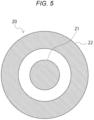
- Fig. 5 is a cross-sectional view showing a configuration example of the wave control medium 20 of a coaxial cable type according to the present embodiment.
- the wave control medium 20 according to the present embodiment is a unit structure of the metamaterial similarly to the first embodiment.
- the wave control medium 20 has a shape of a coaxial cable type.
- the wave control medium 20 is formed in, for example, a two-layer structure having a shape in which an outer surface of a coil 21, which constitutes a three-dimensional microstructure having a spiral structure similarly to the wave control medium 10 according to the first embodiment, is covered with the inner surface of a coil 22 with a minute space interposed therebetween.
- the wave control medium 20 forms a single coil structure as a whole, but has two three-dimensional microstructures including the coil 22 and the coil 21 incorporated in the coil 22.
- the wave control medium 20 is not limited to a two-layer structure and may have three or more layers, and is not limited to a single coil as a whole and may have a double or more multi-coil structure.
- the coil 21 and the coil 22 each have a shape of a thin wire.
- the coil 21 and the coil 22 form a capacitor between the outer side surface of the coil 21 and the inner side surface of the coil 22 facing each other, and form an inductor by forming a three-dimensional multiple resonance structure by the spiral structure of the coil 21 and the coil 22.
- the wave control medium 20 multiplexes the three-dimensional coil structure to increase inductance, and meanwhile, increases capacitance by acting as a capacitor in a space between the outer side surface of the coil 21 and the inner side surface of the coil 22, both of which are the thin wires. Therefore, according to the wave control medium 20, it is possible to realize a metamaterial having the broadband characteristics by being downsized with a fine structure and having the three-dimensional multiple resonance structure similarly to the first embodiment.
- Fig. 6 is a perspective view showing a configuration example of a wave control medium 30 of a double gyroid type according to the present embodiment.
- the wave control medium 30 according to the present embodiment is also a unit structure of the metamaterial similarly to the first embodiment.
- the wave control medium 30 has a shape of a double gyroid type.
- the double gyroid refers to a continuous structure in which two coils face each other and are entangled without being in contact with each other.
- the wave control medium 30 includes a coil 31 and a coil 32 of a three-dimensional microstructure, and forms a continuous three-dimensional structure in which the coil 31 and the coil 32 face each other and are entangled without being in contact with each other.
- the wave control medium 30 is not limited to a double gyroid having a double coil structure, and may be a gyroid having a multiple coil structure of three or more.
- the coil 31 and the coil 32 each have a shape of a thin wire.
- the coil 31 and the coil 32 form a capacitor between the side surface of the coil 31 and the side surface of the coil 22 facing each other, and form an inductor by forming a three-dimensional multiple resonance structure by the continuous three-dimensional structure of the coil 31 and the coil 32.
- the wave control medium 30 multiplexes the three-dimensional coil structure to increase inductance, and meanwhile, increases capacitance by acting as a capacitor in a space between the side surface of the coil 31 and the side surface of the coil 22, both of which are the thin wires. Therefore, according to the wave control medium 30, it is possible to realize a metamaterial having the broadband characteristics by being downsized with a fine structure and having the three-dimensional multiple resonance structure similarly to the first embodiment.
- Fig. 7 is a perspective view showing a configuration example of a wave control medium 40 of a cone type according to the present embodiment.
- the wave control medium 40 according to the present embodiment is also a unit structure of the metamaterial similarly to the first embodiment.
- the wave control medium 40 as a whole has a shape of a cone type extending downward in the paper surface of Fig. 7 .
- the wave control medium 40 includes a coil 41 and a coil 42 of a three-dimensional microstructure, and forms a double spiral structure of thin wires in which the coils are wound in parallel to each other while the coil 42 faces the outer side of the coil 41.
- the wave control medium 40 is not limited to a double coil, and may have a multiple coil structure of three or more.
- the wave control medium 40 as a whole has a shape of a cone type narrowing downward in the paper surface of Fig. 7 .
- the coil 41 and the coil 42 each have a shape of a thin wire.
- the coil 41 and the coil 42 form a capacitor between the side surface of the coil 41 and the side surface of the coil 42 facing each other, and form an inductor by forming a three-dimensional multiple resonance structure by the cone spiral structure of the coil 41 and the coil 42.
- the wave control medium 40 multiplexes the three-dimensional coil structure to increase inductance, and meanwhile, increases capacitance by acting as a capacitor in a space between the side surface of the coil 41 and the side surface of the coil 42, both of which are the thin wires. Therefore, according to the wave control medium 40, it is possible to realize a metamaterial having the broadband characteristics by being downsized with a fine structure and having the three-dimensional multiple resonance structure similarly to the first embodiment.
- a wave control medium is designed by a combination of a plurality of structures.
- the purpose of combining the plurality of structures is, for example, to provide a structure in which each structure functions with respect to an electric field and a magnetic field constituting an electromagnetic wave. That is, it is an object to share functions by each of the structures.
- the wave control medium can control the relative permittivity and the relative permeability to desired values with a high degree of freedom by combining a plurality of structures.
- Fig. 8 is a perspective view showing a configuration example of the wave control medium 50 according to the present embodiment.
- the wave control medium 50 is different from the wave control medium 10 according to the first embodiment in that a wire structure is combined with a double coil structure.
- Other configurations of the wave control medium 50 are similar to those of the wave control medium 10.
- the wave control medium 50 includes a coil 11 and a coil 12 which constitute a three-dimensional microstructure having a spiral structure.
- the wave control medium 50 forms a double spiral structure of thin wires in which the coils are wound in parallel to each other while the coil 12 faces the outer side of the coil 11.
- the wave control medium 50 is provided with a rod-like thin wire 51 extending in a direction in which the central axis extends at a central axis position of the spiral structure on the inner side of the coil 11.
- the wire 51 is disposed separated from the coil 11 by a minute interval.
- the coil of the wave control medium 50 is not limited to a double coil, and may be a single coil or have a multiple coil structure of three or more. In the case of multiple coils of three or more, the facing directions of the coils are not limited to be in the parallel positional relationship to each other, and it is sufficient that the coils are arranged so as not to be in direct contact with each other.
- the wire 51 has a shape of a thin wire, the wire including a material selected from any one of a metal, a dielectric, a magnetic body, a semiconductor, and a superconductor, or a combination of a plurality of these materials.
- the material of the wire 51 is not necessarily the same as that of the coil 11 and the coil 12, and the materials may be different from each other.
- the number of wires 51 is not limited to one, and may be two or more. Note that the wire 51 is not limited to a state of being contained in the coil 11 and the coil 12, and may be in a state of being adjacent to or near the coil 11 and the coil 12.
- an electric field direction of the radio wave to be applied coincides with a vibration direction of electrons in which the wire 51 extends
- a magnetic field direction of the radio wave to be applied is orthogonal to a magnetic force direction electromagnetically induced by the annular current flowing in the coil 11 and the coil 12.
- the wire 51 functions to the magnetic field
- the coil 11 and the coil 12 function to the electric field. That is, the electrons vibrating along the wire 51 function with respect to the magnetic field.
- the coil 11 and the coil 12 function with respect to the electric field.
- the wave control medium 50 can control the relative permeability and the relative permittivity to desired values with a high degree of freedom by combining a plurality of structures.
- the relative permeability and/or the relative permittivity can be finely adjusted by performing function role-sharing by combining the structure of the wire 51 to the spiral structure.
- the wave control medium 50 also serves as a capacitor between the wire 51 and the coil 11, the capacitance can be increased more than that of the wave control medium 10.
- Fig. 9 is a perspective view showing a configuration example of a wave control medium 60 as the modified example 1 of the wave control medium 50.
- the wave control medium 60 is different from the wave control medium 50 in that the wire is located outside the coil and extends in a direction orthogonal to the central axis of the coil.
- Other configurations of the wave control medium 60 are similar to those of the wave control medium 50.
- the wave control medium 60 is provided with a rod-like thin wire 61 extending in a direction orthogonal to the central axis of the spiral structure of the coil 11 and the coil 12, on the outer side of the coil 11 and the coil 12.
- the wire 61 is disposed separated from the coil 12 by a minute interval.
- the electric field direction of the radio wave to be applied coincides with the vibration direction of electrons in which the wire 61 extends
- the magnetic field direction of the radio wave to be applied coincides with the magnetic force direction electromagnetically induced by the annular current flowing in the coil 11 and the coil 12.
- the wire 61 functions to the electric field
- the coil 11 and the coil 12 function to the magnetic field. That is, the electrons vibrating along the wire 61 function with respect to the electric field.
- the magnetic force is induced at a central axis position in the center of the coil 11 and the coil 12 on the principle of electromagnetic induction, and as a result, the coil 11 and the coil 12 function with respect to the magnetic field.
- the wave control medium 60 can control the relative permittivity and the relative permeability to desired values with a high degree of freedom by combining a plurality of structures.
- the relative permittivity and/or the relative permeability can be finely adjusted by performing function role-sharing by combining the structure of the wire 61 to the spiral structure.
- Fig. 10 is a perspective view showing a configuration example of a wave control medium 70 as the modified example 2 of the wave control medium 50.
- the wave control medium 70 is different from the wave control medium 50 in that the wire is located outside the coil.
- Other configurations of the wave control medium 70 are similar to those of the wave control medium 50.
- the wave control medium 70 is provided with a rod-like thin wire 71 extending in a direction parallel to the central axis of the spiral structure of the coil 11 and the coil 12, on the outer side of the coil 11 and the coil 12.
- the wire 71 is disposed separated from the coil 12 by a minute interval.
- the electric field direction of the radio wave to be applied coincides with the vibration direction of electrons in which the wire 71 extends
- the magnetic field direction of the radio wave to be applied is orthogonal to the magnetic force direction electromagnetically induced by the annular current flowing in the coil 11 and the coil 12.
- the wire 71 functions to the magnetic field
- the coil 11 and the coil 12 function to the electric field. That is, the electrons vibrating along the wire 71 function with respect to the magnetic field.
- the coil 11 and the coil 12 function with respect to the electric field.
- the wave control medium 70 according to the present modified example can have the similar effect as the wave control medium 50.
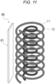
- Fig. 11 is a perspective view showing a configuration example of the wave control medium 80 according to the present embodiment.
- the wave control medium 80 is different from the wave control medium 10 according to the first embodiment in that a plate structure is combined with a double coil structure.
- Other configurations of the wave control medium 80 are similar to those of the wave control medium 10.
- the wave control medium 80 includes a coil 11 and a coil 12 similarly to the wave control medium 10. Moreover, the wave control medium 80 is provided with a thin tabular plate 81 extending in a direction parallel to the central axis of the spiral structure of the coil 11 and the coil 12, on the outer side of the coil 11 and the coil 12. The plate 81 is disposed separated from the coil 12 by a minute interval.
- the plate 81 has a shape of a thin wire, the wire including a material selected from any one of a metal, a dielectric, a magnetic body, a semiconductor, and a superconductor, or a combination of a plurality of these materials.
- the material of the plate 81 is not necessarily the same as that of the coil 11 and the coil 12, and the materials may be different from each other.
- the number of plates 81 is not limited to one, and may be two or more.
- the plate 81 can also be provided at a central axis position of the spiral structure on the inner side of the coil 11 so as to be separated from the coil 11 in a direction in which the central axis extends. In this case, because the wave control medium 80 also serves as a capacitor between the plate 81 and the coil 11, the capacitance can be increased more than that of the wave control medium 10.
- the electric field direction of the radio wave to be applied coincides with the vibration direction of electrons in which the plate 81 extends
- the magnetic field direction of the radio wave to be applied is orthogonal to the magnetic force direction electromagnetically induced by the annular current flowing in the coil 11 and the coil 12.
- the plate 81 functions to the magnetic field
- the coil 11 and the coil 12 function to the electric field. That is, the electrons vibrating along the plate 81 function with respect to the magnetic field.
- the coil 11 and the coil 12 function with respect to the electric field.
- the wave control medium 80 can control the relative permeability and the relative permittivity to desired values with a high degree of freedom by combining a plurality of structures.
- the relative permeability and/or the relative permittivity can be finely adjusted by performing function role-sharing by combining the structure of the plate 81 to the spiral structure.
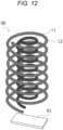
- Fig. 12 is a perspective view showing a configuration example of a wave control medium 90 as the modified example of the wave control medium 80.
- the wave control medium 90 is different from the wave control medium 80 in that the plate extends in a direction orthogonal to the central axis of the coil.
- Other configurations of the wave control medium 90 are similar to those of the wave control medium 90.
- the wave control medium 90 is provided with a tabular thin plate 91 extending in a direction orthogonal to the central axis of the spiral structure of the coil 11 and the coil 12, on the outer side of the coil 11 and the coil 12.
- the plate 91 is disposed separated from the coil 12 by a minute interval.
- the electric field direction of the radio wave to be applied coincides with the vibration direction of electrons in which the plate 91 extends
- the magnetic field direction of the radio wave to be applied coincides with the magnetic force direction electromagnetically induced by the annular current flowing in the coil 11 and the coil 12.
- the plate 91 functions to the electric field
- the coil 11 and the coil 12 function to the magnetic field. That is, the electrons vibrating along the plate 91 function with respect to the electric field.
- the magnetic force is induced at a central axis position in the center of the coil 11 and the coil 12 on the principle of electromagnetic induction, and as a result, the coil 11 and the coil 12 function with respect to the magnetic field.
- the wave control medium 90 can control the relative permittivity and the relative permeability to desired values with a high degree of freedom by combining a plurality of structures.
- the relative permittivity and/or the relative permeability can be finely adjusted by performing function role-sharing by combining the structure of the plate 81 to the spiral structure.
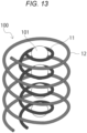
- Fig. 13 is a perspective view showing a configuration example of the wave control medium 100 according to the present embodiment.
- the wave control medium 100 is different from the wave control medium 10 according to the first embodiment in that a sphere structure is combined with a double coil structure.
- Other configurations of the wave control medium 100 are similar to those of the wave control medium 10.
- the wave control medium 100 includes a coil 11 and a coil 12 which constitute a three-dimensional microstructure similarly to the wave control medium 10. Moreover, the wave control medium 100 is provided with a plurality of spheres 101 aligned in a direction in which the central axis extends at a central axis position of the spiral structure on the inner side of the coil 11. Each of the spheres 101 is disposed separated from the coil 11 by a minute interval.
- the sphere 101 includes a material selected from any one of a metal, a dielectric, a magnetic body, a semiconductor, and a superconductor, or a combination of a plurality of these materials.
- the material of the sphere 101 is not necessarily the same as that of the coil 11 and the coil 12, and the materials may be different from each other.
- the number of the spheres 101 is not limited, and may be any number. Note that the spheres 101 can also be disposed on the outer side of the coil 11 and the coil 12.
- the electric field direction of the radio wave to be applied coincides with the vibration direction of electrons in which the spheres 101 are aligned
- the magnetic field direction of the radio wave to be applied is orthogonal to the magnetic force direction electromagnetically induced by the annular current flowing in the coil 11 and the coil 12.
- the sphere 101 functions to the magnetic field
- the coil 11 and the coil 12 function to the electric field. That is, the electrons vibrating along the sphere 101 function with respect to the magnetic field.
- the coil 11 and the coil 12 function with respect to the electric field.
- the relative permeability and/or the relative permittivity can be finely adjusted by performing function role-sharing by combining the structure of the sphere 101 to the spiral structure.
- the wave control medium 100 also serves as a capacitor between the sphere 101 and the coil 11, the capacitance can be increased more than that of the wave control medium 10.
- Fig. 14 is a cross-sectional view showing a configuration example of an electromagnetic wave absorbing member 110 according to the present embodiment perpendicular to the extending direction.
- the electromagnetic wave absorbing member (electromagnetic wave absorbing sheet) 110 has a rectangular shape in which a cross section perpendicular to the extending direction is widened in the horizontal direction.
- the electromagnetic wave absorbing member 110 includes a support 111 in a lower part and a wave control medium 112 above the support 111.
- the support 111 includes a metal, a dielectric, or a resin.
- the wave control medium 112 is a metamaterial having a resin of a wave control element in which any of the wave control media 10 to 100 described above is integrated in an array structure or a plurality of the wave control media is dispersedly disposed.
- the electromagnetic wave absorbing member 110 can absorb the irradiated electromagnetic wave by controlling a refractive index in a direction in which the electromagnetic wave is absorbed by the wave control medium 112. Furthermore, the electromagnetic wave absorbing member 110 can also be used as an electromagnetic wave shielding member for shielding the irradiated electromagnetic wave by controlling a refractive index in a direction in which the electromagnetic wave is shielded by the wave control medium 112. Moreover, the electromagnetic wave absorbing member 110 can be applied to a sensor such as an electronic toll collection system (ETC) or a radar.
- ETC electronic toll collection system
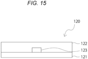
- Fig. 15 is a cross-sectional view showing a configuration example of an electromagnetic waveguide 120 according to the present embodiment perpendicular to the extending direction.
- the electromagnetic waveguide 120 has a rectangular shape in which a cross section perpendicular to the extending direction is widened in the horizontal direction.
- the electromagnetic waveguide 120 includes a support 121 at a lower part, and includes a medium 122 of silicon dioxide (SiO 2 ) or a dielectric at above the support 121.
- the support 121 includes silicon (Si), a metal, a dielectric, or a resin.
- a waveguide tube 123 having a rectangular shape with a horizontally widened cross section is provided in the central part of the medium 122 at a contact position with the support 121.
- the waveguide tube 123 includes a metamaterial having a resin of a wave control element in which any of the wave control media 10 to 100 described above is integrated in an array structure or a plurality of the wave control media is dispersedly disposed.
- the shapes of the electromagnetic waveguide 120 and the waveguide tube 123 are not limited to the present embodiment, and may be a cylindrical shape or the like.
- the electromagnetic waveguide 120 can control the refractive index of the electromagnetic wave guided to the waveguide tube 123. Furthermore, the electromagnetic waveguide 120 can be included in the arithmetic element.
- Fig. 16 is a cross-sectional view showing a configuration example of an electromagnetic waveguide 130, which is a modified example of the electromagnetic waveguide 120, perpendicular to the extending direction.
- the electromagnetic waveguide 130 is different from the electromagnetic waveguide 120 in that a layer of a material other than the wave control medium is formed in the waveguide tube.
- the overall shape of the electromagnetic waveguide 130 is similar to that of the electromagnetic waveguide 120.
- the electromagnetic waveguide 130 has a rectangular shape in which a cross section perpendicular to the extending direction is widened in the horizontal direction.
- the electromagnetic waveguide 130 includes a support 131 at a lower part, and includes a medium 132 of silicon dioxide (SiO 2 ) or a dielectric at above the support 131.
- the support 131 includes a metal, a dielectric, or a resin.
- a waveguide tube 133 having a rectangular shape with a horizontally widened cross section is provided in the central part of the medium 132 at a contact position with the support 131.
- the waveguide tube 133 includes a metamaterial having a resin of a wave control element in which any of the wave control media 10 to 100 described above is integrated in an array structure or a plurality of the wave control media is dispersedly disposed.
- a medium layer 134 including silicon (Si) or resin and having the same shape as the waveguide tube 133 is formed in the central part of the waveguide tube 133 at the contact position with the support 131.
- the electromagnetic waveguide 130 can control the refractive index of the electromagnetic wave guided to the waveguide tube 133.
- Fig. 17 is a graph for explaining an example of the specific bandwidth of the metamaterial having the wave control medium according to each of the above embodiments.
- the vertical axis represents a frequency f
- the horizontal axis represents a frequency band B.
- a curve K in Fig. 17 shows a relationship between the bandwidth B and the frequency f of the metamaterial having the wave control medium according to each of the above embodiments.
- the above specific bandwidth of the metamaterial is obtained from the curve K.
- the bandwidth refers to an inter-band distance of a frequency of 2 -1/2 of the peak frequency
- the specific bandwidth refers to a value obtained by dividing the bandwidth by the peak frequency that is the center frequency.
- the frequency is a peak frequency fc in a band Bc, and is a frequency f 1 which is 2 -1/2 of the peak frequency in the bands B 1 and B 2 . Therefore, in the curve K, the bandwidth is B 1 - B 2 , and the fractional bandwidth is (B 1 - B 2 )/fc.
- the wave control medium according to each of the above embodiments is optimum in a case where the specific bandwidth of a response is 30% or more, and the absorption intensity in the specific bandwidth is 50% or more. Therefore, according to the above embodiments, it is possible to provide a wave control element including the wave control medium according to each of the above embodiments and having a specific bandwidth of a response of 30% or more, and an absorption intensity in the specific bandwidth of 50% or more.
- the above wave control medium may be integrated in an array structure, or a plurality of the wave control media may be dispersedly disposed.
- the metamaterial having the wave control medium according to each of the above embodiments can be applied to a wave control device that performs signal transmission/reception or light reception/emission, a small antenna, a low-profile antenna, a frequency selection filter, an artificial magnetic conductor, an electro band gap member, a noise suppression member, an isolator, a radio wave lens, a radar member, an optical lens, an optical film, an optical element for terahertz, a radio wave and optical camouflage/invisibility member, a heat dissipation member, a heat shielding member, a heat storage member, a non-linear device for electromagnetic wave modulation/demodulation, wavelength conversion, and the like, a speaker, and the like.
Landscapes
- Physics & Mathematics (AREA)
- Engineering & Computer Science (AREA)
- Manufacturing & Machinery (AREA)
- Electromagnetism (AREA)
- General Physics & Mathematics (AREA)
- Optics & Photonics (AREA)
- Shielding Devices Or Components To Electric Or Magnetic Fields (AREA)
- Coils Or Transformers For Communication (AREA)
- Aerials With Secondary Devices (AREA)
- Surface Acoustic Wave Elements And Circuit Networks Thereof (AREA)
Applications Claiming Priority (2)
| Application Number | Priority Date | Filing Date | Title |
|---|---|---|---|
| JP2020196694 | 2020-11-27 | ||
| PCT/JP2021/037892 WO2022113551A1 (fr) | 2020-11-27 | 2021-10-13 | Support de commande d'onde, élément de commande d'onde, partie de commande d'onde, dispositif de commande d'onde et procédé de fabrication de support de commande d'onde |
Publications (2)
| Publication Number | Publication Date |
|---|---|
| EP4254665A1 true EP4254665A1 (fr) | 2023-10-04 |
| EP4254665A4 EP4254665A4 (fr) | 2024-06-05 |
Family
ID=81754253
Family Applications (1)
| Application Number | Title | Priority Date | Filing Date |
|---|---|---|---|
| EP21897529.0A Withdrawn EP4254665A4 (fr) | 2020-11-27 | 2021-10-13 | Support de commande d'onde, élément de commande d'onde, partie de commande d'onde, dispositif de commande d'onde et procédé de fabrication de support de commande d'onde |
Country Status (5)
| Country | Link |
|---|---|
| US (1) | US12394889B2 (fr) |
| EP (1) | EP4254665A4 (fr) |
| JP (1) | JPWO2022113551A1 (fr) |
| CN (1) | CN116508209A (fr) |
| WO (1) | WO2022113551A1 (fr) |
Families Citing this family (2)
| Publication number | Priority date | Publication date | Assignee | Title |
|---|---|---|---|---|
| US20260016712A1 (en) * | 2022-02-14 | 2026-01-15 | Sony Group Corporation | Wave control device, wavelength conversion element, arithmetic element, sensor, polarization control element, and optical isolator |
| CN115902720B (zh) * | 2022-11-01 | 2024-09-06 | 北京电磁测通科技有限公司 | 一种螺旋反射式混响室 |
Family Cites Families (6)
| Publication number | Priority date | Publication date | Assignee | Title |
|---|---|---|---|---|
| US7106918B2 (en) * | 2003-06-24 | 2006-09-12 | Massachusetts Institute Of Technology | Structurally chiral materials exhibiting magneto-gyrotropy |
| WO2010026907A1 (fr) * | 2008-09-03 | 2010-03-11 | 株式会社村田製作所 | Metamateriau |
| JP2011097334A (ja) * | 2009-10-29 | 2011-05-12 | Murata Mfg Co Ltd | アンテナ装置 |
| CN105137520B (zh) | 2015-09-22 | 2017-06-27 | 中国科学院上海技术物理研究所 | 渐变螺旋金属手性超材料圆偏振器 |
| CN106163247A (zh) * | 2016-07-18 | 2016-11-23 | 福建星宏新材料科技有限公司 | 一种宽频域吸波材料 |
| KR101894909B1 (ko) | 2016-11-15 | 2018-09-04 | 한국과학기술원 | 고굴절률 메타물질, 및 이의 제조방법 |
-
2021
- 2021-10-13 US US18/038,148 patent/US12394889B2/en active Active
- 2021-10-13 CN CN202180077488.6A patent/CN116508209A/zh active Pending
- 2021-10-13 EP EP21897529.0A patent/EP4254665A4/fr not_active Withdrawn
- 2021-10-13 JP JP2022565105A patent/JPWO2022113551A1/ja active Pending
- 2021-10-13 WO PCT/JP2021/037892 patent/WO2022113551A1/fr not_active Ceased
Also Published As
| Publication number | Publication date |
|---|---|
| US12394889B2 (en) | 2025-08-19 |
| JPWO2022113551A1 (fr) | 2022-06-02 |
| CN116508209A (zh) | 2023-07-28 |
| EP4254665A4 (fr) | 2024-06-05 |
| WO2022113551A1 (fr) | 2022-06-02 |
| US20240006749A1 (en) | 2024-01-04 |
Similar Documents
| Publication | Publication Date | Title |
|---|---|---|
| US8125717B2 (en) | Three-dimensional left-handed metamaterial | |
| JP5217494B2 (ja) | 人工媒質、その製造方法およびアンテナ装置 | |
| Alam et al. | Development of electromagnetic band gap structures in the perspective of microstrip antenna design | |
| EP2899015B1 (fr) | Matériaux indéfinis | |
| US12191569B2 (en) | Wave control medium, wave control element, wave control device, and method for manufacturing wave control medium | |
| US8860631B2 (en) | Metamaterial | |
| US12394889B2 (en) | Wave control medium, wave control element, wave control member, wave control device, and manufacturing method of wave control medium | |
| JP2021525463A (ja) | 位相制御装置、アンテナシステム及び位相制御方法 | |
| JP2003526928A (ja) | 高周波磁束のための遮蔽材 | |
| US8315500B2 (en) | Metamaterial inclusion structure and method | |
| He et al. | Ultrawide bandwidth and large-angle electromagnetic wave absorption based on triple-nested helix metamaterial absorbers | |
| EP1273068B1 (fr) | Guides pour flux magnetique h.f. | |
| CN112864615A (zh) | 一种天线和无线电设备 | |
| US8264305B2 (en) | Resonator, substrate having the same, and method of generating resonance | |
| JP6082938B2 (ja) | 3次元メタマテリアル | |
| CN108183338A (zh) | 一种皇冠型可调控的等离子体超材料宽带吸波器 | |
| JP2022130001A (ja) | 電磁波吸収体を備えたシステム、及び電磁波吸収体を用いた電磁波の吸収方法 | |
| US20260121301A1 (en) | Wave control medium, wave control element, wave control member, and wave control device | |
| KR20170004899A (ko) | 알에프 패시브 소자 및 그의 소형화 방법 | |
| CN205911398U (zh) | 同轴波导二维电磁带隙结构 | |
| Madeswaran et al. | Implementing kagome lattice photonic crystal structure for high-speed terahertz applications | |
| JP7234583B2 (ja) | 電磁波クローキング構造体 | |
| US20250227903A1 (en) | Electromagnetic wave absorber, electromagnetic wave shielding member, shielding material, electromagnetic wave absorbing sheet, sensor, device for receiving and/or transmitting, and device for receiving light and/or emitting light | |
| CN106025456A (zh) | 同轴波导二维电磁带隙结构 | |
| US11095038B2 (en) | Polarization control plate |
Legal Events
| Date | Code | Title | Description |
|---|---|---|---|
| STAA | Information on the status of an ep patent application or granted ep patent |
Free format text: STATUS: THE INTERNATIONAL PUBLICATION HAS BEEN MADE |
|
| PUAI | Public reference made under article 153(3) epc to a published international application that has entered the european phase |
Free format text: ORIGINAL CODE: 0009012 |
|
| STAA | Information on the status of an ep patent application or granted ep patent |
Free format text: STATUS: REQUEST FOR EXAMINATION WAS MADE |
|
| 17P | Request for examination filed |
Effective date: 20230606 |
|
| AK | Designated contracting states |
Kind code of ref document: A1 Designated state(s): AL AT BE BG CH CY CZ DE DK EE ES FI FR GB GR HR HU IE IS IT LI LT LU LV MC MK MT NL NO PL PT RO RS SE SI SK SM TR |
|
| DAV | Request for validation of the european patent (deleted) | ||
| DAX | Request for extension of the european patent (deleted) | ||
| A4 | Supplementary search report drawn up and despatched |
Effective date: 20240507 |
|
| RIC1 | Information provided on ipc code assigned before grant |
Ipc: H05K 9/00 20060101ALI20240430BHEP Ipc: H01Q 15/10 20060101ALI20240430BHEP Ipc: H01Q 1/36 20060101ALI20240430BHEP Ipc: G02B 1/00 20060101ALI20240430BHEP Ipc: H01Q 17/00 20060101ALI20240430BHEP Ipc: H01Q 15/14 20060101AFI20240430BHEP |
|
| STAA | Information on the status of an ep patent application or granted ep patent |
Free format text: STATUS: THE APPLICATION HAS BEEN WITHDRAWN |
|
| 18W | Application withdrawn |
Effective date: 20250221 |