EP4254720A2 - Stromversorgungsschaltung einer endgerätevorrichtung, endgerätevorrichtung und stromversorgungsverfahren - Google Patents
Stromversorgungsschaltung einer endgerätevorrichtung, endgerätevorrichtung und stromversorgungsverfahren Download PDFInfo
- Publication number
- EP4254720A2 EP4254720A2 EP23170332.3A EP23170332A EP4254720A2 EP 4254720 A2 EP4254720 A2 EP 4254720A2 EP 23170332 A EP23170332 A EP 23170332A EP 4254720 A2 EP4254720 A2 EP 4254720A2
- Authority
- EP
- European Patent Office
- Prior art keywords
- voltage
- battery
- boost circuit
- circuit
- voltage boost
- Prior art date
- Legal status (The legal status is an assumption and is not a legal conclusion. Google has not performed a legal analysis and makes no representation as to the accuracy of the status listed.)
- Granted
Links
Images




Classifications
-
- H—ELECTRICITY
- H02—GENERATION; CONVERSION OR DISTRIBUTION OF ELECTRIC POWER
- H02J—ELECTRIC POWER NETWORKS; CIRCUIT ARRANGEMENTS OR SYSTEMS FOR SUPPLYING OR DISTRIBUTING ELECTRIC POWER; SYSTEMS FOR STORING ELECTRIC ENERGY
- H02J7/00—Circuit arrangements for charging or discharging batteries or for supplying loads from batteries
- H02J7/60—Circuit arrangements for charging or discharging batteries or for supplying loads from batteries including safety or protection arrangements
- H02J7/63—Circuit arrangements for charging or discharging batteries or for supplying loads from batteries including safety or protection arrangements against overdischarge
-
- G—PHYSICS
- G05—CONTROLLING; REGULATING
- G05F—SYSTEMS FOR REGULATING ELECTRIC OR MAGNETIC VARIABLES
- G05F1/00—Automatic systems in which deviations of an electric quantity from one or more predetermined values are detected at the output of the system and fed back to a device within the system to restore the detected quantity to its predetermined value or values, i.e. retroactive systems
- G05F1/10—Regulating voltage or current
- G05F1/46—Regulating voltage or current wherein the variable actually regulated by the final control device is DC
-
- H—ELECTRICITY
- H02—GENERATION; CONVERSION OR DISTRIBUTION OF ELECTRIC POWER
- H02J—ELECTRIC POWER NETWORKS; CIRCUIT ARRANGEMENTS OR SYSTEMS FOR SUPPLYING OR DISTRIBUTING ELECTRIC POWER; SYSTEMS FOR STORING ELECTRIC ENERGY
- H02J7/00—Circuit arrangements for charging or discharging batteries or for supplying loads from batteries
- H02J7/90—Regulation of charging or discharging current or voltage
- H02J7/96—Regulation of charging or discharging current or voltage in response to battery voltage
-
- H—ELECTRICITY
- H02—GENERATION; CONVERSION OR DISTRIBUTION OF ELECTRIC POWER
- H02J—ELECTRIC POWER NETWORKS; CIRCUIT ARRANGEMENTS OR SYSTEMS FOR SUPPLYING OR DISTRIBUTING ELECTRIC POWER; SYSTEMS FOR STORING ELECTRIC ENERGY
- H02J7/00—Circuit arrangements for charging or discharging batteries or for supplying loads from batteries
-
- H—ELECTRICITY
- H02—GENERATION; CONVERSION OR DISTRIBUTION OF ELECTRIC POWER
- H02J—ELECTRIC POWER NETWORKS; CIRCUIT ARRANGEMENTS OR SYSTEMS FOR SUPPLYING OR DISTRIBUTING ELECTRIC POWER; SYSTEMS FOR STORING ELECTRIC ENERGY
- H02J7/00—Circuit arrangements for charging or discharging batteries or for supplying loads from batteries
- H02J7/40—Circuit arrangements for charging or discharging batteries or for supplying loads from batteries characterised by the exchange of charge or discharge related data
- H02J7/44—Circuit arrangements for charging or discharging batteries or for supplying loads from batteries characterised by the exchange of charge or discharge related data between battery management systems and power sources
-
- H—ELECTRICITY
- H02—GENERATION; CONVERSION OR DISTRIBUTION OF ELECTRIC POWER
- H02J—ELECTRIC POWER NETWORKS; CIRCUIT ARRANGEMENTS OR SYSTEMS FOR SUPPLYING OR DISTRIBUTING ELECTRIC POWER; SYSTEMS FOR STORING ELECTRIC ENERGY
- H02J7/00—Circuit arrangements for charging or discharging batteries or for supplying loads from batteries
- H02J7/855—Circuit arrangements for charging or discharging batteries or for supplying loads from batteries with circuits adapted for supplying loads from the battery
-
- H—ELECTRICITY
- H02—GENERATION; CONVERSION OR DISTRIBUTION OF ELECTRIC POWER
- H02J—ELECTRIC POWER NETWORKS; CIRCUIT ARRANGEMENTS OR SYSTEMS FOR SUPPLYING OR DISTRIBUTING ELECTRIC POWER; SYSTEMS FOR STORING ELECTRIC ENERGY
- H02J7/00—Circuit arrangements for charging or discharging batteries or for supplying loads from batteries
- H02J7/90—Regulation of charging or discharging current or voltage
- H02J7/96—Regulation of charging or discharging current or voltage in response to battery voltage
- H02J7/965—Regulation of charging or discharging current or voltage in response to battery voltage obtained with the battery disconnected from the charge or discharge circuit
-
- H—ELECTRICITY
- H02—GENERATION; CONVERSION OR DISTRIBUTION OF ELECTRIC POWER
- H02J—ELECTRIC POWER NETWORKS; CIRCUIT ARRANGEMENTS OR SYSTEMS FOR SUPPLYING OR DISTRIBUTING ELECTRIC POWER; SYSTEMS FOR STORING ELECTRIC ENERGY
- H02J7/00—Circuit arrangements for charging or discharging batteries or for supplying loads from batteries
- H02J7/90—Regulation of charging or discharging current or voltage
- H02J7/971—Regulation of charging or discharging current or voltage the charge cycle being controlled or terminated in response to non-electric parameters
- H02J7/975—Regulation of charging or discharging current or voltage the charge cycle being controlled or terminated in response to non-electric parameters in response to temperature
-
- H—ELECTRICITY
- H02—GENERATION; CONVERSION OR DISTRIBUTION OF ELECTRIC POWER
- H02J—ELECTRIC POWER NETWORKS; CIRCUIT ARRANGEMENTS OR SYSTEMS FOR SUPPLYING OR DISTRIBUTING ELECTRIC POWER; SYSTEMS FOR STORING ELECTRIC ENERGY
- H02J7/00—Circuit arrangements for charging or discharging batteries or for supplying loads from batteries
- H02J7/90—Regulation of charging or discharging current or voltage
- H02J7/971—Regulation of charging or discharging current or voltage the charge cycle being controlled or terminated in response to non-electric parameters
- H02J7/975—Regulation of charging or discharging current or voltage the charge cycle being controlled or terminated in response to non-electric parameters in response to temperature
- H02J7/977—Regulation of charging or discharging current or voltage the charge cycle being controlled or terminated in response to non-electric parameters in response to temperature of the battery
-
- H—ELECTRICITY
- H02—GENERATION; CONVERSION OR DISTRIBUTION OF ELECTRIC POWER
- H02M—APPARATUS FOR CONVERSION BETWEEN AC AND AC, BETWEEN AC AND DC, OR BETWEEN DC AND DC, AND FOR USE WITH MAINS OR SIMILAR POWER SUPPLY SYSTEMS; CONVERSION OF DC OR AC INPUT POWER INTO SURGE OUTPUT POWER; CONTROL OR REGULATION THEREOF
- H02M3/00—Conversion of DC power input into DC power output
- H02M3/02—Conversion of DC power input into DC power output without intermediate conversion into AC
- H02M3/04—Conversion of DC power input into DC power output without intermediate conversion into AC by static converters
- H02M3/06—Conversion of DC power input into DC power output without intermediate conversion into AC by static converters using resistors or capacitors, e.g. potential divider
- H02M3/07—Conversion of DC power input into DC power output without intermediate conversion into AC by static converters using resistors or capacitors, e.g. potential divider using capacitors charged and discharged alternately by semiconductor devices with control electrode, e.g. charge pumps
-
- H—ELECTRICITY
- H02—GENERATION; CONVERSION OR DISTRIBUTION OF ELECTRIC POWER
- H02J—ELECTRIC POWER NETWORKS; CIRCUIT ARRANGEMENTS OR SYSTEMS FOR SUPPLYING OR DISTRIBUTING ELECTRIC POWER; SYSTEMS FOR STORING ELECTRIC ENERGY
- H02J2105/00—Networks for supplying or distributing electric power characterised by their spatial reach or by the load
- H02J2105/40—Networks for supplying or distributing electric power characterised by their spatial reach or by the load characterised by the loads connecting to the networks or being supplied by the networks
- H02J2105/44—Portable electronic devices
-
- H—ELECTRICITY
- H02—GENERATION; CONVERSION OR DISTRIBUTION OF ELECTRIC POWER
- H02J—ELECTRIC POWER NETWORKS; CIRCUIT ARRANGEMENTS OR SYSTEMS FOR SUPPLYING OR DISTRIBUTING ELECTRIC POWER; SYSTEMS FOR STORING ELECTRIC ENERGY
- H02J2207/00—Details of circuit arrangements for charging or discharging batteries or supplying loads from batteries
- H02J2207/10—Control circuit supply, e.g. means for supplying power to the control circuit
-
- H—ELECTRICITY
- H02—GENERATION; CONVERSION OR DISTRIBUTION OF ELECTRIC POWER
- H02J—ELECTRIC POWER NETWORKS; CIRCUIT ARRANGEMENTS OR SYSTEMS FOR SUPPLYING OR DISTRIBUTING ELECTRIC POWER; SYSTEMS FOR STORING ELECTRIC ENERGY
- H02J2207/00—Details of circuit arrangements for charging or discharging batteries or supplying loads from batteries
- H02J2207/20—Charging or discharging characterised by the power electronics converter
-
- Y—GENERAL TAGGING OF NEW TECHNOLOGICAL DEVELOPMENTS; GENERAL TAGGING OF CROSS-SECTIONAL TECHNOLOGIES SPANNING OVER SEVERAL SECTIONS OF THE IPC; TECHNICAL SUBJECTS COVERED BY FORMER USPC CROSS-REFERENCE ART COLLECTIONS [XRACs] AND DIGESTS
- Y02—TECHNOLOGIES OR APPLICATIONS FOR MITIGATION OR ADAPTATION AGAINST CLIMATE CHANGE
- Y02E—REDUCTION OF GREENHOUSE GAS [GHG] EMISSIONS, RELATED TO ENERGY GENERATION, TRANSMISSION OR DISTRIBUTION
- Y02E60/00—Enabling technologies; Technologies with a potential or indirect contribution to GHG emissions mitigation
- Y02E60/10—Energy storage using batteries
Definitions
- This application relates to the field of terminal device technologies, and in particular, to a power supply circuit of a terminal device, a terminal device, and a power supply method.
- the terminal device needs to consume a relatively high current during photographing, an output voltage of the battery sharply drops, and severely, the terminal device is instantaneously shut down without a prompt of a low battery level. Consequently, user experience is deteriorated.
- This application provides a power supply circuit of a terminal device, a terminal device, and a power supply method, to prevent the terminal device from being abnormally shut down or restarted when an output voltage of a battery is relatively low or a temperature is relatively low.
- the invention is defined by the appended claims. Further aspects are provided to facilitate understanding the invention.
- a power supply circuit of a terminal device including a voltage boost circuit, a battery chip, and a controller.
- a battery end of the battery chip is connected to a positive electrode of a battery, and an electric energy output end of the battery chip is connected to a load.
- the battery chip is configured to provide an output voltage of the battery for the load.
- An input end of the voltage boost circuit is connected to the positive electrode of the battery, and an output end of the voltage boost circuit is connected to the load.
- the voltage boost circuit can boost an input voltage and then output a boosted voltage.
- the controller is configured to: when a sampling temperature is less than a preset temperature value and/or the output voltage of the battery is less than a first preset voltage value, control the voltage boost circuit to work and control the battery chip to stop supplying power to the load; and when an output voltage of the voltage boost circuit is less than an input voltage of the voltage boost circuit, control the battery chip and the voltage boost circuit to simultaneously supply power to the load, where the sampling temperature is a temperature of the terminal device or a temperature of the battery.
- the power supply circuit further includes a voltage comparison circuit.
- the controller is further configured to control the voltage comparison circuit to work when controlling the voltage boost circuit to work.
- the voltage comparison circuit is configured to: compare the output voltage of the voltage boost circuit with the input voltage of the voltage boost circuit; and send a trigger signal to the controller when determining that the output voltage of the voltage boost circuit is less than the input voltage of the voltage boost circuit.
- the controller is further configured to: when receiving the trigger signal, control the battery chip and the voltage boost circuit to simultaneously supply power to the load.
- the voltage comparison circuit can obtain a difference between the output voltage and the input voltage of the voltage boost circuit.
- the voltage comparison circuit may be any circuit or chip that implements the foregoing functions.
- the voltage comparison circuit may be implemented by a comparator and a peripheral building resistor. The foregoing difference is calculated by using resistors with different resistance values.
- the voltage comparison circuit sends the trigger signal to the controller only when the output voltage of the voltage boost circuit is less than the input voltage of the voltage boost circuit.
- the voltage comparison circuit sends the trigger signal to the controller only when the output voltage of the voltage boost circuit is less than the input voltage of the voltage boost circuit and the difference between the two voltages exceeds a first threshold.
- the voltage comparison circuit may be disposed inside the battery chip, or may be disposed outside the battery chip.
- the voltage comparison circuit is disposed inside the battery chip, or the voltage comparison circuit is disposed outside the battery chip.
- the battery chip includes a switch.
- a first end of the switch is connected to the battery end of the battery chip, and a second end of the switch is connected to the electric energy output end of the battery chip.
- That the controller controls the battery chip to supply power to the load is specifically: the controller controls the switch to be closed.
- the controller is further configured to: when it is detected that a charger is inserted into the terminal device, control the battery chip to supply power to the load, and control the voltage boost circuit to stop working.
- the load is directly powered by the charger.
- the controller is further configured to: after the controller controls the voltage boost circuit to work and controls the battery chip to stop supplying power to the load, when a screen of the terminal device is turned off and the output voltage of the battery is greater than a second preset voltage value, control the output voltage of the voltage boost circuit to be less than or equal to the output voltage of the battery, then control the battery chip to supply power to the load, and next control the voltage boost circuit to stop working.
- the second preset voltage value is less than the first preset voltage value.
- the voltage boost circuit may be controlled to stop working and the battery chip works to provide a power supply path for the load, provided that the output voltage of the battery is greater than the second preset voltage value.
- the controller is further configured to: after the controller controls the voltage boost circuit to stop working, when the screen of the terminal device is turned off and the output voltage of the battery is less than or equal to the second preset voltage value, control the voltage boost circuit to work and control the battery chip to stop supplying power to the load.
- the controller is further configured to control the terminal device to be shut down when the output voltage of the battery is less than or equal to a third preset voltage value.
- the third preset voltage value is less than the second preset voltage value.
- controller controls the voltage boost circuit to work and controls the battery chip to stop supplying power to the load specifically includes:
- the output voltage of the voltage boost circuit is first controlled to be less than or approximate to (for example, equal to or slightly greater than) the output voltage of the battery, then the battery chip is controlled to stop supplying power to the load, and next the output voltage of the voltage boost circuit is controlled to be a fourth preset voltage value.
- the fourth preset voltage value is less than the first preset voltage value.
- the voltage boost circuit is a boost circuit or a charge pump circuit.
- the power supply circuit further includes a power management chip.
- the power management chip is configured to: determine that the sampling temperature is less than the preset temperature value and/or the output voltage of the battery is less than the first preset voltage value; and send the determining result to the controller.
- the controller is implemented by a system-on-a-chip of the terminal device.
- the controller needs to control working states of the battery chip and the voltage boost circuit.
- the following provides a power supply circuit, so that switching between power supply paths can be automatically performed based on an output voltage of a battery without a need of control. This is simple and convenient, and further reduces control costs.
- a difference between the voltage boost circuit in the following embodiment and the voltage boost circuit in the foregoing embodiment is that a bypass circuit is added.
- a power supply circuit of a terminal device including a voltage boost circuit, a battery chip, and a controller.
- a battery end of the battery chip is connected to a positive electrode of a battery, and an electric energy output end of the battery chip is connected to a load.
- the battery chip is configured to provide an output voltage of the battery for the load.
- the voltage boost circuit has a bypass circuit. An input end of the voltage boost circuit is connected to the positive electrode of the battery, and an output end of the voltage boost circuit is connected to the load.
- the voltage boost circuit can boost an input voltage and then output a boosted voltage.
- a first end of the bypass circuit is connected to the input end of the voltage boost circuit, and a second end of the bypass circuit is connected to the output end of the voltage boost circuit.
- a conducting state of the voltage boost circuit is complementary to that of the bypass circuit.
- the controller is configured to: when a sampling temperature is less than a preset temperature value and/or the output voltage of the battery is less than a first preset voltage value, control the voltage boost circuit to work and control the battery chip to stop supplying power to the load. When an output voltage of the voltage boost circuit is less than an input voltage of the voltage boost circuit, the bypass circuit is automatically conducted to supply power to the load.
- the sampling temperature is a temperature of the terminal device or a temperature of the battery.
- the controller is further configured to: when it is detected that a charger is inserted into the terminal device, control the battery chip to supply power to the load, and control the voltage boost circuit to stop working.
- the controller is further configured to: after the controller controls the voltage boost circuit to work and controls the battery chip to stop supplying power to the load, when a screen of the terminal device is turned off and the output voltage of the battery is greater than a second preset voltage value, control the output voltage of the voltage boost circuit to be less than or equal to the output voltage of the battery, then control the battery chip to supply power to the load, and next control the voltage boost circuit to stop working.
- the second preset voltage value is less than the first preset voltage value.
- the controller is further configured to: after the controller controls the voltage boost circuit to stop working, when the screen of the terminal device is turned off and the output voltage of the battery is less than or equal to the second preset voltage value, control the voltage boost circuit to work and control the battery chip to stop supplying power to the load.
- the controller is further configured to control the terminal device to be shut down when the output voltage of the battery is less than or equal to a third preset voltage value.
- the third preset voltage value is less than the second preset voltage value.
- the controller controls the voltage boost circuit to work and controls the battery chip to stop supplying power to the load specifically includes: first controlling the output voltage of the voltage boost circuit to be less than or approximate to (for example, equal to or slightly greater than) the output voltage of the battery, then controlling the battery chip to stop supplying power to the load, and next controlling the output voltage of the voltage boost circuit to be a fourth preset voltage value.
- the fourth preset voltage value is less than the first preset voltage value.
- the voltage boost circuit is a boost circuit or a charge pump circuit.
- the power supply circuit further includes a power management chip.
- the power management chip is configured to: determine that the sampling temperature is less than the preset temperature value and/or the output voltage of the battery is less than the first preset voltage value; and send the determining result to the controller.
- the controller is implemented by a system-on-a-chip of the terminal device.
- a conducting state of the voltage boost circuit is complementary to that of the bypass circuit specifically includes: the bypass circuit is not conducted when the voltage boost circuit is conducted; or the voltage boost circuit is not conducted when the bypass circuit is conducted.
- a terminal device including a battery, a load, and the power supply circuit provided in the first aspect or the second aspect.
- the power supply circuit is configured to provide electric energy of the battery for the load.
- a power supply method for a terminal device is provided. The method is applied to the terminal device.
- the terminal device includes a battery, a load, and a power supply circuit.
- the power supply circuit includes a voltage boost circuit, a battery chip, and a controller.
- a battery end of the battery chip is connected to a positive electrode of the battery, and an electric energy output end of the battery chip is connected to the load.
- the battery chip is configured to provide an output voltage of the battery for the load.
- An input end of the voltage boost circuit is connected to the positive electrode of the battery, and an output end of the voltage boost circuit is connected to the load.
- the method includes:
- a power supply method for a terminal device is further provided.
- the method is applied to the terminal device.
- the terminal device includes a battery, a load, and a power supply circuit.
- the power supply circuit includes a voltage boost circuit, a battery chip, and a controller.
- a battery end of the battery chip is connected to a positive electrode of the battery, and an electric energy output end of the battery chip is connected to the load.
- the battery chip is configured to provide an output voltage of the battery for the load.
- An input end of the voltage boost circuit is connected to the positive electrode of the battery, and an output end of the voltage boost circuit is connected to the load.
- the voltage boost circuit has a bypass circuit. A first end of the bypass circuit is connected to the input end of the voltage boost circuit, and a second end of the bypass circuit is connected to the output end of the voltage boost circuit.
- a conducting state of the voltage boost circuit is complementary to that of the bypass circuit.
- the method includes:
- the voltage boost circuit is added to the terminal device.
- the voltage boost circuit is controlled to work.
- the output voltage of the voltage boost circuit is less than the input voltage of the voltage boost circuit, the battery chip and the voltage boost circuit are controlled to simultaneously supply power to the load.
- the sampling temperature is the temperature of the terminal device or the temperature of the battery. Therefore, according to the power supply circuit provided in the embodiments of this application, when the temperature of the terminal device is relatively low and/or the output voltage of the battery is relatively low, the output voltage of the battery may be boosted and then a boosted voltage is provided for the load.
- a power demand of the load is met, and abnormal shutdown or restart caused when the load requires a high current is avoided.
- user experience can be improved, and remaining power of the battery can be further fully used.
- a battery voltage value corresponding to shutdown of the terminal device may be further reduced, thereby prolonging a run time of the terminal device.
- the output voltage of the voltage boost circuit may be stepped down as a relatively high pulse current occurs on the load.
- the controller in this application may control both the battery chip and the voltage boost circuit to supply power to the load. In other words, two power supply paths are conducted. In this way, a power supply current can be increased, to meet a requirement of the load for a high current.
- the terminal device may be any device powered by a battery, for example, a mobile phone, a notebook computer, a wearable electronic device (such as a smartwatch), a tablet computer, an augmented reality (augmented reality, AR) device/a virtual reality (virtual reality, VR) device, or a vehicle-mounted computer device.
- a battery for example, a mobile phone, a notebook computer, a wearable electronic device (such as a smartwatch), a tablet computer, an augmented reality (augmented reality, AR) device/a virtual reality (virtual reality, VR) device, or a vehicle-mounted computer device.
- a voltage VB of a battery end drops.
- the terminal device is a mobile phone
- the VB sharply drops, and severely, the mobile phone is instantaneously shut down without a prompt of a low battery level. Consequently, user experience is deteriorated.
- internal resistance exists in the battery, and the internal resistance of the battery increases as a temperature decreases. Therefore, when an ambient temperature is relatively low or a temperature of the battery is relatively low, the internal resistance of the battery increases, and the VB drops. Consequently, the mobile phone is shut down or restarted.
- this embodiment of this application provides the power supply circuit of the terminal device.
- a voltage boost circuit is added to the terminal device.
- the voltage boost circuit is controlled to work.
- an output voltage of the voltage boost circuit is less than an input voltage of the voltage boost circuit, the battery chip and the voltage boost circuit are controlled to simultaneously supply power to the load.
- the sampling temperature is a temperature of the terminal device or a temperature of the battery.
- the power supply circuit in this embodiment of this application, when the temperature of the terminal device is relatively low and/or the output voltage of the battery is relatively low, the output voltage of the battery may be boosted and then a boosted voltage is provided for the load. In this way, a power demand of the load is met, and abnormal shutdown or restart caused when the load requires a high current is avoided.
- the output voltage of the voltage boost circuit may be stepped down as the load requires a higher current.
- the power supply circuit in this application can control both the battery chip and the voltage boost circuit to supply power to the load. In other words, two power supply paths are both conducted, and currents of the two paths are both supplied to the load. In this way, a power supply current can be increased, to meet a requirement of the load for a high current. Therefore, when the load requires a high current, the terminal device is not abnormally shut down, and can continue to be normally used, thereby further improving user experience.
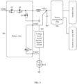
- FIG. 1 is a schematic diagram of a power supply circuit of a terminal device according to an embodiment of this application.
- the power supply circuit of the terminal device provided in this embodiment of this application includes a battery chip 100, a voltage boost circuit 300, a controller (not shown in the figure), and a power management chip 200.
- a battery end VBAT of the battery chip 100 is connected to a positive electrode of a battery BAT, and an electric energy output end VSYS of the battery chip 100 is connected to a load, for example, is connected to a system-on-a-chip SOC and another load.
- a voltage of the VBAT is denoted as VB.
- An input end of the voltage boost circuit 300 is connected to the positive electrode of the battery BAT, and an output end of the voltage boost circuit 300 is connected to the load, in other words, the output end of the voltage boost circuit 300 is connected to the electric energy output end VSYS of the battery chip 100.
- the battery chip 100 may provide an output voltage of the battery for the load.
- the battery chip 100 mainly controls charging and discharging of the battery BAT, for example, usually by using a switch-mode power supply. For example, when a charging power supply end VCHG charges the BAT, the battery chip 100 controls switchs Q1, Q2, Q3, and Q4 to be closed.
- the power management chip 200 converts electric energy of the VSYS and then supplies power to the load.
- the load includes the system-on-a-chip (SOC, System-On-a-Chip) and the another load.
- the power management chip 200 detects a value of the VS. When determining that the VS is less than a specified shutdown threshold or an under voltage lock out (UVLO, Under Voltage Lock Out) voltage, the power management chip 200 triggers the terminal device to be shut down or restarted.
- UVLO Under Voltage Lock Out
- the controller is configured to: when a sampling temperature is less than a preset temperature value and/or the output voltage of the battery is less than a first preset voltage value, control the voltage boost circuit 300 to work and control the battery chip 100 to stop supplying power to the load, to be specific, provide the output voltage of the battery for the load by using the voltage boost circuit 300; and when an output voltage of the voltage boost circuit 300 is less than an input voltage of the voltage boost circuit 300, control the battery chip 100 and the voltage boost circuit 300 to simultaneously supply power to the load.
- the sampling temperature is a temperature of the terminal device or a temperature of the battery.
- the voltage boost circuit 300 may be a circuit that can implement a voltage boost function, for example, may be a boost circuit or a charge pump circuit. It should be noted that the voltage boost circuit 300 can boost an input voltage and then provide a boosted voltage. However, the voltage boost circuit does not necessarily boost the input voltage, but only transparently transmits the input voltage. To be specific, after passing through the voltage boost circuit, the output voltage of the battery may remain unchanged, or may be boosted. For example, the output voltage of the voltage boost circuit 300 is set to V0. When the input voltage of the voltage boost circuit 300 is less than V0, the voltage boost circuit 300 boosts the input voltage to V0 and then outputs the boosted voltage. When the input voltage of the voltage boost circuit 300 is greater than V0, the voltage boost circuit 300 transparently transmits the voltage, in other words, the input voltage remains unchanged when being output by the voltage boost circuit 300.
- the sampling temperature may be obtained by a temperature sensor.
- the temperature sensor may collect the temperature of the terminal device or the temperature of the battery. For example, if the terminal device is a mobile phone, when the temperature sensor collects a temperature of the mobile phone, the temperature sensor may be disposed at any location on the mobile phone; or when the temperature sensor collects the temperature of the battery, the temperature sensor may be disposed at a location near the battery on the mobile phone.
- a relatively low temperature and a relatively low output voltage of the battery each may cause abnormal shutdown of the terminal device. Therefore, a condition for triggering the controller to control the voltage boost circuit to work may be either thereof.
- the voltage boost circuit when the temperature is relatively low, the voltage boost circuit is started to work, or when the output voltage of the battery is relatively low, the voltage boost circuit is started to work.
- the voltage boost circuit may be started only when the temperature is relatively low and the output voltage of the battery is relatively low.
- Afunction of the voltage boost circuit 300 is to boost the input voltage and then output a boosted voltage. Because the input end of the voltage boost circuit 300 is connected to the positive electrode of the battery BAT, the voltage boost circuit 300 can boost the output voltage of the battery and then output a boosted voltage to the load.
- the voltage boost circuit 300 works, if a relatively high pulse current occurs in a running process of the terminal device, the output voltage of the voltage boost circuit 300 sharply drops, to be specific, the output voltage of the voltage boost circuit 300 is less than the input voltage of the voltage boost circuit 300.
- the battery chip 100 and the voltage boost circuit 300 may be controlled to simultaneously supply power to the load, to boost a power supply current and a power supply voltage, so as to prevent the terminal device from being abnormally shut down when a relatively high pulse current occurs.
- a condition for triggering the voltage boost circuit to be started to work is that the sampling temperature is less than the preset temperature value, when the sampling temperature is greater than or equal to the preset temperature value, the voltage boost circuit does not work, and only the battery chip 100 supplies power to the load.
- Q4 when the sampling temperature is greater than or equal to the preset temperature value, Q4 is controlled to be conducted, the voltage boost circuit is controlled not to work, and only the battery chip 100 supplies power to the load.
- a condition for triggering the voltage boost circuit to be started to work is that the output voltage of the battery is less than the first preset voltage value
- the voltage boost circuit does not work, and only the battery chip 100 supplies power to the load.
- Q4 is controlled to be conducted, the voltage boost circuit is controlled not to work, and only the battery chip 100 supplies power to the load.
- a condition for triggering the voltage boost circuit to be started to work is that the sampling temperature is less than the preset temperature value and the output voltage of the battery is less than the first preset voltage value, when the sampling temperature is greater than or equal to the preset temperature value or the output voltage of the battery is greater than or equal to the first preset voltage value, the voltage boost circuit does not work, and only the battery chip 100 supplies power to the load.
- a voltage comparison circuit compares the input voltage with the output voltage of the voltage boost circuit.
- FIG. 2 is a schematic diagram of another power supply circuit of a terminal device according to an embodiment of this application.
- the power supply circuit of the terminal device provided in this embodiment includes the power supply circuit shown in FIG. 1 , and further includes a voltage comparison circuit 101.
- the controller is further configured to control the voltage comparison circuit 101 to work when controlling the voltage boost circuit 300 to work.
- the voltage comparison circuit 101 needs to work only when the voltage boost circuit 300 works.
- the voltage comparison circuit 101 is configured to: compare the output voltage of the voltage boost circuit 300 with the input voltage of the voltage boost circuit 300; and send a trigger signal to the controller when determining that the output voltage of the voltage boost circuit 300 is less than the input voltage of the voltage boost circuit 300.
- the voltage comparison circuit 101 sends a trigger signal to the controller only when the output voltage of the voltage boost circuit 300 is less than the input voltage and a difference between the two voltages exceeds a first threshold.
- the voltage comparison circuit 101 can obtain the difference between the output voltage and the input voltage of the voltage boost circuit 300.
- the voltage comparison circuit 101 may be any circuit or chip that implements the foregoing functions.
- the voltage comparison circuit 101 may be implemented by a comparator and a peripheral building resistor. The foregoing difference is calculated by using resistors with different resistance values.
- the controller is further configured to: when receiving the trigger signal sent by the voltage comparison circuit 101, control the battery chip 100 and the voltage boost circuit 300 to simultaneously supply power to the load, to be specific, control Q4 to be conducted, and control the voltage boost circuit 300 to continue to work.
- the voltage comparison circuit 101 sends the trigger signal to the controller only when the output voltage of the voltage boost circuit 300 is less than the input voltage of the voltage boost circuit 300.
- the voltage comparison circuit 101 sends the trigger signal to the controller only when the output voltage of the voltage boost circuit 300 is less than the input voltage of the voltage boost circuit 300 and the difference between the two voltages exceeds the first threshold.
- the first threshold may be set according to a requirement.
- the first threshold may be selected from 50 mV to 100 mV.
- Whether the battery chip 100 supplies power to the load may be determined by controlling a conduction/disconnection state of an internal switch inside the battery chip 100. As shown in FIG. 3 , the battery chip includes the switch Q4.
- a first end of the switch Q4 is connected to the battery end VBAT of the battery chip 100, and a second end of the switch Q4 is connected to the electric energy output end VSYS of the battery chip 100.
- That the controller controls the battery chip 100 to supply power to the load is specifically: the controller controls the switch Q4 to be closed.
- Q4 is a controllable switch.
- a conduction/disconnection state of the switch Q4 may be controlled by controlling a level of a control end of Q4.
- Q4 is conducted at a high level, and Q4 is disconnected at a low level.
- a type of Q4 is not specifically limited in this embodiment of this application.
- Q4 may be an MOS tube, an IGBT tube, or a BJT tube.
- the voltage comparison circuit 101 may be disposed inside the battery chip 100.
- the voltage comparison circuit 101 may be disposed outside the battery chip 100.
- the controller may be implemented by a system-on-a-chip SOC of the terminal device. Certainly, the controller may alternatively be disposed independently of the SOC.
- the SOC may control the voltage boost circuit 300 to work.
- the voltage boost circuit 300 has an enabling pin, and the enabling pin may be valid at a high level.
- the SOC needs to start the voltage boost circuit 300, the SOC sends a high-level signal to the enabling pin of the voltage boost circuit 300, and the voltage boost circuit 300 is started to work.
- the SOC does not send a high-level signal to the enabling pin of the voltage boost circuit 300, the enabling pin of the voltage boost circuit 300 is at a low level by default, and does not work.
- the SOC controls Q4 to be conducted, so that the battery chip 100 and the voltage boost circuit 300 simultaneously supply power to the load.
- the SOC may send a control signal to the battery chip 100, so that the battery chip 100 controls Q4 to be conducted.
- the comparison circuit 101 is disposed inside the battery chip 100, and the controller is implemented by the system-on-a-chip SOC.
- the controller is further configured to: when it is detected that a charger is inserted into the terminal device, control the battery chip 100 to supply power to the load, and control the voltage boost circuit 300 to stop working.
- the voltage boost circuit 300 may stop working, and the battery chip 100 works to provide a power supply path for the load.
- the load is directly powered by the external power supply.
- the controller controls, when determining that the sampling temperature is less than the preset temperature value and/or the output voltage of the battery is less than the first preset voltage value, the voltage boost circuit 300 to work, and controls the battery chip 100 to stop supplying power to the load, the controller is further configured to: when a screen of the terminal device is turned off and the output voltage of the battery is greater than a second preset voltage value, control the output voltage of the voltage boost circuit to be less than or equal to the output voltage of the battery, then control the battery chip to supply power to the load, and next control the voltage boost circuit to stop working.
- the second preset voltage value is less than the first preset voltage value.
- the first preset voltage value is, for example, 3.6 V
- the second preset voltage value is, for example, 3.3 V.
- the voltage boost circuit 300 may be controlled to stop working and the battery chip 100 works to provide a power supply path for the load, provided that the output voltage of the battery is greater than the second preset voltage value.
- the controller is further configured to control the voltage boost circuit to work when the screen of the terminal device is turned off and the output voltage of the battery is less than or equal to the second preset voltage value. Even if the required power decreases when the screen of the terminal device is turned off, the voltage boost circuit still needs to work when the output voltage of the battery is less than or equal to the first preset voltage value. Otherwise, the terminal device is shut down or restarted.
- controller is further configured to control the terminal device to be shut down when the output voltage of the battery is less than or equal to a third preset voltage value.
- the third preset voltage value is less than the second preset voltage value.
- the third preset voltage value is 3 Y.
- the output voltage of the battery is less than or equal to 3 V, it indicates that the battery level is very low, the battery level is insufficient to maintain normal working of the terminal device, and the terminal device needs to be shut down.
- first preset voltage value, the second preset voltage value, and the third preset voltage value in the foregoing embodiment are ranked in descending order.
- specific voltage values may be selected based on a type of the terminal device and a type of the battery. This is not specifically limited in this embodiment.
- the controller controls the voltage boost circuit to start to work and controls the battery chip to stop supplying power to the load may specifically include: first controlling the output voltage of the voltage boost circuit to be less than or equal to the output voltage of the battery, then controlling the battery chip to stop supplying power to the load, and next controlling the output voltage of the voltage boost circuit to be a fourth preset voltage value.
- the fourth preset voltage value is less than the first preset voltage value.
- the fourth preset voltage value and the second preset voltage value may be equal, for example, both are 3.3 V.
- the fourth preset voltage value and the second preset voltage value may be unequal, and may be specifically set according to an actual requirement.
- the voltage boost circuit needs to be started when the output voltage of the battery is less than the first preset voltage value.
- starting the voltage boost circuit may be understood as enabling the voltage boost circuit. If the voltage boost circuit is started only when the output voltage of the battery drops to the fourth preset voltage value, a power supply delay is caused.
- the fourth preset voltage value is usually a standard voltage required by the load, and the output voltage of the battery gradually drops as a power supply time is prolonged.
- the voltage boost circuit After the voltage boost circuit is started, if the output voltage of the battery (that is, the input voltage of the voltage boost circuit) is greater than the fourth preset voltage value, the voltage boost circuit does not boost the output voltage of the battery, but transparently transmits the output voltage of the battery. In this case, a voltage that is actually output by the voltage boost circuit is greater than the fourth preset voltage value. After the output voltage of the battery is less than the fourth preset voltage value, the voltage boost circuit boosts the output voltage of the battery to the fourth preset voltage value, and then outputs the boosted voltage. In this case, the voltage that is actually output by the voltage boost circuit is equal to the fourth preset voltage value.
- Controlling the output voltage of the voltage boost circuit to be less than the output voltage of the battery may be specifically that the output voltage of the voltage boost circuit is equal to the output voltage of the battery minus a preset threshold.
- the preset threshold may be 150 mV.
- a specific preset threshold is not specifically limited in this embodiment, and may be selected based on a type of the battery chip.
- the power supply circuit may further include a power management chip 200.
- the power management chip 200 is configured to: determine that the sampling temperature is less than the preset temperature value and/or the output voltage of the battery is less than the first preset voltage value; and send the determining result to the controller.
- the power management chip 200 determines whether the temperature is relatively low and whether the output voltage of the battery is relatively low.
- the power management chip 200 may include a direct current-direct current DC-DC conversion circuit and a low dropout regulator (LDO, Low Dropout Regulator).
- the LDO is configured to stabilize a voltage and provide the voltage for the SOC.
- LDO Low Dropout Regulator
- eMMC embedded Multi Media Card
- a circuit such as a buck-boost circuit or a boost circuit does not need to be added to an input end of the LDO, so as to reduce costs of the entire power supply circuit.
- the switching tub Q4 in the existing battery chip of the terminal device may be used to control the conduction/disconnection state of Q4 to control the power supply path of the battery chip, and the power supply path of the voltage boost circuit may be controlled by using the existing SOC of the terminal device.
- the existing SOC of the terminal device In this way, only one voltage boost circuit is added relative to a hardware facility of the existing terminal device. Therefore, costs are low, and the hardware is changed slightly, thereby facilitating popularization and application of the technical solution.
- the battery chip and the voltage boost circuit in the power supply circuit provided in this embodiment each provide a power supply path under active control.
- the switch Q4 in the battery chip 100 needs to be controlled to be closed.
- the voltage boost circuit also needs to be controlled to stop working.
- the following provides another implementation. Whether the boost voltage boosts the output voltage of the battery and then outputs a boosted voltage can be controlled.
- Q4 does not need to be controlled to be closed, but the two power supply paths are automatically conducted.
- the controller needs to control working states of the battery chip and the voltage boost circuit.
- the following provides a power supply circuit, so that switching between power supply paths can be automatically performed based on an output voltage of a battery without a need of control. This is simple and convenient, and further reduces control costs.
- a difference between a voltage boost circuit in this embodiment and the voltage boost circuit in the foregoing two embodiments lies in that a bypass circuit is added.
- FIG. 5 is a schematic diagram of yet another power supply circuit of a terminal device according to an embodiment of this application.
- the power supply circuit of the terminal device provided in this embodiment includes a voltage boost circuit 400 having a bypass circuit, a battery chip 100, and a controller.
- a battery end VBAT of the battery chip 100 is connected to a positive electrode of a battery BAT, and an electric energy output end VSYS of the battery chip 100 is connected to a load.
- the battery chip 100 is configured to provide an output voltage of the battery BAT for the load.
- the voltage boost circuit 400 having a bypass includes a voltage boost circuit and a bypass circuit.
- An input end of the voltage boost circuit is connected to the positive electrode of the battery, and an output end of the voltage boost circuit is connected to the load.
- a first end of the bypass circuit is connected to the input end of the voltage boost circuit, and a second end of the bypass circuit is connected to the output end of the voltage boost circuit.
- a conducting state of the voltage boost circuit is complementary to that of the bypass circuit.
- That a conducting state of the voltage boost circuit is complementary to that of the bypass circuit means that the bypass circuit is not conducted when the voltage boost circuit is conducted, or the voltage boost circuit is not conducted when the bypass circuit is conducted.
- a non-conducting state of the voltage boost circuit is not complementary to that of the bypass circuit. In other words, both the voltage boost circuit and the bypass circuit may be non-conducted simultaneously.
- the controller is configured to: when a sampling temperature is less than a preset temperature value and/or the output voltage of the battery is less than a first preset voltage value, control the voltage boost circuit to work and control the battery chip to stop supplying power to the load. When an output voltage of the voltage boost circuit is less than an input voltage of the voltage boost circuit, the bypass circuit is automatically conducted to supply power to the load.
- the sampling temperature is a temperature of the terminal device or a temperature of the battery.
- the voltage boost circuit works, if a relatively high pulse current occurs in a running process of the terminal device, the output voltage of the voltage boost circuit sharply drops, to be specific, the output voltage of the voltage boost circuit is less than the input voltage of the voltage boost circuit. In this case, because an input voltage of the bypass circuit is greater than an output voltage of the bypass circuit, the bypass circuit is automatically conducted, to boost a power supply current and a power supply voltage, so as to prevent the terminal device from being abnormally shut down when a relatively high pulse current occurs. The voltage boost circuit is automatically disconnected when the bypass circuit is conducted.
- the bypass circuit may be implemented by a dedicated chip.
- the chip includes both the voltage boost circuit and the bypass circuit.
- the power supply circuit may also be implemented by building the voltage boost circuit and the bypass circuit.
- the input end and the output end of the voltage boost circuit are connected to a diode in parallel.
- an anode of the diode is connected to the input end of the voltage boost circuit, and a cathode of the diode is connected to the output end of the voltage boost circuit.
- the diode is conducted.
- the voltage boost circuit is bypassed.
- the output voltage of the battery is directly output to the VSYS end through the diode, instead of passing through the voltage boost circuit.
- the voltage boost circuit works to boost the output voltage of the battery and provide a boosted voltage for the VSYS.
- the boosted voltage is greater than the output voltage of the battery. Therefore, it is equivalent to that a voltage VB of the VSYS is greater than a voltage VS of the VBAT. Therefore, the diode is reversely cut off and is not conducted.
- the output voltage of the battery does not pass through a branch in which the diode is located.
- a condition for triggering the voltage boost circuit to be started to work is that the sampling temperature is less than the preset temperature value, when the sampling temperature is greater than or equal to the preset temperature value, the voltage boost circuit does not work, and only the battery chip 100 supplies power to the load.
- a condition for triggering the voltage boost circuit to be started to work is that the output voltage of the battery is less than the first preset voltage value, when the output voltage of the battery is greater than or equal to the first preset voltage value, the voltage boost circuit does not work, and only the battery chip 100 supplies power to the load.
- a condition for triggering the voltage boost circuit to be started to work is that the sampling temperature is less than the preset temperature value and the output voltage of the battery is less than the first preset voltage value, when the sampling temperature is greater than or equal to the preset temperature value or the output voltage of the battery is greater than or equal to the first preset voltage value, the voltage boost circuit does not work, and only the battery chip 100 supplies power to the load.
- the voltage boost circuit 400 having a bypass circuit is added to the terminal device.
- the voltage boost circuit is controlled to work.
- the bypass circuit is automatically conducted to provide a power supply path for the load. Therefore, according to the power supply circuit provided in this embodiment of this application, when the temperature of the terminal device is relatively low and/or the output voltage of the battery is relatively low, the output voltage of the battery may be boosted and then a boosted voltage is provided for the load.
- the output voltage of the voltage boost circuit may be stepped down as a high pulse current occurs during power use.
- the bypass circuit is automatically conducted, to meet a requirement of the load for a high current. Therefore, when the load requires a high current, the terminal device is not abnormally shut down, and can continue to be normally used, thereby further improving user experience.
- the power management chip 200 may include a direct current-direct current DC-DC conversion circuit and a low dropout regulator (LDO, Low Dropout Regulator).
- the LDO is configured to stabilize a voltage and provide the voltage for the SOC.
- LDO Low Dropout Regulator
- eMMC embedded multimedia card
- a circuit such as a buck-boost circuit or a boost circuit does not need to be added to an input end of the LDO, so as to reduce costs of the entire power supply circuit.
- FIG. 6 is a schematic diagram of still yet another power supply circuit of a terminal device according to an embodiment of this application.
- the controller may be implemented by a system-on-a-chip SOC of the terminal device. Certainly, the controller may alternatively be disposed independently of the SOC.
- the SOC is configured to control the voltage boost circuit 400 having a bypass circuit to work.
- the voltage boost circuit 400 having a bypass circuit has an enabling pin, and the enabling pin may be valid at a high level.
- the SOC needs to start the voltage boost circuit 400 having a bypass circuit, the SOC sends a high-level signal to the enabling pin of the voltage boost circuit 400 having a bypass circuit, and the voltage boost circuit 400 having a bypass circuit is started to work.
- the SOC does not send a high-level signal to the enabling pin of the voltage boost circuit 400 having a bypass circuit
- the enabling pin of the voltage boost circuit 400 having a bypass circuit is at a low level by default, and does not work.
- the power supply circuit provided in this embodiment does not need a voltage comparison circuit. Instead, when a voltage VS of a VSYS is less than a voltage VB of a VBAT, the voltage boost circuit is conducted; otherwise, the bypass circuit is conducted.
- the voltage boost circuit 400 having a bypass circuit is enabled, conducting states of the voltage boost circuit and the bypass circuit may be automatically switched based on a voltage of an input end and a voltage of an output end without a need of control.
- the controller controls the voltage boost circuit to start to work and controls the battery chip to stop supplying power to the load may specifically include: first controlling the output voltage of the voltage boost circuit to be less than or equal to the output voltage of the battery, then controlling the battery chip to stop supplying power to the load, and next controlling the output voltage of the voltage boost circuit to be a fourth preset voltage value.
- the fourth preset voltage value is less than the first preset voltage value.
- the fourth preset voltage value and the second preset voltage value may be equal, for example, both are 3.3 V.
- the fourth preset voltage value and the second preset voltage value may be unequal, and may be specifically set according to an actual requirement.
- the voltage boost circuit needs to be started when the output voltage of the battery is less than the first preset voltage value. If the voltage boost circuit is started only when the output voltage of the battery is equal to the fourth preset voltage value, a power supply delay is caused.
- the fourth preset voltage value is usually a standard voltage required by the load, and the output voltage of the battery gradually drops as a power supply time is prolonged.
- the bypass circuit is conducted, and the voltage boost circuit does not supply power. In this case, the load is powered by the battery.
- the voltage boost circuit supplies power until the output voltage of the battery is less than the fourth preset voltage value.
- this embodiment of this application further provides a terminal device.
- the terminal device may be a mobile terminal device such as a mobile phone or an iPad, or may be another fixed terminal device that uses a battery as a power supply.
- the terminal device includes the power supply circuit provided in any one of the foregoing embodiments.
- the power supply circuit is configured to provide electric energy of the battery for a load in the terminal device.
- the voltage boost circuit When it is determined that a sampling temperature is less than a preset temperature value and/or an output voltage of the battery is less than a preset voltage value, the voltage boost circuit is controlled to work. When an output voltage of the voltage boost circuit is less than an input voltage of the voltage boost circuit, the bypass circuit is automatically conducted to provide a power supply path for the load.
- the sampling temperature is a temperature of the terminal device or a temperature of the battery. Therefore, according to the power supply circuit provided in this embodiment of this application, when the temperature of the terminal device is relatively low and/or the output voltage of the battery is relatively low, the output voltage of the battery may be boosted and then a boosted voltage is provided for the load. In this way, a power demand of the load is met, and abnormal shutdown or restart caused when the load requires a high current is avoided.
- this embodiment of this application further provides a power supply method for a terminal device.
- FIG. 7A and FIG. 7B are a flowchart of a power supply manner for a terminal device according to an embodiment of this application.
- the power supply method for the terminal device provided in this embodiment is applied to a power supply circuit.
- a power supply circuit refer to the power supply circuits shown in FIG. 1 to FIG. 4 .
- the method includes the following steps.
- a temperature of the terminal device or a temperature of the battery may be monitored in real time, and/or an output voltage of the battery may also be monitored. In this case, Q4 is closed, and the voltage boost circuit does not work.
- S802 Perform S803 when it is determined that a sampling temperature is less than a preset temperature value and/or the output voltage of the battery is less than a first preset voltage value.
- a condition for triggering the voltage boost circuit to be started to work may be determining only a temperature, or may be determining only a voltage, or may be determining both a temperature and a voltage.
- the voltage boost circuit when only the temperature is monitored, the voltage boost circuit may be started when it is determined that the temperature is less than the preset temperature value.
- the voltage boost circuit is a boost circuit, in other words, an enabling boost circuit, a chip of the boost circuit has an enabling pin.
- the voltage boost circuit when both the temperature and the voltage are determined, the voltage boost circuit may be started when it is determined that the temperature is less than the preset temperature value and it is determined that the voltage is also less than the first preset voltage value.
- the voltage may be first determined, and then the temperature is determined. An occasion for determining the voltage and the temperature is not limited in this embodiment of this application.
- the preset temperature may be set based on a specific environment in which the terminal device is located, for example, may be set to 0°C.
- the first preset voltage value may be set based on a type of the terminal device, for example, may be set to 3.6 V.
- an output voltage of the voltage boost circuit is first controlled to be less than or approximate to (for example, equal to or slightly greater than) the output voltage of the battery.
- the output voltage of the voltage boost circuit is controlled to be equal to the output voltage of the battery minus a threshold voltage.
- the threshold voltage may be selected according to a requirement, for example, may be 150 mV.
- an output voltage of the voltage boost circuit is controlled to be equal to the output voltage of the battery, then the battery chip is controlled to stop supplying power to the load, and next the output voltage of the voltage boost circuit is controlled to be a fourth preset voltage value.
- the fourth preset voltage value may be less than or equal to the first preset voltage value, and the fourth preset voltage value may be greater than or equal to a current output voltage of the battery.
- the fourth preset voltage value may alternatively be selected according to an actual requirement, for example, may be 3.3 V.
- a power supply path is provided by the voltage boost circuit for the terminal device.
- S804 Detect whether a charger is inserted into the terminal device, and if yes, perform S805.
- Control Q4 to be closed, to be specific, control the battery chip to supply power to the load, and control the voltage boost circuit to stop working.
- a power supply path is provided by the battery chip for the load of the terminal device.
- S806 Return to S801 when it is detected that the charger is removed.
- the method further includes S807.
- the method may further include S807.
- S807 Determine whether a screen of the terminal device is turned off and whether the output voltage of the battery is greater than a second preset voltage value; and if the screen is turned off and the output voltage of the battery is greater than the second preset voltage value, perform S808, or if the screen is not turned off, or if the screen is turned off but the output voltage of the battery is less than or equal to the second preset voltage value, perform S809. It should be noted that, in S807, if it is determined that the screen of the terminal device is not turned off, S809 may be directly performed without determining whether the output voltage of the battery is greater than the second preset voltage value.
- the second preset voltage value may be set according to an actual requirement, for example, may be 3.3 V.
- S808 Control the output voltage of the voltage boost circuit to be less than or equal to the output voltage of the battery, then control the battery chip to supply power to the load, in other words, close Q4, and next control the voltage boost circuit to stop working, to be specific, disable an enabling signal of the voltage boost circuit.
- a power supply path is provided by the battery chip for the terminal device.
- the power supply path may be provided by the battery chip all the time, until the terminal device is controlled to be shut down when the output voltage of the battery is less than or equal to a third preset voltage value.
- the third preset voltage value is less than the second preset voltage value.
- a power supply path may be first provided by the battery chip, and then the output voltage of the battery continues to be monitored. When the output voltage of the battery is less than the second preset voltage value, a power supply path may be provided by the voltage boost circuit, and the battery chip stops supplying power to the load.
- S809 The power supply path continues to be provided by the boost voltage for the terminal device, until the terminal device is controlled to be shut down when the output voltage of the battery is less than or equal to the third preset voltage value, where the third preset voltage value is less than the second preset voltage value.
- the third preset voltage value may be set according to an actual requirement, for example, may be 3 V. To be specific, when the output voltage of the battery is less than or equal to 3 V, the terminal device is controlled to be shut down.
- FIG. 8 is a flowchart of another power supply method for a terminal device according to an embodiment of this application.
- the power supply method for the terminal device provided in this embodiment is applied to a power supply circuit.
- a power supply circuit refer to the power supply circuits shown in FIG. 5 and FIG. 6 .
- the method includes the following steps:
- the method further includes: when it is detected that a charger is inserted into the terminal device, controlling the battery chip to supply power to the load, and controlling the voltage boost circuit to stop working.
- the output voltage of the voltage boost circuit is controlled to be less than or equal to the output voltage of the battery, then the battery chip is controlled to supply power to the load, and next the voltage boost circuit is controlled to stop working.
- the second preset voltage value is less than the first preset voltage value.
- the voltage boost circuit is controlled to work.
- the terminal device When the output voltage of the battery is less than or equal to a third preset voltage value, the terminal device is controlled to be shut down.
- the third preset voltage value is less than the second preset voltage value.
- the controlling the voltage boost circuit to work and controlling the battery chip to stop supplying power to the load may specifically include: first controlling the output voltage of the voltage boost circuit to be less than or approximate to (for example, equal to or slightly greater than) the output voltage of the battery, then controlling the battery chip to stop supplying power to the load, and next controlling the output voltage of the voltage boost circuit to be a fourth preset voltage value.
- the fourth preset voltage value is less than the first preset voltage value.
Landscapes
- Engineering & Computer Science (AREA)
- Power Engineering (AREA)
- Physics & Mathematics (AREA)
- Electromagnetism (AREA)
- General Physics & Mathematics (AREA)
- Radar, Positioning & Navigation (AREA)
- Automation & Control Theory (AREA)
- Charge And Discharge Circuits For Batteries Or The Like (AREA)
- Secondary Cells (AREA)
- Power Sources (AREA)
Priority Applications (1)
| Application Number | Priority Date | Filing Date | Title |
|---|---|---|---|
| EP23170332.3A EP4254720B1 (de) | 2018-07-27 | 2018-07-27 | Stromversorgungsschaltung einer endgerätevorrichtung, endgerätevorrichtung und stromversorgungsverfahren |
Applications Claiming Priority (3)
| Application Number | Priority Date | Filing Date | Title |
|---|---|---|---|
| EP23170332.3A EP4254720B1 (de) | 2018-07-27 | 2018-07-27 | Stromversorgungsschaltung einer endgerätevorrichtung, endgerätevorrichtung und stromversorgungsverfahren |
| EP18928090.2A EP3800760B1 (de) | 2018-07-27 | 2018-07-27 | Stromversorgungsschaltung einer endgerätevorrichtung, endgerätevorrichtung und stromversorgungsverfahren |
| PCT/CN2018/097431 WO2020019300A1 (zh) | 2018-07-27 | 2018-07-27 | 一种终端设备的供电电路、终端设备及供电方法 |
Related Parent Applications (2)
| Application Number | Title | Priority Date | Filing Date |
|---|---|---|---|
| EP18928090.2A Division EP3800760B1 (de) | 2018-07-27 | 2018-07-27 | Stromversorgungsschaltung einer endgerätevorrichtung, endgerätevorrichtung und stromversorgungsverfahren |
| EP18928090.2A Division-Into EP3800760B1 (de) | 2018-07-27 | 2018-07-27 | Stromversorgungsschaltung einer endgerätevorrichtung, endgerätevorrichtung und stromversorgungsverfahren |
Publications (3)
| Publication Number | Publication Date |
|---|---|
| EP4254720A2 true EP4254720A2 (de) | 2023-10-04 |
| EP4254720A3 EP4254720A3 (de) | 2023-11-15 |
| EP4254720B1 EP4254720B1 (de) | 2024-10-23 |
Family
ID=69181170
Family Applications (2)
| Application Number | Title | Priority Date | Filing Date |
|---|---|---|---|
| EP18928090.2A Active EP3800760B1 (de) | 2018-07-27 | 2018-07-27 | Stromversorgungsschaltung einer endgerätevorrichtung, endgerätevorrichtung und stromversorgungsverfahren |
| EP23170332.3A Active EP4254720B1 (de) | 2018-07-27 | 2018-07-27 | Stromversorgungsschaltung einer endgerätevorrichtung, endgerätevorrichtung und stromversorgungsverfahren |
Family Applications Before (1)
| Application Number | Title | Priority Date | Filing Date |
|---|---|---|---|
| EP18928090.2A Active EP3800760B1 (de) | 2018-07-27 | 2018-07-27 | Stromversorgungsschaltung einer endgerätevorrichtung, endgerätevorrichtung und stromversorgungsverfahren |
Country Status (6)
| Country | Link |
|---|---|
| US (1) | US11949272B2 (de) |
| EP (2) | EP3800760B1 (de) |
| JP (1) | JP7169444B2 (de) |
| CN (3) | CN115632454B (de) |
| RU (1) | RU2757198C1 (de) |
| WO (1) | WO2020019300A1 (de) |
Families Citing this family (21)
| Publication number | Priority date | Publication date | Assignee | Title |
|---|---|---|---|---|
| US11652315B2 (en) * | 2018-04-17 | 2023-05-16 | Aptiv Technologies Limited | Electrical power supply device |
| CN115632454B (zh) * | 2018-07-27 | 2023-10-13 | 荣耀终端有限公司 | 一种终端设备的供电电路、终端设备及供电方法 |
| JP2021122866A (ja) * | 2020-01-31 | 2021-08-30 | セイコーエプソン株式会社 | ロボット、ロボット搭載用移動体および移動ロボット |
| CN114518796B (zh) * | 2020-11-20 | 2024-12-10 | 神讯电脑(昆山)有限公司 | 双向保护电路及具有双向保护电路的电子装置 |
| US20240250542A1 (en) * | 2021-05-08 | 2024-07-25 | Harman International Industries, Incorporated | Charging device for wearable device and wearable device assembly |
| CN113448419B (zh) * | 2021-05-22 | 2023-02-28 | 山东英信计算机技术有限公司 | 一种延长服务器掉电的系统和服务器 |
| CN115693815A (zh) * | 2021-07-29 | 2023-02-03 | 北京小米移动软件有限公司 | 供电模组、终端设备、供电方法及装置 |
| CN113765177B (zh) * | 2021-07-30 | 2024-06-11 | 华为数字能源技术有限公司 | 一种电池模块和充电系统 |
| CN113937856B (zh) * | 2021-10-16 | 2023-03-24 | 深圳市海曼科技股份有限公司 | 防止电池供电设备中单片机因降压而复位的系统及方法 |
| TWI805407B (zh) * | 2022-01-12 | 2023-06-11 | 立錡科技股份有限公司 | 能減弱振鈴的升降壓切換式電源電路及其控制方法 |
| CN116667468B (zh) * | 2022-02-17 | 2023-12-26 | 荣耀终端有限公司 | 电子设备 |
| CN115001065B (zh) * | 2022-04-06 | 2026-01-27 | 华为技术有限公司 | 一种电路、供电方法、电子设备及计算机程序产品 |
| CN114865804B (zh) | 2022-04-12 | 2023-06-06 | 荣耀终端有限公司 | 一种电子设备及智能功率放大器的供电方法 |
| CN116054300B (zh) * | 2022-06-27 | 2023-10-20 | 荣耀终端有限公司 | 终端的供电电路、供电方法和终端 |
| CN115208009B (zh) * | 2022-07-07 | 2024-04-30 | 深圳拓邦股份有限公司 | 电池保护电路及电器 |
| CN116320113A (zh) * | 2023-03-16 | 2023-06-23 | 维沃移动通信有限公司 | 电子设备 |
| CN116634541B (zh) * | 2023-07-19 | 2023-11-07 | 荣耀终端有限公司 | 一种供电电路、供电方法和电子设备 |
| US12512757B2 (en) * | 2024-02-12 | 2025-12-30 | Qualcomm Incorporated | Power supply circuit with power supply rails independently monitored for load attacks |
| CN117879116B (zh) * | 2024-03-11 | 2024-05-17 | 深圳市积加创新技术有限公司 | 一种基于电池电压调整输出驱动系统及方法 |
| CN121584839A (zh) * | 2024-08-12 | 2026-02-27 | 荣耀终端股份有限公司 | 一种供电系统及电子设备 |
| CN119182204A (zh) * | 2024-11-22 | 2024-12-24 | 鼎道智芯(上海)半导体有限公司 | 充放电控制电路、方法、电源管理芯片及电子设备 |
Family Cites Families (32)
| Publication number | Priority date | Publication date | Assignee | Title |
|---|---|---|---|---|
| US6167289A (en) | 1998-02-20 | 2000-12-26 | Qualcomm Incorporated | Power supply assembly for portable phone |
| JP2003189485A (ja) | 2001-12-11 | 2003-07-04 | Sanyo Electric Co Ltd | 携帯機器 |
| JP2004312867A (ja) | 2003-04-07 | 2004-11-04 | Nec Tokin Corp | 電池用電源回路および電池パック |
| WO2005013455A1 (en) * | 2003-08-05 | 2005-02-10 | Matsushita Electric Industrial Co., Ltd. | Direct-current power supply and battery-powered electronic apparatus equipped with the power supply |
| DE102004036814B4 (de) * | 2004-07-29 | 2006-06-01 | Siemens Ag | Vorrichtung zur Versorgung einer Kraftstoffpumpe einer Brennkraftmaschine eines Kraftfahrzeuges mit elektrischem Strom |
| JP2006081369A (ja) * | 2004-09-13 | 2006-03-23 | Casio Comput Co Ltd | 電子機器 |
| US20060119322A1 (en) * | 2004-12-04 | 2006-06-08 | Hossein Maleki | Battery pack with temperature activated boost |
| WO2008030398A2 (en) | 2006-09-05 | 2008-03-13 | Summit Microelectronics, Inc | Circuits and methods for controlling power in a battery operated system |
| TW200950296A (en) * | 2008-05-20 | 2009-12-01 | Acbel Polytech Inc | Switched power supply capable of raising light-load efficiency |
| US9240883B2 (en) | 2008-09-04 | 2016-01-19 | Intel Corporation | Multi-key cryptography for encrypting file system acceleration |
| CN201349211Y (zh) | 2008-12-16 | 2009-11-18 | 宇龙计算机通信科技(深圳)有限公司 | 一种移动终端的供电系统及移动终端 |
| JP2010239832A (ja) * | 2009-03-31 | 2010-10-21 | Panasonic Corp | 電流制限回路 |
| BRPI1010083A2 (pt) | 2009-06-22 | 2016-03-15 | Koninkl Philips Electronics Nv | unidade de alimetação para alimentar um dispositivo operado eletricamente com energia elétrica e/ou sinal elétrico por meio de elementos conectores para um contato liberável de meios conectoresdedicados do dispositivo operado eletricamente, dispositivo operado eletricamente para cooperar com a unidade de alimentação, sistema elétrico e método para alimentar um dispositivo operado eletricamente com energia elétrica e/ou sinal elétrico por meio de elementos conctores para um contato liberável de meios conectores dedicados do dispositivo operado eletricamente |
| KR101097262B1 (ko) * | 2009-12-28 | 2011-12-21 | 삼성에스디아이 주식회사 | 배터리 팩, 이의 충전방법 |
| KR101745418B1 (ko) | 2010-12-30 | 2017-06-12 | 엘지디스플레이 주식회사 | 전원 공급부 및 이를 포함하는 액정표시장치 |
| CN102496042A (zh) * | 2011-12-21 | 2012-06-13 | 天龙智联(北京)科技有限公司 | 一种电子标签设备 |
| KR101923585B1 (ko) * | 2012-07-11 | 2018-11-30 | 삼성전자 주식회사 | 휴대단말기의 전원공급장치 및 방법 |
| CN103181054B (zh) * | 2012-08-07 | 2015-11-25 | 华为终端有限公司 | 用于供电的装置、方法和用户设备 |
| CN103872715A (zh) * | 2012-12-14 | 2014-06-18 | 鸿富锦精密工业(深圳)有限公司 | 手持设备及其电源电路 |
| JP6196466B2 (ja) | 2013-05-10 | 2017-09-13 | Fdk株式会社 | 電源装置 |
| JP6152241B2 (ja) * | 2014-04-23 | 2017-06-21 | レノボ・シンガポール・プライベート・リミテッド | 電力システム、携帯式電子機器および電力の供給方法 |
| CN104009529B (zh) | 2014-06-13 | 2016-08-24 | 南京矽力杰半导体技术有限公司 | 控制电路、电池供电装置和控制方法 |
| CN115498743A (zh) | 2015-03-13 | 2022-12-20 | 苏州宝时得电动工具有限公司 | 电能提供装置 |
| CN106299548A (zh) | 2015-05-28 | 2017-01-04 | 西安中兴新软件有限责任公司 | 一种温度控制方法及装置 |
| CN204886326U (zh) | 2015-08-27 | 2015-12-16 | 广东小天才科技有限公司 | 一种提高电池可用容量电路 |
| CN105337374A (zh) | 2015-12-04 | 2016-02-17 | 上海斐讯数据通信技术有限公司 | 一种提高供电时间的方法 |
| CN107783580A (zh) | 2016-08-26 | 2018-03-09 | 中兴通讯股份有限公司 | 一种电源供电控制电路及采用控制电路进行供电的方法 |
| CN108267972B (zh) | 2016-12-30 | 2021-08-03 | 北京小米移动软件有限公司 | 电子设备控制方法和装置 |
| CN107359654A (zh) * | 2017-06-01 | 2017-11-17 | 金卡智能集团股份有限公司 | 一种计量仪表无线通信装置电源控制系统 |
| CN207098681U (zh) | 2017-07-24 | 2018-03-13 | 杭州萤石网络有限公司 | 一种锂电池充放电保护电路 |
| CN108258904A (zh) * | 2017-12-01 | 2018-07-06 | 珠海格力电器股份有限公司 | 直流电源及其供电方法 |
| CN115632454B (zh) | 2018-07-27 | 2023-10-13 | 荣耀终端有限公司 | 一种终端设备的供电电路、终端设备及供电方法 |
-
2018
- 2018-07-27 CN CN202211267625.5A patent/CN115632454B/zh active Active
- 2018-07-27 CN CN202211284671.6A patent/CN115833298B/zh active Active
- 2018-07-27 WO PCT/CN2018/097431 patent/WO2020019300A1/zh not_active Ceased
- 2018-07-27 US US17/259,045 patent/US11949272B2/en active Active
- 2018-07-27 RU RU2021103291A patent/RU2757198C1/ru active
- 2018-07-27 EP EP18928090.2A patent/EP3800760B1/de active Active
- 2018-07-27 EP EP23170332.3A patent/EP4254720B1/de active Active
- 2018-07-27 CN CN201880071372.XA patent/CN111316528B/zh active Active
- 2018-07-27 JP JP2021524083A patent/JP7169444B2/ja active Active
Also Published As
| Publication number | Publication date |
|---|---|
| US11949272B2 (en) | 2024-04-02 |
| EP4254720A3 (de) | 2023-11-15 |
| EP3800760A4 (de) | 2021-12-01 |
| EP4254720B1 (de) | 2024-10-23 |
| CN111316528A (zh) | 2020-06-19 |
| JP7169444B2 (ja) | 2022-11-10 |
| CN115632454A (zh) | 2023-01-20 |
| JP2021532724A (ja) | 2021-11-25 |
| RU2757198C1 (ru) | 2021-10-12 |
| CN115833298B (zh) | 2023-08-22 |
| EP3800760A1 (de) | 2021-04-07 |
| WO2020019300A1 (zh) | 2020-01-30 |
| EP3800760B1 (de) | 2023-06-28 |
| CN115632454B (zh) | 2023-10-13 |
| CN111316528B (zh) | 2022-11-01 |
| US20210273475A1 (en) | 2021-09-02 |
| CN115833298A (zh) | 2023-03-21 |
Similar Documents
| Publication | Publication Date | Title |
|---|---|---|
| EP3800760B1 (de) | Stromversorgungsschaltung einer endgerätevorrichtung, endgerätevorrichtung und stromversorgungsverfahren | |
| US11050279B2 (en) | Charge/discharge switch control circuits for batteries | |
| US9502917B2 (en) | Charging method of electronic cigarettes and electronic cigarette box | |
| US9825478B2 (en) | Method for supplying power to a load within a portable electronic device | |
| US8860373B2 (en) | Protective circuit and charging device | |
| US20120187897A1 (en) | Battery charger for use with low voltage energy harvesting device | |
| US20170244261A1 (en) | Power bank with charging management | |
| EP3007306A1 (de) | Ladeverfahren für eine elektronische zigarette und schachtel für elektronische zigaretten | |
| US10277052B2 (en) | Controlling power delivery to a battery | |
| US12531425B2 (en) | Circuit, power supply method, electronic device, and computer program product | |
| CN106249830B (zh) | 电能传输系统及方法 | |
| CN112119563A (zh) | 蓄电系统 | |
| CN112531814A (zh) | 一种多电池充电管理系统及方法 | |
| CN217467616U (zh) | 电源控制电路和电子设备 | |
| CN103532212A (zh) | 一种充电管理电路及移动电源 | |
| CN112821546B (zh) | 多电池不间断供电装置、x-射线成像系统、供电控制方法 | |
| CN222775985U (zh) | 终端设备 | |
| US20040177282A1 (en) | Method and circuit for controlling battery charge and supply by microprocessor | |
| CN111030237B (zh) | 移动电源及其工作方法 | |
| US20250082026A1 (en) | Power-supply mode switching circuit and aerosol generating device | |
| CN113555916B (zh) | 充电电路 | |
| WO2026066454A1 (zh) | 低压配电集成架构、配电系统以及车辆 | |
| CN120855565A (zh) | 一种双电池供电系统及其双电池供电电路、供电切换方法 |
Legal Events
| Date | Code | Title | Description |
|---|---|---|---|
| PUAI | Public reference made under article 153(3) epc to a published international application that has entered the european phase |
Free format text: ORIGINAL CODE: 0009012 |
|
| STAA | Information on the status of an ep patent application or granted ep patent |
Free format text: STATUS: REQUEST FOR EXAMINATION WAS MADE |
|
| 17P | Request for examination filed |
Effective date: 20230427 |
|
| AC | Divisional application: reference to earlier application |
Ref document number: 3800760 Country of ref document: EP Kind code of ref document: P |
|
| AK | Designated contracting states |
Kind code of ref document: A2 Designated state(s): AL AT BE BG CH CY CZ DE DK EE ES FI FR GB GR HR HU IE IS IT LI LT LU LV MC MK MT NL NO PL PT RO RS SE SI SK SM TR |
|
| PUAL | Search report despatched |
Free format text: ORIGINAL CODE: 0009013 |
|
| AK | Designated contracting states |
Kind code of ref document: A3 Designated state(s): AL AT BE BG CH CY CZ DE DK EE ES FI FR GB GR HR HU IE IS IT LI LT LU LV MC MK MT NL NO PL PT RO RS SE SI SK SM TR |
|
| RIC1 | Information provided on ipc code assigned before grant |
Ipc: H02J 7/00 20060101AFI20231011BHEP |
|
| GRAP | Despatch of communication of intention to grant a patent |
Free format text: ORIGINAL CODE: EPIDOSNIGR1 |
|
| STAA | Information on the status of an ep patent application or granted ep patent |
Free format text: STATUS: GRANT OF PATENT IS INTENDED |
|
| INTG | Intention to grant announced |
Effective date: 20240521 |
|
| GRAS | Grant fee paid |
Free format text: ORIGINAL CODE: EPIDOSNIGR3 |
|
| GRAA | (expected) grant |
Free format text: ORIGINAL CODE: 0009210 |
|
| STAA | Information on the status of an ep patent application or granted ep patent |
Free format text: STATUS: THE PATENT HAS BEEN GRANTED |
|
| AC | Divisional application: reference to earlier application |
Ref document number: 3800760 Country of ref document: EP Kind code of ref document: P |
|
| AK | Designated contracting states |
Kind code of ref document: B1 Designated state(s): AL AT BE BG CH CY CZ DE DK EE ES FI FR GB GR HR HU IE IS IT LI LT LU LV MC MK MT NL NO PL PT RO RS SE SI SK SM TR |
|
| REG | Reference to a national code |
Ref country code: GB Ref legal event code: FG4D |
|
| REG | Reference to a national code |
Ref country code: CH Ref legal event code: EP |
|
| REG | Reference to a national code |
Ref country code: DE Ref legal event code: R096 Ref document number: 602018075893 Country of ref document: DE |
|
| REG | Reference to a national code |
Ref country code: IE Ref legal event code: FG4D |
|
| REG | Reference to a national code |
Ref country code: NL Ref legal event code: FP |
|
| REG | Reference to a national code |
Ref country code: LT Ref legal event code: MG9D |
|
| REG | Reference to a national code |
Ref country code: AT Ref legal event code: MK05 Ref document number: 1735646 Country of ref document: AT Kind code of ref document: T Effective date: 20241023 |
|
| PG25 | Lapsed in a contracting state [announced via postgrant information from national office to epo] |
Ref country code: PT Free format text: LAPSE BECAUSE OF FAILURE TO SUBMIT A TRANSLATION OF THE DESCRIPTION OR TO PAY THE FEE WITHIN THE PRESCRIBED TIME-LIMIT Effective date: 20250224 Ref country code: IS Free format text: LAPSE BECAUSE OF FAILURE TO SUBMIT A TRANSLATION OF THE DESCRIPTION OR TO PAY THE FEE WITHIN THE PRESCRIBED TIME-LIMIT Effective date: 20250223 Ref country code: HR Free format text: LAPSE BECAUSE OF FAILURE TO SUBMIT A TRANSLATION OF THE DESCRIPTION OR TO PAY THE FEE WITHIN THE PRESCRIBED TIME-LIMIT Effective date: 20241023 |
|
| PG25 | Lapsed in a contracting state [announced via postgrant information from national office to epo] |
Ref country code: FI Free format text: LAPSE BECAUSE OF FAILURE TO SUBMIT A TRANSLATION OF THE DESCRIPTION OR TO PAY THE FEE WITHIN THE PRESCRIBED TIME-LIMIT Effective date: 20241023 |
|
| PG25 | Lapsed in a contracting state [announced via postgrant information from national office to epo] |
Ref country code: BG Free format text: LAPSE BECAUSE OF FAILURE TO SUBMIT A TRANSLATION OF THE DESCRIPTION OR TO PAY THE FEE WITHIN THE PRESCRIBED TIME-LIMIT Effective date: 20241023 |
|
| PG25 | Lapsed in a contracting state [announced via postgrant information from national office to epo] |
Ref country code: ES Free format text: LAPSE BECAUSE OF FAILURE TO SUBMIT A TRANSLATION OF THE DESCRIPTION OR TO PAY THE FEE WITHIN THE PRESCRIBED TIME-LIMIT Effective date: 20241023 |
|
| PG25 | Lapsed in a contracting state [announced via postgrant information from national office to epo] |
Ref country code: NO Free format text: LAPSE BECAUSE OF FAILURE TO SUBMIT A TRANSLATION OF THE DESCRIPTION OR TO PAY THE FEE WITHIN THE PRESCRIBED TIME-LIMIT Effective date: 20250123 |
|
| PG25 | Lapsed in a contracting state [announced via postgrant information from national office to epo] |
Ref country code: LV Free format text: LAPSE BECAUSE OF FAILURE TO SUBMIT A TRANSLATION OF THE DESCRIPTION OR TO PAY THE FEE WITHIN THE PRESCRIBED TIME-LIMIT Effective date: 20241023 Ref country code: AT Free format text: LAPSE BECAUSE OF FAILURE TO SUBMIT A TRANSLATION OF THE DESCRIPTION OR TO PAY THE FEE WITHIN THE PRESCRIBED TIME-LIMIT Effective date: 20241023 Ref country code: GR Free format text: LAPSE BECAUSE OF FAILURE TO SUBMIT A TRANSLATION OF THE DESCRIPTION OR TO PAY THE FEE WITHIN THE PRESCRIBED TIME-LIMIT Effective date: 20250124 |
|
| PG25 | Lapsed in a contracting state [announced via postgrant information from national office to epo] |
Ref country code: PL Free format text: LAPSE BECAUSE OF FAILURE TO SUBMIT A TRANSLATION OF THE DESCRIPTION OR TO PAY THE FEE WITHIN THE PRESCRIBED TIME-LIMIT Effective date: 20241023 |
|
| PG25 | Lapsed in a contracting state [announced via postgrant information from national office to epo] |
Ref country code: RS Free format text: LAPSE BECAUSE OF FAILURE TO SUBMIT A TRANSLATION OF THE DESCRIPTION OR TO PAY THE FEE WITHIN THE PRESCRIBED TIME-LIMIT Effective date: 20250123 |
|
| PG25 | Lapsed in a contracting state [announced via postgrant information from national office to epo] |
Ref country code: SM Free format text: LAPSE BECAUSE OF FAILURE TO SUBMIT A TRANSLATION OF THE DESCRIPTION OR TO PAY THE FEE WITHIN THE PRESCRIBED TIME-LIMIT Effective date: 20241023 |
|
| PG25 | Lapsed in a contracting state [announced via postgrant information from national office to epo] |
Ref country code: DK Free format text: LAPSE BECAUSE OF FAILURE TO SUBMIT A TRANSLATION OF THE DESCRIPTION OR TO PAY THE FEE WITHIN THE PRESCRIBED TIME-LIMIT Effective date: 20241023 |
|
| PGFP | Annual fee paid to national office [announced via postgrant information from national office to epo] |
Ref country code: GB Payment date: 20250605 Year of fee payment: 8 |
|
| PGFP | Annual fee paid to national office [announced via postgrant information from national office to epo] |
Ref country code: NL Payment date: 20250613 Year of fee payment: 8 |
|
| PG25 | Lapsed in a contracting state [announced via postgrant information from national office to epo] |
Ref country code: EE Free format text: LAPSE BECAUSE OF FAILURE TO SUBMIT A TRANSLATION OF THE DESCRIPTION OR TO PAY THE FEE WITHIN THE PRESCRIBED TIME-LIMIT Effective date: 20241023 |
|
| PG25 | Lapsed in a contracting state [announced via postgrant information from national office to epo] |
Ref country code: RO Free format text: LAPSE BECAUSE OF FAILURE TO SUBMIT A TRANSLATION OF THE DESCRIPTION OR TO PAY THE FEE WITHIN THE PRESCRIBED TIME-LIMIT Effective date: 20241023 |
|
| REG | Reference to a national code |
Ref country code: DE Ref legal event code: R097 Ref document number: 602018075893 Country of ref document: DE |
|
| PG25 | Lapsed in a contracting state [announced via postgrant information from national office to epo] |
Ref country code: SK Free format text: LAPSE BECAUSE OF FAILURE TO SUBMIT A TRANSLATION OF THE DESCRIPTION OR TO PAY THE FEE WITHIN THE PRESCRIBED TIME-LIMIT Effective date: 20241023 |
|
| PG25 | Lapsed in a contracting state [announced via postgrant information from national office to epo] |
Ref country code: CZ Free format text: LAPSE BECAUSE OF FAILURE TO SUBMIT A TRANSLATION OF THE DESCRIPTION OR TO PAY THE FEE WITHIN THE PRESCRIBED TIME-LIMIT Effective date: 20241023 |
|
| PG25 | Lapsed in a contracting state [announced via postgrant information from national office to epo] |
Ref country code: IT Free format text: LAPSE BECAUSE OF FAILURE TO SUBMIT A TRANSLATION OF THE DESCRIPTION OR TO PAY THE FEE WITHIN THE PRESCRIBED TIME-LIMIT Effective date: 20241023 |
|
| PLBE | No opposition filed within time limit |
Free format text: ORIGINAL CODE: 0009261 |
|
| STAA | Information on the status of an ep patent application or granted ep patent |
Free format text: STATUS: NO OPPOSITION FILED WITHIN TIME LIMIT |
|
| PG25 | Lapsed in a contracting state [announced via postgrant information from national office to epo] |
Ref country code: SE Free format text: LAPSE BECAUSE OF FAILURE TO SUBMIT A TRANSLATION OF THE DESCRIPTION OR TO PAY THE FEE WITHIN THE PRESCRIBED TIME-LIMIT Effective date: 20241023 |
|
| 26N | No opposition filed |
Effective date: 20250724 |
|
| PGFP | Annual fee paid to national office [announced via postgrant information from national office to epo] |
Ref country code: DE Payment date: 20250604 Year of fee payment: 8 |
|
| REG | Reference to a national code |
Ref country code: CH Ref legal event code: H13 Free format text: ST27 STATUS EVENT CODE: U-0-0-H10-H13 (AS PROVIDED BY THE NATIONAL OFFICE) Effective date: 20260224 |
|
| PG25 | Lapsed in a contracting state [announced via postgrant information from national office to epo] |
Ref country code: LU Free format text: LAPSE BECAUSE OF NON-PAYMENT OF DUE FEES Effective date: 20250727 |
|
| REG | Reference to a national code |
Ref country code: BE Ref legal event code: MM Effective date: 20250731 |
|
| PG25 | Lapsed in a contracting state [announced via postgrant information from national office to epo] |
Ref country code: BE Free format text: LAPSE BECAUSE OF NON-PAYMENT OF DUE FEES Effective date: 20250731 |
|
| PG25 | Lapsed in a contracting state [announced via postgrant information from national office to epo] |
Ref country code: FR Free format text: LAPSE BECAUSE OF NON-PAYMENT OF DUE FEES Effective date: 20250731 |
|
| PG25 | Lapsed in a contracting state [announced via postgrant information from national office to epo] |
Ref country code: CH Free format text: LAPSE BECAUSE OF NON-PAYMENT OF DUE FEES Effective date: 20250731 |