EP4258047A2 - Prétraitement de couches minces d'oxyde conducteur transparent (oct) pour améliorer le contact électrique - Google Patents
Prétraitement de couches minces d'oxyde conducteur transparent (oct) pour améliorer le contact électrique Download PDFInfo
- Publication number
- EP4258047A2 EP4258047A2 EP23188618.5A EP23188618A EP4258047A2 EP 4258047 A2 EP4258047 A2 EP 4258047A2 EP 23188618 A EP23188618 A EP 23188618A EP 4258047 A2 EP4258047 A2 EP 4258047A2
- Authority
- EP
- European Patent Office
- Prior art keywords
- layer
- sub
- optical device
- electrochromic
- oxide
- Prior art date
- Legal status (The legal status is an assumption and is not a legal conclusion. Google has not performed a legal analysis and makes no representation as to the accuracy of the status listed.)
- Pending
Links
Images

Classifications
-
- G—PHYSICS
- G02—OPTICS
- G02F—OPTICAL DEVICES OR ARRANGEMENTS FOR THE CONTROL OF LIGHT BY MODIFICATION OF THE OPTICAL PROPERTIES OF THE MEDIA OF THE ELEMENTS INVOLVED THEREIN; NON-LINEAR OPTICS; FREQUENCY-CHANGING OF LIGHT; OPTICAL LOGIC ELEMENTS; OPTICAL ANALOGUE/DIGITAL CONVERTERS
- G02F1/00—Devices or arrangements for the control of the intensity, colour, phase, polarisation or direction of light arriving from an independent light source, e.g. switching, gating or modulating; Non-linear optics
- G02F1/01—Devices or arrangements for the control of the intensity, colour, phase, polarisation or direction of light arriving from an independent light source, e.g. switching, gating or modulating; Non-linear optics for the control of the intensity, phase, polarisation or colour
- G02F1/15—Devices or arrangements for the control of the intensity, colour, phase, polarisation or direction of light arriving from an independent light source, e.g. switching, gating or modulating; Non-linear optics for the control of the intensity, phase, polarisation or colour based on an electrochromic effect
- G02F1/153—Constructional details
- G02F1/155—Electrodes
-
- G—PHYSICS
- G02—OPTICS
- G02F—OPTICAL DEVICES OR ARRANGEMENTS FOR THE CONTROL OF LIGHT BY MODIFICATION OF THE OPTICAL PROPERTIES OF THE MEDIA OF THE ELEMENTS INVOLVED THEREIN; NON-LINEAR OPTICS; FREQUENCY-CHANGING OF LIGHT; OPTICAL LOGIC ELEMENTS; OPTICAL ANALOGUE/DIGITAL CONVERTERS
- G02F1/00—Devices or arrangements for the control of the intensity, colour, phase, polarisation or direction of light arriving from an independent light source, e.g. switching, gating or modulating; Non-linear optics
- G02F1/01—Devices or arrangements for the control of the intensity, colour, phase, polarisation or direction of light arriving from an independent light source, e.g. switching, gating or modulating; Non-linear optics for the control of the intensity, phase, polarisation or colour
- G02F1/15—Devices or arrangements for the control of the intensity, colour, phase, polarisation or direction of light arriving from an independent light source, e.g. switching, gating or modulating; Non-linear optics for the control of the intensity, phase, polarisation or colour based on an electrochromic effect
- G02F1/153—Constructional details
- G02F1/1533—Constructional details structural features not otherwise provided for
-
- G—PHYSICS
- G02—OPTICS
- G02F—OPTICAL DEVICES OR ARRANGEMENTS FOR THE CONTROL OF LIGHT BY MODIFICATION OF THE OPTICAL PROPERTIES OF THE MEDIA OF THE ELEMENTS INVOLVED THEREIN; NON-LINEAR OPTICS; FREQUENCY-CHANGING OF LIGHT; OPTICAL LOGIC ELEMENTS; OPTICAL ANALOGUE/DIGITAL CONVERTERS
- G02F1/00—Devices or arrangements for the control of the intensity, colour, phase, polarisation or direction of light arriving from an independent light source, e.g. switching, gating or modulating; Non-linear optics
- G02F1/01—Devices or arrangements for the control of the intensity, colour, phase, polarisation or direction of light arriving from an independent light source, e.g. switching, gating or modulating; Non-linear optics for the control of the intensity, phase, polarisation or colour
- G02F1/15—Devices or arrangements for the control of the intensity, colour, phase, polarisation or direction of light arriving from an independent light source, e.g. switching, gating or modulating; Non-linear optics for the control of the intensity, phase, polarisation or colour based on an electrochromic effect
- G02F1/153—Constructional details
- G02F1/1533—Constructional details structural features not otherwise provided for
- G02F2001/1536—Constructional details structural features not otherwise provided for additional, e.g. protective, layer inside the cell
-
- G—PHYSICS
- G02—OPTICS
- G02F—OPTICAL DEVICES OR ARRANGEMENTS FOR THE CONTROL OF LIGHT BY MODIFICATION OF THE OPTICAL PROPERTIES OF THE MEDIA OF THE ELEMENTS INVOLVED THEREIN; NON-LINEAR OPTICS; FREQUENCY-CHANGING OF LIGHT; OPTICAL LOGIC ELEMENTS; OPTICAL ANALOGUE/DIGITAL CONVERTERS
- G02F1/00—Devices or arrangements for the control of the intensity, colour, phase, polarisation or direction of light arriving from an independent light source, e.g. switching, gating or modulating; Non-linear optics
- G02F1/01—Devices or arrangements for the control of the intensity, colour, phase, polarisation or direction of light arriving from an independent light source, e.g. switching, gating or modulating; Non-linear optics for the control of the intensity, phase, polarisation or colour
- G02F1/15—Devices or arrangements for the control of the intensity, colour, phase, polarisation or direction of light arriving from an independent light source, e.g. switching, gating or modulating; Non-linear optics for the control of the intensity, phase, polarisation or colour based on an electrochromic effect
- G02F1/153—Constructional details
- G02F1/155—Electrodes
- G02F2001/1555—Counter electrode
-
- G—PHYSICS
- G02—OPTICS
- G02F—OPTICAL DEVICES OR ARRANGEMENTS FOR THE CONTROL OF LIGHT BY MODIFICATION OF THE OPTICAL PROPERTIES OF THE MEDIA OF THE ELEMENTS INVOLVED THEREIN; NON-LINEAR OPTICS; FREQUENCY-CHANGING OF LIGHT; OPTICAL LOGIC ELEMENTS; OPTICAL ANALOGUE/DIGITAL CONVERTERS
- G02F2201/00—Constructional arrangements not provided for in groups G02F1/00 - G02F7/00
- G02F2201/07—Constructional arrangements not provided for in groups G02F1/00 - G02F7/00 buffer layer
-
- G—PHYSICS
- G02—OPTICS
- G02F—OPTICAL DEVICES OR ARRANGEMENTS FOR THE CONTROL OF LIGHT BY MODIFICATION OF THE OPTICAL PROPERTIES OF THE MEDIA OF THE ELEMENTS INVOLVED THEREIN; NON-LINEAR OPTICS; FREQUENCY-CHANGING OF LIGHT; OPTICAL LOGIC ELEMENTS; OPTICAL ANALOGUE/DIGITAL CONVERTERS
- G02F2201/00—Constructional arrangements not provided for in groups G02F1/00 - G02F7/00
- G02F2201/08—Constructional arrangements not provided for in groups G02F1/00 - G02F7/00 light absorbing layer
Definitions
- Embodiments described herein generally relate to optical devices such as electrochromic devices, and methods of fabricating optical devices.
- Electrochromic devices are one example of optically switchable devices generally. Electrochromism is a phenomenon in which a material exhibits a reversible electrochemically-mediated change in an optical property when placed in a different electronic state, typically by being subjected to a voltage change. The optical property being manipulated is typically one or more of color, transmittance, absorbance, and reflectance.
- One well known electrochromic material is tungsten oxide (WO3). Tungsten oxide is a cathodic electrochromic material in which a coloration transition, transparent to blue, occurs by electrochemical reduction.
- Electrochromic materials may be incorporated into, for example, windows for home, commercial, and other uses.
- the color, transmittance, absorbance, and/or reflectance of such windows may be changed by inducing a change in the electrochromic material, that is, electrochromic windows are windows that can be darkened or lightened electronically.
- electrochromic windows are windows that can be darkened or lightened electronically.
- a small voltage applied to an electrochromic device of the window will cause it to darken; reversing the voltage causes it to lighten. This capability allows for control of the amount of light that passes through the window, and presents an enormous opportunity for electrochromic windows to be used not only for aesthetic purposes but also for energy-savings.
- An important aspect of electrochromic window fabrication is coating of thin films on glass to produce an electrochromic device stack, and patterning the device stack to make it functional. Part of the patterning process includes removing portions of the device stack to reveal underlying transparent conductive oxide (TCO) in order to fabricate electrical connections, e.g. bus bars, onto the exposed lower TCO and the upper TCO, in order to deliver electricity to them and thus impart a potential across the electrochromic device stack to drive its coloring function. Selectively removing these materials to reveal the underlying TCO may be problematic, e.g., depending upon the materials that make up the electrochromic device.
- TCO transparent conductive oxide
- Embodiments described herein generally relate to optical devices such as electrochromic devices, and methods of fabricating optical devices.
- Certain embodiments pertain to a method of fabricating an optical device, where the method comprises, in the following order: (a) exposing a sub-layer of the optical device to an energy source, (b) depositing one or more material layers of the optical device on the sub-layer, and (c) ablating the one or more material layers and the sub-layer with a laser to expose an underlying layer.
- Certain embodiments pertain to a method of fabricating an optical device, where the method comprises: i) applying a sacrificial material layer to a portion of the area of one or more sub-layers of the optical device, ii) depositing one or more material layers of the optical device on the sacrificial material layer and the one or more sub-layers, and iii) applying a laser to the portion to ablate the optical device at least down to the sacrificial material layer.
- the sacrificial material layer may be completely removed from the portion of the area of the one or more sub-layers or some of the area of the sacrificial layer may remain in the area to which it was applied.
- depth penetration into the sacrificial layer in certain embodiments it is desirable to remove the sacrificial layer completely so that any sub-layers are cleanly exposed, e.g. an underlying transparent conducting layer may be exposed for application of a bus bar.
- the sacrificial layer may remain after iii) to be removed in subsequent processing steps.
- Certain embodiments pertain to an optically switchable device comprising a substantially transparent substrate, a lower conductor layer disposed over the substantially transparent substrate, and a bus bar on the lower conductor layer over a portion of the area of a substrate, wherein the remainder of the area has one or more material layers including a sacrificial material layer on a sub-layer on top of the bottom conductor layer.
- Embodiments described herein generally relate to optical devices and methods of fabricating optical devices.
- Optical devices include optically switchable devices, for example, electrochromic devices.
- Certain embodiments pertain to methods that pre-treat a sub-layer of an optical device during deposition of its material layers in order to change characteristics of that sub-layer to enable subsequent selective removal of the pre-treated sub-layer and overlying layers.
- Other embodiments pertain to methods of fabricating an optical device that apply a sacrificial layer during deposition of the layers of the optical device, and then ablate at least down to that sacrificial layer. These methods can be used to selectively remove thin films to reveal underlying transparent conductor layers, for example.
- pre-treatment embodiments relate to methods of fabricating an optical device that include pre-treating a sub-layer (e.g., one or more thin films) of the optical device to enable selective removal of the pre-treated sub-layer, and any additional material layer(s) deposited thereon.
- a sub-layer e.g., one or more thin films
- Pre-treatment operations described herein can locally alter the properties and morphology of the sub-layer to enable selective removal of the pre-treated area. For example, certain pre-treatment operations locally expose at least a portion of the sub-layer to a laser source for heat treatment or a localized plasma treatment of the surface.
- Some pre-treatment operations increase the absorptive properties of the sub-layer and/or decrease the absorptive properties of the underlying layer(s).
- the sub-layer may more readily absorb laser energy relative to the underlying layer.
- Pre-treatment enables selective removal of the pre-treated sub-layer and any material that may be deposited on that pre-treated sub-layer to uncover the underlying layer.
- Certain material layers used in fabricating optical devices comprise thin films that are largely transparent (i.e. with low absorptive properties) before pre-treatment and do not absorb laser energy efficiently. This makes these untreated material layers difficult to remove, for example, by laser ablation. In some cases, attempts to remove these untreated layers using laser ablation could undesirably remove a portion of the underlying layer as well. Even if the untreated material layers themselves are not difficult to remove, the combination of these layers and any additional material deposited thereon may be difficult to remove via laser ablation.
- the relative absorption properties of the pre-treated layer, any layers deposited over the pre-treated layer, and an underlying layer may be exploited in order to achieve selective removal with laser ablation. That is, pre-treating the sub-layer can increase the absorption properties of the sub-layer and/or decrease the absorption properties of the underlying layer. During subsequent laser ablation, the pre-treated layer may more readily absorb laser energy than the underlying layer, which allows for selective removal (or substantially removal) of the pre-treated sub-layer along with any material layers disposed thereon.
- a method comprises (a) exposing a sub-layer of an optical device to an energy source, (b) depositing one or more material layers of the optical device on the sub-layer, and (c) ablating the sub-layer and the one or more material layers on the sub-layer using a laser, which exposes the underlying layer.
- (a) is performed only to a portion of the entire accessible area of the sub-layer and (c) is performed to the corresponding portion on the top layer (i.e. the portion as perpendicular projected to the top layer of the one or more layers deposited on the sub-layer). This pre-treated portion will determine the portion that is selectively ablated later.
- the energy source used to expose (pre-treat) the sub-layer may be the same laser as used in (c), may be another laser, or may be plasma.
- the optical device may be an electrochromic device.
- the method further comprises fabricating a bus bar on a lower conductor layer that is the underlying layer exposed in (c).
- electrochromic (EC) devices During fabrication of an electrochromic device on a substrate, for example, material from one or more layers may need to be removed to uncover a portion of an underlying layer for placement of structures in contact with the underlying layer. For example, in a bus bar pad expose operation, material layer(s) over an underlying conductor layer are removed to allow for application of a bus bar in electrical contact with the underlying conductor layer.
- Figure 1 depicts a cross-sectional view of a construction 100 including an electrochromic (EC) device fabricated on a substantially transparent substrate 130 (e.g., glass substrate), according to embodiments.
- the EC device comprises a buffer layer 118 (e.g., TiO 2 layer) disposed over a lower transparent conductive (TCO) layer 120 (e.g., fluorinated tin oxide layer).
- TCO transparent conductive
- the buffer layer 118 has the thickness, t buffer .
- the thickness of the buffer layer, t buffer is between about 10 and about 50 nm thick.
- the illustrated EC device further comprises an electrochromic stack including an electrochromic (EC) layer 116 (e.g., WO 3 layer), an ion conductor (IC) layer 114 (e.g. an appropriate lithium ion conducting material such as lithium tungstate), and a counter electrode (CE) layer 112 (e.g., an amorphous NiWO layer).
- EC electrochromic
- IC ion conductor
- CE counter electrode
- the lower TCO 120 has a thickness, t TCO1 (e.g., about 350 nm).
- the thickness of the upper TCO 110 is t TCO2 (e.g., about 350 nm).
- the IC layer 114 shown in Figure 1 may be a separately deposited IC layer or may be an interfacial region created between the contacting and separately deposited EC layer 116 and the CE layer 112 .
- the EC device further comprises an upper TCO 110 (e.g., indium tin oxide layer) disposed over the electrochromic stack.
- TCO 110 e.g., indium tin oxide layer
- the depicted EC device was fabricated with the material layers and relative thicknesses shown, other thicknesses and stacking orders can be used in other embodiments.
- the sacrificial layer is referred to as a "buffer" layer, though any material layer with the appropriate characteristics may be pretreated, overcoated with one or more material layers, and then selectively removed in the pretreated area.
- the methods of fabricating optical devices described herein can be used with electrochromic devices such as the electrochromic device shown in Figure 1 .
- the methods can be used to pre-treat a buffer layer, such as the buffer layer 118 in Figure 1 , before depositing an electrochromic stack.
- the material layers of the electrochromic stack and/or upper TCO can be laser ablated to remove the material layers down to and including the pre-treated buffer layer in order to uncover the underlying lower TCO. This may be done in preparation for applying a bus bar to the lower TCO, for example.
- material with a thickness of t remove e.g., about 1200 nm
- material with a thickness of t remove would need to be removed to cleanly expose the lower TCO 120 via laser ablation for application of the bus bar.
- t remove e.g., about 1200 nm
- the sub-layer e.g., buffer layer 118 shown in Figure 1
- only a substantial portion of the sub-layer is removed.
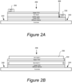
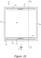
- Figures 2A and 2B are schematic illustrations of a construction, 200 , comprising an EC device fabricated on a substantially transparent substrate (e.g., glass substrate).
- Figure 2C is a top view schematic drawing of the construction in Figures 2A and 2B .
- Figure 2A depicts cross-section X-X'
- Figure 2B depicts view Y-Y' , as indicated in Figure 2C .
- the construction 200 shown in Figures 2A-2C is similar to the construction 100 shown in Figure 1 .
- the construction 200 includes an electrochromic (EC) device fabricated on the substrate.
- the EC device comprises a diffusion barrier disposed over a lower TCO and a buffer layer disposed over the lower TCO.
- the EC device further comprises an electrochromic stack disposed over the buffer layer.
- the EC stack includes an EC layer, an IC layer, and a CE layer.
- the EC device further comprises an upper TCO over the EC stack.
- the IC layer may be a separately deposited IC layer or may be an interfacial region created between the contacting and separately deposited EC and EC layers.
- a bus bar 1 230 is disposed on the upper TCO of the electrochromic device and a bus bar 2 232 is disposed on the lower TCO of the electrochromic device.
- the pair of bus bars, bus bar 1 230 and bus bar 2 232 are configured to be electrically connected to the corresponding TCOs in order to apply a voltage/current across the EC stack.
- edge deletion areas, 240 can be formed using laser ablation, for example, in an edge deletion operation to remove the material layers above the substrate to leave clean edges about the perimeter of the EC device.
- the edge delete width about the perimeter is between about 1 mm and about 20 mm wide.
- the edge delete width about the perimeter is between about 5 mm and about 15 mm wide.
- the edge delete width about the perimeter is between about 8 mm and about 10 mm wide.
- there are no laser isolation scribes used to isolate the active region from any inactive regions of the device stack that is, there are no inactive device regions in the final construct by virtue of not having to use laser isolation scribes.
- Such laser patterning is described in U.S. Patent Application 14/362,862 titled "THIN-DEVICES AND FABRICATION," and filed on June 4, 2014 , which is hereby incorporated by reference in its entirety.
- the illustrated example also depicts a bus pad expose (BPE) 260 in Figure 2C .
- the BPE 260 is a portion of the lower TCO that is exposed so that the bus bar 2 232 can be formed thereon and with electrical contact to the lower TCO.
- the portion of the layers of the EC device down to the lower TCO can be removed in a BPE operation to create a landing for the bus bar 2 232 .
- Formation of the edge delete areas 240 and BPE 260 can be performed in any order. In one embodiment, the edge deletion operation is performed before the BPE operation.
- a BPE (e.g., BPE 260 in Figure 2C ) can refer to a portion of the layers of an EC device that is removed down to the lower electrode (e.g. lower TCO) to create a surface for a bus bar to be applied and make electrical contact with the electrode.
- the bus bar applied can be a soldered bus bar, an ink bus bar, and the like.
- a BPE typically has a rectangular area, but this is not necessary; the BPE may be any geometrical shape or a random shape.
- a BPE may be circular, triangular, oval, trapezoidal, and other polygonal shapes. The shape may be dependent on the configuration of the EC device, the substrate bearing the EC device (e.g.
- the BPE substantially spans one side of an EC device and is wide enough to accommodate the bus bar with space at least between the EC device stack and the bus bar.
- the BPE is substantially rectangular, the length approximating one side of the EC device and the width is between about 5 mm and about 15 mm, in another embodiment between about 5 mm and about 10 mm, and in yet another embodiment between about 7 mm and about 9 mm.
- a bus bar may be between about 1 mm and about 5 mm wide, typically about 3 mm wide.
- the BPE is typically, but not necessarily, made wide enough to accommodate the bus bar's width and also leave space between the bus bar and the EC device (as the bus bar is only supposed to touch the lower electrode).
- the bus bar width may exceed that of the BPE (and thus there is bus bar material touching both lower conductor and glass), so long as there is space between the bus bar and the EC device.
- the outer edge, along the length, of the bus bar may be aligned with the outer edge of the BPE, or inset by about 1 mm to about 3 mm.
- the space between the bus bar and the EC device is between about 1 mm and about 3 mm, in another embodiment between about 1 mm and 2 mm, in another embodiment about 1.5 mm. Formation of BPE's is described in more detail below, with respect to an EC device having a lower electrode that is a TCO. This is for convenience only, the electrode could be any suitable electrode, transparent or not.
- an area over the lower electrode e.g., TCO
- TCO lower electrode
- this can be achieved by laser ablation of the material above a pre-treated buffer layer above the lower TCO. This can selectively remove the deposited material layers while leaving the lower TCO exposed in a defined area at a defined location (i.e. at the BPE).
- the relative absorption properties of the transparent lower electrode and the pre-treated sub-layer (e.g., buffer layer) and any layers deposited over the pre-treated sub-layer may be exploited in order to achieve selective removal during laser ablation to form the BPE. That is, pre-treating the sub-layer can increase its absorption properties.
- the pre-treated sub-layer will absorb the energy more readily and be selectively removed (or substantially removed) along with any material layers disposed on top of the sub-layer to leave the lower electrode (e.g. lower TCO) substantially intact.
- the upper portion of the lower electrode layer may also be removed in order to ensure good electrical contact of the bus bar with the lower electrode, that is, by removing any mixture of TCO and EC materials that might have occurred during deposition in that upper portion of the lower electrode.
- the same electromagnetic radiation (e.g., laser radiation) used to form the BPE can be used to perform edge deletion in the same EC device.
- the electromagnetic radiation from a laser source is delivered to the substantially transparent substrate using either optical fiber(s) or the open beam path.
- laser ablation can be performed from either substrate side or the film side depending on the choice of the electromagnetic radiation wavelength.
- the laser energy density required to ablate the material layer thickness is achieved by passing the laser beam through a lens. The lens focuses the laser beam to the desired shape and size. In one case, the energy density is between about 0.5 J/cm2 and about 4 J/cm2.
- Certain embodiments pertain to methods of fabricating an optical device, where each method comprises, in the following order: (a) exposing a sub-layer of the optical device to an energy source, (b) depositing one or more material layers of the optical device on the sub-layer, and (c) ablating the one or more material layers and the sub-layer with a laser to expose the underlying layer (e.g., a lower conductor layer).
- exposing the sub-layer to the energy source can alter the absorptive properties of the sub-layer and, in some cases, also the underlying material layer(s).
- (a) is performed only on a portion of the area of the sub-layer and (c) is performed substantially on the same corresponding portion of the sub-layer.
- ablation energy is applied, in this embodiment, to a portion of the top layer that is a perpendicular projection of the portion of the underlying layer that was pre-treated in step (a). This portion may define the area that is selectively ablated in (c).
- the energy source used in (a) may be the laser used in (c), may be another laser, or may be plasma.
- plasma etching using various gas plasmas, e.g. halogens such as fluorine, chlorine and/or bromine, is well known to remove material layers in electronic device fabrication.
- the optical device may be an electrochromic device.
- the method further comprises fabricating a bus bar on the lower conductor layer (e.g., lower TCO) that exposed in (c).
- the sub-layer comprises titanium dioxide (TiO 2 ) and, in some cases, the sub-layer may consist of TiO 2 .
- TiO 2 has proven useful in many electronic device applications, including optical device applications, yet without any pre-treatment, its absorption characteristics can make it difficult to ablate, especially after one or more material layers have been deposited on top of it.
- the pre-treatment methods of embodiments expose the sub-layer comprising TiO 2 to the energy source to increase the absorptive properties of this sub-layer, which may increase absorption of laser energy for less difficult ablation.
- the underlying layers may also receive energy from the energy source and its properties may change accordingly.
- the underlying layer comprises tin oxide (e.g., SnO 2 ) and receives energy, its absorptive properties may be decreased as a result.
- the sub-layer being pre-treated comprises TiO 2 and the underlying layer(s) comprises tin oxide.
- pre-treatment of the sub-layer comprising TiO 2 may increase the optical absorption of the TiO 2 sub-layer while simultaneously increasing the optical transmission of the underlying tin oxide layer.
- the electrochromic device may include a WO 3 electrochromic layer and a nickel-based counter electrode layer.
- Exemplary nickel-based counter electrode layers include doped NiO, e.g. NiWO, NiTaO, and the like.
- the sub-layer may be on top of and directly adjacent to, the lower conductor layer of the electrochromic device.
- the lower conductor layer includes tin oxide (e.g., SnO 2 ).
- TCOs transparent conductive oxides
- fluorinated tin oxides are formed on glass substrates and may serve as the lower conductor layer.
- conductive layer coated glasses are TEC Glass TM by Pilkington, of Toledo, Ohio and SUNGATE TM 300 and SUNGATE TM 500 by PPG Industries of Pittsburgh, Pennsylvania.
- TEC Glass TM is a glass coated with a fluorinated tin oxide conductive layer.
- the sub-layer being exposed to an energy source in step (a) may be a TiO 2 buffer film (i.e., a buffer film comprising that TiO 2 ) that is deposited adjacent to a lower transparent conductor layer of the electrochromic device.
- a TiO 2 buffer film i.e., a buffer film comprising that TiO 2
- the sub-layer in Figure 1 is the buffer layer 118 disposed over the lower TCO 120 of the illustrated electrochromic device.
- the sub-layer in Figures 2A- 2C is the buffer layer disposed over the lower TCO of the illustrated electrochromic device.
- these buffer layers may be TiO 2 buffer films.
- the TiO 2 buffer film may be subjected to a pre-treatment by an energy source prior to depositing the remaining electrochromic layers.
- the pre-treatment alters the characteristics of the TiO 2 , and enables selective removal using a laser source of the TiO 2 buffer film and the electrochromic film stack from the underlying TCO in the area that was pre-treated.
- the pre-treatment exposure can be via a laser source and/or a localized plasma.
- plasmas including atmospheric O 2 , N 2 /H 2 , halogens, or other gases, reactive or not, may be used (reactive plasmas may chemically change the TiO 2 film making more absorptive, while a nonreactive plasma may structurally alter the TiO 2 without necessarily changing it chemically.
- the pre-treatment area is then exposed to a laser source for ablation of the TiO 2 buffer film and electrochromic film stack thereon. Laser ablation results in uncovering the underlying TCO, allowing for good electrical contact with the bus bar applied to the exposed TCO.
- the sub-layer may be made of various materials and have various properties.
- the sub-layer may include, for example, a metal oxide, a metal nitride, a metal carbide, a metal oxynitride, or a metal oxycarbide.
- the sub-layer may comprise a metal oxide selected from the group consisting of aluminum oxide, titanium oxide, TiO 2 , tantalum oxide, cerium oxide, zinc oxide, tin oxide, silicon aluminum oxide, tungsten oxide, nickel tungsten oxide, and oxidized indium tin oxide.
- the sub-layer may comprise a metal nitride selected from the group consisting of titanium nitride, aluminum nitride, silicon nitride, tantalum nitride, and tungsten nitride.
- the sub-layer may comprise a metal carbide selected from the group consisting of titanium carbide, aluminum carbide, silicon carbide, tantalum carbide, and tungsten carbide.
- An example of a sub-layer that is a buffer layer in an electrochromic device is the defect-mitigating insulating layer described in U.S. Patent Application Serial No. 13/763,505 , entitled “DEFECT-MITIGATION LAYERS IN ELECTROCHROMIC DEVICES,” filed on February 8, 2013, which is hereby incorporated by reference in its entirety.
- the pre-treatment operation involves exposing at least a portion of the sub-layer of the optical device to an energy source.
- the energy source is a laser source.
- pre-treatment involves heating the sub-layer (e.g., TiO 2 layer) very quickly (for example, within 10-500 nanoseconds) to temperatures exceeding 400°C to increase the optical absorption properties of the sub-layer. In one case, the sub-layer is heated within 10-20 nanoseconds. If the sub-layer comprises TiO 2 and the underlying layer comprises tin oxide (e.g, SnO 2 ), the pre-treatment may increase optical absorption of the TiO 2 layer while simultaneously increasing the optical transmission of the underlying tin oxide.
- the sub-layer e.g., TiO 2 layer
- tin oxide e.g, SnO 2
- pre-treatment of a sub-layer comprising TiO 2 can also localize cracking of the TiO 2 at sufficient laser fluences.
- laser energy is more highly absorbed by the pre-treated sub-layer (e.g., TiO 2 layer) as compared to the un-treated sub-layer, so that pre-treatment increases selectivity of the process of removal of pre-treated sub-layer.
- the laser firing frequency during pre-treatment may be set to 10 kHz.
- the energy source is a plasma.
- pre-treatment involves exposing the surface of the sub-layer (e.g.., TiO 2 layer) to an atmospheric-pressure plasma, resulting in cracking of the surface and higher absorption of water into the underlying layer(s) of, for example, of a film stack.
- the plasma pre-treatment is performed selectively on an area or areas of the sub-layer (e.g., films) that are to be removed after optical device fabrication thereon.
- the morphology of the sub-layer results in higher absorption of the laser energy in the pre-treated areas, resulting in increased selectivity of the process to removal of sub-layer in the pre-treated areas.
- pre-treatment process includes the intentional alteration of a TiO 2 film or other sub-layer for increased laser absorption through alteration of material properties (extinction coefficient, optical absorption) and morphology (localized cracking / discontinuity) in the TiO 2 film or other sub-layer.
- material properties extinction coefficient, optical absorption
- morphology localized cracking / discontinuity
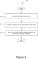
- FIG 3 is a flowchart of a process flow 400 describing aspects of a method of fabricating an optical device (e.g., electrochromic device) according to embodiments that involve pre-treating a sub-layer of the optical device.
- an optical device e.g., electrochromic device
- FIG. 3 is a flowchart of a process flow 400 describing aspects of a method of fabricating an optical device (e.g., electrochromic device) according to embodiments that involve pre-treating a sub-layer of the optical device.
- a surface of a sub-layer of an optical device is exposed to energy from an energy source.
- the energy source applied can be from a laser source and/or localized plasma (e.g., atmospheric O 2 , N 2 /H 2 , halogens or other gases may be used).
- the sub-layer is disposed over an underlying layer(s).
- the sub-layer may comprise TiO 2 and/or the underlying layer may comprise SnO 2 .
- the sub-layer may be a buffer layer (e.g., buffer layer 118 in Figure 1 ) over a lower TCO or may be a layer (e.g., diffusion layer) over the substantially transparent substrate. Exposing the sub-layer to the energy source may alter the properties and/or morphology of the sub-layer and/or the underlying layer(s), particularly the absorptive properties as described herein.
- a portion of the surface area of the sub-layer is exposed to the energy source in step 410 .
- This portion can define the desired area that will be selectively removed (e.g., ablated) in step 430 .
- An example of a portion of a sub-layer that may be exposed in step 410 is the BPE 260 on the lower TCO, which is shown in Figures 2A-2C .
- Another example of portions of a sub-layer are edge delete areas 240 that may be located on a layer (e.g., diffusion layer) over the substantially transparent substrate. In certain cases, this portion may be about or slightly larger than the area that is desired to be removed later.
- the initially exposed area slightly larger than the area that is ultimately removed, a perimeter of the exposed material is left behind.
- This peripheral material might then act as an insulating material between a bus bar and the device stack to ensure the bus bar does not make direct contact with the edge of the device stack layers (overlying the TCO to which it does make electrical connection).
- This peripheral material might also act to "contain" bus bar ink prior to curing, as it is higher in profile and may surround the area where the bus bar ink is deposited or at least serve as a dam to impede the flow of bus bar ink toward the device stack.
- step 420 one or more material layers are deposited on the pre-treated sub-layer.
- step 420 may comprise depositing the EC stack and/or upper TCO over the pre-treated sub-layer such as, for example, to form the EC device shown in Figure 1 or Figures 2A -2C .
- the optical device is ablated with a laser source to at least substantially remove the pre-treated sub-layer and the one or more material layers deposited over the pre-treated layer.
- the laser source used in this step 430 for ablation may be the same energy source used in step 410 .
- step 430 only a portion of the sub-layer and overlying layer(s) is ablated in step 430 .
- the ablation energy may be applied to a selected area of the optical device that is desired to be removed. In certain aspects, this selected area may correspond to the portion of the sub-layer that was pre-treated (exposed) in step 410 .
- An illustrated example of area of an electrochromic device that may be selected for ablation is the BPE 260 shown in Figure 2C .
- step 430 may comprise removing the buffer layer over the lower TCO and the material layers of an electrochromic film stack and/or upper TCO over the buffer layer. This step may result in revealing the underlying conductive TCO appropriately (e.g.
- step 430 the pre-treated sub-layer and overlying layer(s) are substantially removed, some de minimus amount of material from these layers may remain. This residual material may be removed in additional operations, for example, by mechanical means, by additional ablation operations, etc. In other cases, the pre-treated sub-layer and overlying layer(s) are cleanly removed in step 430 .
- the illustrated method shown in Figure 3 may include additional processing steps used in fabricating optical devices.
- the method may further comprise fabricating a bus bar over the underlying layer exposed in step 430 .
- the underlying layer is a lower conductor (e.g., lower TCO in Figures 1 , 2A, and 2B ). Additional processing steps that can be included in the illustrated method can be found in PCT International Application No. PCT/US2012/068817, titled “THIN-FILM DEVICES AND FABRICATION,” and filed on December 10, 2012 , and U.S. Patent Application No. 13/456,056, titled “ELECTROCHROMIC WINDOW FABRICATION METHODS,” filed on April 25, 2012 .
- methods of embodiments described herein can selectively remove thin films from an optical device to reveal underlying transparent conductor layers. These methods can be used to selectively remove material layers from an electrochromic device to reveal the lower TCO layer, for example.
- the lower TCO may need to be locally exposed for application of a bus bar to the exposed area.
- the method may be exposing the lower TCO layer and the sub-layer being pre-treated may comprise one or more buffer layers (e.g., SnO 2 and TiO 2 buffer films) deposited over the lower TCO, for example, prior to depositing the electrochromic film stack.
- the pre-treatment alters the characteristics of the TiO 2 and hence enables selective removal of the TiO 2 and any layers deposited on the buffer layer(s) from the underlying TCO layer using a laser source.
- the electrochromic film stack may be deposited over the pre-treated buffer layer(s), and the pre-treatment area is exposed to a laser source for ablation of the TiO 2 and electrochromic film stack. The results in exposure of the underlying lower TCO, which can allow for good electrical contact with a bus bar applied to the exposed area of the TCO.
- the EC device includes a buffer layer comprising TiO 2 (i.e. a TiO 2 layer) on a lower TCO (of, e.g., fluorinated tin oxide).
- the EC stack includes an electrochromic layer (e.g., WO 3 layer) a counter electrode layer (e.g., NiWO) and an upper TCO (indium tin oxide) in the thickness shown.
- electrochromic layer e.g., WO 3 layer
- a counter electrode layer e.g., NiWO
- an upper TCO indium tin oxide
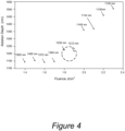
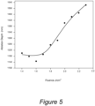
- Figures 4 and 5 show the graphical results of the ablation depth vs. fluence (i.e., laser energy), using high pattern overlap and high spot overlap, respectively.
- High overlap in this context means that a significant amount of the laser pattern or spot was overlapped with subsequent laser patterns or spots in order to accomplish the desired ablation depth (e.g., about 1200nm).
- High spot overlap results in higher heating and therefore less fluence is required to ablate the material layers to the desired 1200 nm ablation depth.
- a very narrow process window results in the control experiments.
- ablation depth that is close to 1200 nm as shown by the dotted circle could only be achieved with application of laser fluence at about 1.8 and 1.9 J/cm 2 , that is, within a tight range of 0.1 J/cm 2 .
- an ablation depth of about 1200 nm was achieved only with application of laser fluence between 1.7 and 1.80 J/cm 2 , again within a tight range of only 0.1 J/cm 2 .
- the data point at fluence level of 1.4 J/cm2 may be high due to measurement noise.
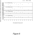
- Pre-treating the sub-layer can widen the process window of the laser fluence levels needed to ablate to the desired ablation depth. That is, the range of laser fluence levels that can be used to accomplish a desired laser ablation depth may be widened if pre-treatment is used on the sub-layer being ablated. For example, with reference to the electrochromic device used in the experiments in this section, by pretreating the TiO 2 buffer layer prior to depositing the remaining material layers of the electrochromic device, and then laser ablating, a much wider process window can be achieved in the removal step. This is shown in Figure 6 . The x-axis of the graph in Figure 6 represents pre-treatment laser fluence levels applied to the TiO 2 buffer layer in the electrochromic device.
- the ⁇ -axis shows the ablation depth at four laser ablation fluence levels: (1) 1.8 J/cm 2 , (2) 1.9 J/cm 2 , (3) 2.0 J/cm 2 , and (4) 2.3 J/cm 2 .
- the results show the different ablation depths achieved by these four laser ablation fluence levels (y-axis) based the fluence level used to pre-treat the sub-layer (x-axis).
- the dotted lines in the x-direction denote the desired target ablation depth of 1200 nm.
- the range of ablation fluence levels for the desired ablation depth was increased (doubled) as compared to control - a much larger process window for ablation was achieved using pre-treatment of the sub-layer (and the pre-treatment has a wide process window as well, between 1.0 and 2.2 J/cm 2 fluence levels).
- a sacrificial material layer is applied to a selected area of the one or more sub-layers of an optical device.
- the material and thickness used in this sacrificial material layer are selected to provide desired absorptive properties) that allow for control over the thermal flux once the laser ablation of the selected area is performed.
- the material and thickness of the sacrificial material layer may be selected to control the thermal flux to a bus bar pad expose of a buffer layer in order to expose a lower TCO for bus bar application in an electrochromic device.
- certain embodiments are directed to a method of fabricating an optical device that includes applying a sacrificial material layer during the deposition process.
- the method comprises: i) applying a sacrificial material layer (e.g., thin film) to one or more sub-layers of the optical device; where the sacrificial material layer is applied only to a portion of the area of the one or more sub-layers of the optical device; ii) depositing one or more material layers of the optical device on the sacrificial material layer and the one or more sub-layers; and iii) applying a laser to the portion to ablate the optical device at least down to the sacrificial material layer.
- the optical device can be an electrochromic device.
- the one or more sub-layers may include a buffer layer such as a buffer layer comprising TiO 2 .
- the electrochromic device includes a WO 3 electrochromic layer and a nickel-based counter electrode layer.
- the nickel-based counter electrode layer may include NiWO or NiTaO.
- the one or more sub-layers are on top of and directly adjacent to, the lower conductor layer (e.g., lower TCO) of the electrochromic device.
- the lower conductor layer may comprise SnO 2 .
- the lower conductor layer is substantially intact after iii).
- the method further includes fabricating a bus bar on the lower conductor layer exposed in iii).
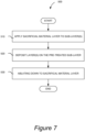
- Figure 7 is a flowchart of a process flow 500 describing aspects of a method of fabricating an optical device (e.g., electrochromic device) according to embodiments that involve applying a sacrificial material layer to a sub-layer.
- an optical device e.g., electrochromic device
- FIG. 7 is a flowchart of a process flow 500 describing aspects of a method of fabricating an optical device (e.g., electrochromic device) according to embodiments that involve applying a sacrificial material layer to a sub-layer.
- a sacrificial material layer is applied to one or more sub-layers of an optical device.
- the material and thickness of the sacrificial material layer may be selected to provide a desired absorptive property for a predefined thermal flux that will be used in laser ablation in step 530.
- the sacrificial material layer is applied only to a portion of the available surface area of the one or more sub-layers of the optical device. This portion corresponds approximately to the area that will be targeted in the laser ablation in step 530 .
- step 520 one or more material layers are deposited on the sacrificial material layer.
- step 420 may comprise depositing the EC stack and/or upper TCO over the sacrificial material layer such as, for example, to form the EC device similar to the one shown in Figure 1 or Figures 2A -2C .
- energy fluence form a laser is directed to the portion of the sacrificial material layer to ablate the optical device down to at least the sacrificial material layer.
- the sacrificial material layer and overlying layer(s) are at least substantially removed. That is, in some cases, some material from these layers may remain. This residual material may be removed in additional operations, for example, by mechanical means, by additional ablation operations, etc. In other cases, the sacrificial material layer and overlying layer(s) are cleanly removed in step 530 .
Landscapes
- Physics & Mathematics (AREA)
- Nonlinear Science (AREA)
- General Physics & Mathematics (AREA)
- Optics & Photonics (AREA)
- Electrochromic Elements, Electrophoresis, Or Variable Reflection Or Absorption Elements (AREA)
- Laser Beam Processing (AREA)
- Chemical & Material Sciences (AREA)
- Inorganic Chemistry (AREA)
- Manufacturing Of Electric Cables (AREA)
- Non-Insulated Conductors (AREA)
Applications Claiming Priority (3)
| Application Number | Priority Date | Filing Date | Title |
|---|---|---|---|
| US201361834372P | 2013-06-12 | 2013-06-12 | |
| PCT/US2014/042178 WO2014201287A1 (fr) | 2013-06-12 | 2014-06-12 | Prétraitement de couches minces d'oxyde conducteur transparent (oct) pour améliorer le contact électrique |
| EP14810785.7A EP3008514B1 (fr) | 2013-06-12 | 2014-06-12 | Prétraitement de couches minces d'oxyde conducteur transparent (oct) pour améliorer le contact électrique |
Related Parent Applications (1)
| Application Number | Title | Priority Date | Filing Date |
|---|---|---|---|
| EP14810785.7A Division EP3008514B1 (fr) | 2013-06-12 | 2014-06-12 | Prétraitement de couches minces d'oxyde conducteur transparent (oct) pour améliorer le contact électrique |
Publications (2)
| Publication Number | Publication Date |
|---|---|
| EP4258047A2 true EP4258047A2 (fr) | 2023-10-11 |
| EP4258047A3 EP4258047A3 (fr) | 2023-11-08 |
Family
ID=52022781
Family Applications (2)
| Application Number | Title | Priority Date | Filing Date |
|---|---|---|---|
| EP23188618.5A Pending EP4258047A3 (fr) | 2013-06-12 | 2014-06-12 | Prétraitement de couches minces d'oxyde conducteur transparent (oct) pour améliorer le contact électrique |
| EP14810785.7A Active EP3008514B1 (fr) | 2013-06-12 | 2014-06-12 | Prétraitement de couches minces d'oxyde conducteur transparent (oct) pour améliorer le contact électrique |
Family Applications After (1)
| Application Number | Title | Priority Date | Filing Date |
|---|---|---|---|
| EP14810785.7A Active EP3008514B1 (fr) | 2013-06-12 | 2014-06-12 | Prétraitement de couches minces d'oxyde conducteur transparent (oct) pour améliorer le contact électrique |
Country Status (7)
| Country | Link |
|---|---|
| US (4) | US10656492B2 (fr) |
| EP (2) | EP4258047A3 (fr) |
| KR (2) | KR102521229B1 (fr) |
| CN (2) | CN105324707B (fr) |
| CA (1) | CA2914763C (fr) |
| HK (1) | HK1223687A1 (fr) |
| WO (1) | WO2014201287A1 (fr) |
Families Citing this family (36)
| Publication number | Priority date | Publication date | Assignee | Title |
|---|---|---|---|---|
| US10261381B2 (en) | 2009-03-31 | 2019-04-16 | View, Inc. | Fabrication of low defectivity electrochromic devices |
| US10852613B2 (en) | 2009-03-31 | 2020-12-01 | View, Inc. | Counter electrode material for electrochromic devices |
| US9664974B2 (en) | 2009-03-31 | 2017-05-30 | View, Inc. | Fabrication of low defectivity electrochromic devices |
| US12043890B2 (en) | 2009-03-31 | 2024-07-23 | View, Inc. | Electrochromic devices |
| US10156762B2 (en) | 2009-03-31 | 2018-12-18 | View, Inc. | Counter electrode for electrochromic devices |
| US10591795B2 (en) | 2009-03-31 | 2020-03-17 | View, Inc. | Counter electrode for electrochromic devices |
| US8582193B2 (en) | 2010-04-30 | 2013-11-12 | View, Inc. | Electrochromic devices |
| US9007674B2 (en) | 2011-09-30 | 2015-04-14 | View, Inc. | Defect-mitigation layers in electrochromic devices |
| US12353109B2 (en) | 2009-12-22 | 2025-07-08 | View Operating Corporation | Electrochromic cathode materials |
| US9759975B2 (en) | 2010-04-30 | 2017-09-12 | View, Inc. | Electrochromic devices |
| US9958750B2 (en) | 2010-11-08 | 2018-05-01 | View, Inc. | Electrochromic window fabrication methods |
| US12496809B2 (en) | 2010-11-08 | 2025-12-16 | View Operating Corporation | Electrochromic window fabrication methods |
| US11865632B2 (en) | 2011-12-12 | 2024-01-09 | View, Inc. | Thin-film devices and fabrication |
| US10295880B2 (en) | 2011-12-12 | 2019-05-21 | View, Inc. | Narrow pre-deposition laser deletion |
| US10802371B2 (en) | 2011-12-12 | 2020-10-13 | View, Inc. | Thin-film devices and fabrication |
| US12061402B2 (en) | 2011-12-12 | 2024-08-13 | View, Inc. | Narrow pre-deposition laser deletion |
| CA2859023C (fr) | 2011-12-12 | 2023-08-22 | View, Inc. | Dispositifs en couches minces et fabrication de ceux-ci |
| US12403676B2 (en) | 2011-12-12 | 2025-09-02 | View Operating Corporation | Thin-film devices and fabrication |
| WO2014201287A1 (fr) | 2013-06-12 | 2014-12-18 | View, Inc. | Prétraitement de couches minces d'oxyde conducteur transparent (oct) pour améliorer le contact électrique |
| US11891327B2 (en) | 2014-05-02 | 2024-02-06 | View, Inc. | Fabrication of low defectivity electrochromic devices |
| US10345671B2 (en) | 2014-09-05 | 2019-07-09 | View, Inc. | Counter electrode for electrochromic devices |
| US12235560B2 (en) | 2014-11-25 | 2025-02-25 | View, Inc. | Faster switching electrochromic devices |
| CN116789175A (zh) | 2014-11-26 | 2023-09-22 | 唯景公司 | 用于电致变色装置的对电极 |
| EP3238253B1 (fr) * | 2014-12-24 | 2021-10-27 | View, Inc. | Methode de fabrication d'un bus bar pad et dispositif optique comprenant un bus bar pad |
| CN107533267A (zh) | 2015-03-20 | 2018-01-02 | 唯景公司 | 更快速地切换低缺陷电致变色窗 |
| US10035139B2 (en) | 2015-06-29 | 2018-07-31 | Korea Advanced Institute Of Science And Technology | Method for improving solar energy conversion efficiency using metal oxide photocatalysts having energy band of core-shell for ultraviolet ray and visible light absorption and photocatalysts thereof |
| CN119916619A (zh) * | 2015-07-14 | 2025-05-02 | 唯景公司 | 用于电致变色装置的对电极 |
| CA3026244A1 (fr) * | 2016-06-01 | 2017-12-07 | View, Inc. | Couche sacrificielle destinee a la fabrication de dispositifs electrochromiques |
| US11623433B2 (en) | 2016-06-17 | 2023-04-11 | View, Inc. | Mitigating defects in an electrochromic device under a bus bar |
| CN110337716A (zh) | 2017-02-27 | 2019-10-15 | Sage电致变色显示有限公司 | 包括基板和透明导电层的电气设备及形成电气设备的方法 |
| CN111226163B (zh) * | 2017-11-03 | 2021-10-22 | 伊英克公司 | 用于生产电光显示器的工艺 |
| CN107943211A (zh) * | 2017-11-30 | 2018-04-20 | 维沃移动通信有限公司 | 终端设备及其控制方法 |
| US10996535B1 (en) * | 2018-11-07 | 2021-05-04 | Eclipse Energy Systems, Inc. | Electrochromic device with buffer layer(s) |
| US12066734B1 (en) | 2018-11-07 | 2024-08-20 | Eclipse Energy Systems, Inc. | Electrochromic device having various uses |
| CN114787705A (zh) | 2019-12-10 | 2022-07-22 | 唯景公司 | 用于处理电致变色玻璃的激光方法 |
| CN119270553A (zh) * | 2024-10-15 | 2025-01-07 | 北京理工大学 | 包含参比电极的电致变色器件结构和制备方法 |
Citations (1)
| Publication number | Priority date | Publication date | Assignee | Title |
|---|---|---|---|---|
| US8300298B2 (en) | 2010-04-30 | 2012-10-30 | Soladigm, Inc. | Electrochromic devices |
Family Cites Families (36)
| Publication number | Priority date | Publication date | Assignee | Title |
|---|---|---|---|---|
| US5353705A (en) * | 1992-07-20 | 1994-10-11 | Presstek, Inc. | Lithographic printing members having secondary ablation layers for use with laser-discharge imaging apparatus |
| FR2781084B1 (fr) | 1998-07-10 | 2007-08-31 | Saint Gobain Vitrage | Procede de traitement d'un dispositif electrochimique |
| JP2000075319A (ja) * | 1998-08-26 | 2000-03-14 | Sharp Corp | アクティブマトリクス基板の欠陥修正方法、製造方法及び欠陥修正装置 |
| US7255451B2 (en) | 2002-09-20 | 2007-08-14 | Donnelly Corporation | Electro-optic mirror cell |
| JP4509720B2 (ja) | 2002-03-12 | 2010-07-21 | 浜松ホトニクス株式会社 | レーザ加工方法 |
| US6743524B2 (en) | 2002-05-23 | 2004-06-01 | General Electric Company | Barrier layer for an article and method of making said barrier layer by expanding thermal plasma |
| WO2004091842A1 (fr) * | 2003-04-11 | 2004-10-28 | Lpkf Laser & Electronics Ag | Procede de realisation de systemes multicouches |
| CN100527423C (zh) * | 2004-10-20 | 2009-08-12 | 茂德科技股份有限公司 | 自我对准非挥发性存储器及其制造方法 |
| US7160745B2 (en) * | 2004-10-28 | 2007-01-09 | Hewlett-Packard Development Company, L.P. | Metal-insulator-metal device |
| JP2006155920A (ja) * | 2004-11-25 | 2006-06-15 | Denso Corp | El素子の製造方法 |
| US20060183055A1 (en) * | 2005-02-15 | 2006-08-17 | O'neill Mark L | Method for defining a feature on a substrate |
| US7593154B2 (en) * | 2005-10-11 | 2009-09-22 | Sage Electrochromics, Inc. | Electrochromic devices having improved ion conducting layers |
| WO2007049939A1 (fr) * | 2005-10-29 | 2007-05-03 | Samsung Electronics Co., Ltd. | Dispositif semi-conducteur et procede de fabrication |
| US20070210420A1 (en) * | 2006-03-11 | 2007-09-13 | Nelson Curt L | Laser delamination of thin metal film using sacrificial polymer layer |
| TWI427682B (zh) * | 2006-07-04 | 2014-02-21 | 半導體能源研究所股份有限公司 | 顯示裝置的製造方法 |
| EP2069419A2 (fr) | 2006-08-24 | 2009-06-17 | E.I. Du Pont De Nemours And Company | Polymères transportant les trous |
| US7767595B2 (en) * | 2006-10-26 | 2010-08-03 | Semiconductor Energy Laboratory Co., Ltd. | Manufacturing method of semiconductor device |
| WO2009139376A1 (fr) | 2008-05-14 | 2009-11-19 | 昭和電工株式会社 | Procédé de production d’un élément électroluminescent semi-conducteur en nitrure de groupe iii, élément électroluminescent semi-conducteur en nitrure de groupe iii et lampe |
| US8168265B2 (en) | 2008-06-06 | 2012-05-01 | Applied Materials, Inc. | Method for manufacturing electrochromic devices |
| US7911674B2 (en) * | 2008-12-29 | 2011-03-22 | Soladigm, Inc. | Electrochromic devices and methods for patterning such devices |
| KR20100092745A (ko) * | 2009-02-13 | 2010-08-23 | 엘지전자 주식회사 | 전기 변색 장치 |
| WO2013049379A1 (fr) * | 2011-09-30 | 2013-04-04 | Soladigm, Inc | Fabrication de dispositif optique amélioré |
| US9007674B2 (en) | 2011-09-30 | 2015-04-14 | View, Inc. | Defect-mitigation layers in electrochromic devices |
| WO2012177790A2 (fr) * | 2011-06-21 | 2012-12-27 | Soladigm, Inc. | Dispositifs électrochromiques aptes à être trempés |
| US9664974B2 (en) * | 2009-03-31 | 2017-05-30 | View, Inc. | Fabrication of low defectivity electrochromic devices |
| US20100291431A1 (en) | 2009-05-13 | 2010-11-18 | Front Edge Technology, Inc. | Thin film battery with protective packaging |
| JP5596312B2 (ja) * | 2009-08-04 | 2014-09-24 | スタンレー電気株式会社 | 誘電体薄膜デバイスの製造方法 |
| US8610991B2 (en) | 2010-07-14 | 2013-12-17 | Samsung Electronics Co., Ltd. | Electrochromic material and electrochromic device including the same |
| TWI542931B (zh) * | 2010-08-11 | 2016-07-21 | 友達光電股份有限公司 | 畫素結構之修補方法、修補後之畫素結構以及畫素陣列 |
| US9958750B2 (en) * | 2010-11-08 | 2018-05-01 | View, Inc. | Electrochromic window fabrication methods |
| CN102582159B (zh) * | 2011-01-14 | 2015-10-21 | 永恒科技有限公司 | 提供双色表面的板材及其形成方法 |
| WO2013106082A2 (fr) | 2011-06-17 | 2013-07-18 | Applied Materials, Inc. | Fabrication sans masque de batterie à couche mince |
| CN105789680B (zh) * | 2011-08-08 | 2019-05-28 | 应用材料公司 | 具有用于激光图案化的集成光热阻挡层的薄膜结构和装置 |
| CA2859023C (fr) | 2011-12-12 | 2023-08-22 | View, Inc. | Dispositifs en couches minces et fabrication de ceux-ci |
| TWI612712B (zh) | 2012-10-25 | 2018-01-21 | 應用材料股份有限公司 | 繞射光學元件及用於圖案化薄膜電化學元件的方法 |
| WO2014201287A1 (fr) | 2013-06-12 | 2014-12-18 | View, Inc. | Prétraitement de couches minces d'oxyde conducteur transparent (oct) pour améliorer le contact électrique |
-
2014
- 2014-06-12 WO PCT/US2014/042178 patent/WO2014201287A1/fr not_active Ceased
- 2014-06-12 KR KR1020217029726A patent/KR102521229B1/ko active Active
- 2014-06-12 CA CA2914763A patent/CA2914763C/fr active Active
- 2014-06-12 EP EP23188618.5A patent/EP4258047A3/fr active Pending
- 2014-06-12 KR KR1020157035064A patent/KR20160019438A/ko not_active Ceased
- 2014-06-12 US US14/893,504 patent/US10656492B2/en active Active
- 2014-06-12 EP EP14810785.7A patent/EP3008514B1/fr active Active
- 2014-06-12 HK HK16111860.6A patent/HK1223687A1/zh unknown
- 2014-06-12 CN CN201480033512.6A patent/CN105324707B/zh active Active
- 2014-06-12 CN CN202010430270.1A patent/CN111505881A/zh active Pending
-
2020
- 2020-03-20 US US16/826,086 patent/US11513411B2/en active Active
-
2022
- 2022-10-25 US US18/049,626 patent/US11762254B2/en active Active
-
2023
- 2023-08-18 US US18/452,427 patent/US12072599B2/en active Active
Patent Citations (1)
| Publication number | Priority date | Publication date | Assignee | Title |
|---|---|---|---|---|
| US8300298B2 (en) | 2010-04-30 | 2012-10-30 | Soladigm, Inc. | Electrochromic devices |
Also Published As
| Publication number | Publication date |
|---|---|
| CA2914763A1 (fr) | 2014-12-18 |
| CN111505881A (zh) | 2020-08-07 |
| US12072599B2 (en) | 2024-08-27 |
| EP3008514B1 (fr) | 2023-08-02 |
| US11762254B2 (en) | 2023-09-19 |
| US20230393442A1 (en) | 2023-12-07 |
| WO2014201287A1 (fr) | 2014-12-18 |
| US10656492B2 (en) | 2020-05-19 |
| HK1223687A1 (zh) | 2017-08-04 |
| CA2914763C (fr) | 2023-08-29 |
| CN105324707B (zh) | 2020-06-12 |
| CN105324707A (zh) | 2016-02-10 |
| KR102521229B1 (ko) | 2023-04-12 |
| KR20160019438A (ko) | 2016-02-19 |
| EP4258047A3 (fr) | 2023-11-08 |
| EP3008514A4 (fr) | 2017-02-22 |
| US20160109777A1 (en) | 2016-04-21 |
| US20230074891A1 (en) | 2023-03-09 |
| EP3008514A1 (fr) | 2016-04-20 |
| US11513411B2 (en) | 2022-11-29 |
| US20200218124A1 (en) | 2020-07-09 |
| KR20210117356A (ko) | 2021-09-28 |
Similar Documents
| Publication | Publication Date | Title |
|---|---|---|
| US12072599B2 (en) | Pretreatment of transparent conductive oxide (TCO) thin films for improved electrical contact | |
| US20220244609A1 (en) | Electrochromic devices on non-rectangular shapes | |
| US11559852B2 (en) | Thin-film devices and fabrication | |
| US11086182B2 (en) | Narrow pre-deposition laser deletion | |
| AU2020250303B2 (en) | Thin-film devices and fabrication | |
| TWI628499B (zh) | 電致變色裝置及製造彼之方法及裝置 | |
| EP3164762B1 (fr) | Suppression par laser de pré-dépôt étroit | |
| US20250093723A1 (en) | Narrow pre-deposition laser deletion | |
| US11865632B2 (en) | Thin-film devices and fabrication |
Legal Events
| Date | Code | Title | Description |
|---|---|---|---|
| PUAI | Public reference made under article 153(3) epc to a published international application that has entered the european phase |
Free format text: ORIGINAL CODE: 0009012 |
|
| STAA | Information on the status of an ep patent application or granted ep patent |
Free format text: STATUS: THE APPLICATION HAS BEEN PUBLISHED |
|
| PUAL | Search report despatched |
Free format text: ORIGINAL CODE: 0009013 |
|
| AC | Divisional application: reference to earlier application |
Ref document number: 3008514 Country of ref document: EP Kind code of ref document: P |
|
| AK | Designated contracting states |
Kind code of ref document: A2 Designated state(s): AL AT BE BG CH CY CZ DE DK EE ES FI FR GB GR HR HU IE IS IT LI LT LU LV MC MK MT NL NO PL PT RO RS SE SI SK SM TR |
|
| RIN1 | Information on inventor provided before grant (corrected) |
Inventor name: PRADHAN, ANSHU A. Inventor name: STRONG, FABIAN Inventor name: DIXIT, ABHISHEK ANANT Inventor name: MARTIN, TODD |
|
| AK | Designated contracting states |
Kind code of ref document: A3 Designated state(s): AL AT BE BG CH CY CZ DE DK EE ES FI FR GB GR HR HU IE IS IT LI LT LU LV MC MK MT NL NO PL PT RO RS SE SI SK SM TR |
|
| RIC1 | Information provided on ipc code assigned before grant |
Ipc: G02F 1/15 20190101AFI20230929BHEP |
|
| STAA | Information on the status of an ep patent application or granted ep patent |
Free format text: STATUS: REQUEST FOR EXAMINATION WAS MADE |
|
| 17P | Request for examination filed |
Effective date: 20240424 |
|
| RBV | Designated contracting states (corrected) |
Designated state(s): AL AT BE BG CH CY CZ DE DK EE ES FI FR GB GR HR HU IE IS IT LI LT LU LV MC MK MT NL NO PL PT RO RS SE SI SK SM TR |
|
| STAA | Information on the status of an ep patent application or granted ep patent |
Free format text: STATUS: EXAMINATION IS IN PROGRESS |
|
| 17Q | First examination report despatched |
Effective date: 20250716 |