EP4258100A2 - Pipelines de traitement multiplicateur-accumulateur et composant de traitement, et leurs procédés de fonctionnement - Google Patents
Pipelines de traitement multiplicateur-accumulateur et composant de traitement, et leurs procédés de fonctionnement Download PDFInfo
- Publication number
- EP4258100A2 EP4258100A2 EP23188233.3A EP23188233A EP4258100A2 EP 4258100 A2 EP4258100 A2 EP 4258100A2 EP 23188233 A EP23188233 A EP 23188233A EP 4258100 A2 EP4258100 A2 EP 4258100A2
- Authority
- EP
- European Patent Office
- Prior art keywords
- multiplier
- data
- accumulator
- processing
- memory
- Prior art date
- Legal status (The legal status is an assumption and is not a legal conclusion. Google has not performed a legal analysis and makes no representation as to the accuracy of the status listed.)
- Granted
Links
Images










Classifications
-
- G—PHYSICS
- G06—COMPUTING OR CALCULATING; COUNTING
- G06F—ELECTRIC DIGITAL DATA PROCESSING
- G06F9/00—Arrangements for program control, e.g. control units
- G06F9/06—Arrangements for program control, e.g. control units using stored programs, i.e. using an internal store of processing equipment to receive or retain programs
- G06F9/30—Arrangements for executing machine instructions, e.g. instruction decode
- G06F9/30003—Arrangements for executing specific machine instructions
- G06F9/30007—Arrangements for executing specific machine instructions to perform operations on data operands
- G06F9/3001—Arithmetic instructions
-
- G—PHYSICS
- G06—COMPUTING OR CALCULATING; COUNTING
- G06F—ELECTRIC DIGITAL DATA PROCESSING
- G06F7/00—Methods or arrangements for processing data by operating upon the order or content of the data handled
- G06F7/38—Methods or arrangements for performing computations using exclusively denominational number representation, e.g. using binary, ternary, decimal representation
- G06F7/48—Methods or arrangements for performing computations using exclusively denominational number representation, e.g. using binary, ternary, decimal representation using non-contact-making devices, e.g. tube, solid state device; using unspecified devices
- G06F7/544—Methods or arrangements for performing computations using exclusively denominational number representation, e.g. using binary, ternary, decimal representation using non-contact-making devices, e.g. tube, solid state device; using unspecified devices for evaluating functions by calculation
- G06F7/5443—Sum of products
-
- G—PHYSICS
- G06—COMPUTING OR CALCULATING; COUNTING
- G06F—ELECTRIC DIGITAL DATA PROCESSING
- G06F17/00—Digital computing or data processing equipment or methods, specially adapted for specific functions
- G06F17/10—Complex mathematical operations
Definitions
- the present inventions are directed to one or more integrated circuits having multiplier-accumulator circuitry (and methods of operating such circuitry) including a plurality of multiplier-accumulator execution or processing pipelines wherein each pipeline includes a plurality of multiplier-accumulator circuits that function or operate concurrently.
- the multiplier-accumulator execution or processing pipelines concurrently process related data (e.g., image data) via the plurality of separate multiplier-accumulator circuits (referred to herein, at times, as "MAC” or "MAC circuits”) and, in one embodiment, a plurality of registers (including a plurality of shadow registers) that facilitate pipelining of the multiply and accumulate operations to increase throughput of the multiplier-accumulator execution or processing pipelines in connection with processing the related data.
- the one or more integrated circuits each include a plurality of clusters (e.g., four) wherein each cluster includes a plurality of MAC execution pipelines (e.g., 16) wherein each MAC execution pipeline includes a plurality of separate multiplier-accumulator circuits (e.g., 64).
- the plurality of clusters may form a component (such component is often identified in the figures as “X1" or “X1 component”) that includes, in one embodiment, memory, a switch interconnect network to interconnect circuitry of the component (e.g., MAC execution pipeline(s) of the cluster(s) of the X1 component) and/or interconnect circuitry of the component with circuitry of one or more other X1 components, and interface circuitry (e.g., PHY and/or GPIO circuitry) to interface with, for example, external memory (e.g., DRAM, MRAM, SRAM and/or Flash memory).
- a switch interconnect network to interconnect circuitry of the component
- interconnect circuitry of the component e.g., MAC execution pipeline(s) of the cluster(s) of the X1 component
- interface circuitry e.g., PHY and/or GPIO circuitry
- one or more MAC execution pipelines of a plurality of clusters of a X1 component may be configured to concurrently process related data (e.g., image data) via the plurality of separate multiplier-accumulator circuits of each MAC execution pipeline.
- the MAC execution pipeline may be any size (e.g., 16, 32, 64, 96 or 128 multiplier-accumulator circuits) - which may be fixed (e.g., at manufacture) or configurable (e.g., one-time configurable or multiple-time configurable (e.g., at power-up and/or in situ).
- the one or more integrated circuits include a plurality of components or X1 components (e.g., 2, 4, ...), wherein each component includes a plurality of the clusters wherein each cluster includes a plurality of MAC execution pipelines.
- one integrated circuit includes a plurality of components or X1 components (e.g., 4 clusters) wherein each cluster includes a plurality of execution or processing pipelines (e.g., 16, 32 or 64) which are configured to process, function and/or operate concurrently such that related data is processed by each of the execution pipelines of a plurality of the clusters concurrently to, for example, decrease the processing time of the related data and/or increase data throughput of the X1 components.
- a plurality of execution or processing pipelines of each of the clusters of a plurality of the X1 components may be interconnected, for example, in a ring configuration or architecture to concurrently process related data (e.g., image data).
- a plurality of MAC execution pipelines of one or more (or all) of the clusters of a plurality of X1 components may be interconnected in a ring configuration or architecture to concurrently process related data.
- a plurality of MAC execution pipelines of one or more (or all) of the clusters of each X1 component are configured to process one or more stages of an image frame such that circuitry of each X1 component processes one or more stages of each image frame of a plurality of image frames.
- a plurality of MAC execution pipelines of one or more (or all) of the clusters of each X1 component are configured to process one or more portions of each stage of each image frame such that circuitry of each X1 component is configured to process a portion of each stage of each image frame of a plurality of image frames.
- a plurality of MAC execution pipelines of one or more (or all) of the clusters of each X1 component are configured to process all of the stages of at least one entire image frame such that circuitry of each X1 component is configured to process all of the stage of at least one image frame.
- each X1 component is configured to process all of the stages of one or more image frames such that the circuitry of each X1 component processes a different image frame.
- the present inventions may include a plurality of separate multiplier-accumulator circuits and a plurality of registers (including a plurality of shadow registers) that facilitate pipelining of the multiply and accumulate operations.
- a plurality of separate multiplier-accumulator circuits and a plurality of registers (including a plurality of shadow registers) that facilitate pipelining of the multiply and accumulate operations.
- the switch interconnect network of each X1 component may employ the NLINX interface connector and interconnect network described and/or illustrated in the '306 and '345 applications.
- the present inventions may be implemented in conjunction with the inventions and/or embodiments of the '306 and '345 applications, which are hereby incorporated by reference herein in their entirety.
- the multiplier-accumulator circuitry described and/or illustrated in the '306 and '345 applications facilitate concatenating the multiply and accumulate operations, and reconfiguring the circuitry thereof and operations performed thereby; in this way, a plurality of multiplier-accumulator circuits may be configured and/or re-configured to process data (e.g., image data) in a manner whereby the processing and operations are performed more rapidly and/or efficiently.
- the present inventions may also be employed or be implemented in conjunction with the circuitry and techniques multiplier-accumulator execution or processing pipelines (and methods of operating such circuitry) having circuitry to implement Winograd type processes to increase data throughput of the multiplier-accumulator circuitry and processing - for example, as described and/or illustrated in U.S. Patent Application No. 16/796,111 and U.S. Provisional Patent Application No. 62/823,161, filed February 20, 2020 and March 25, 2019, respectively); the '111 and '161 applications are hereby incorporated by reference herein in their entirety.
- the integrated circuit may be, for example, a processor, controller, state machine, gate array, system-on-chip (SOC), programmable gate array (PGA) and/or FPGA.
- SOC system-on-chip
- PGA programmable gate array
- the configurations, block/data width, data path width, bandwidths, data lengths, values, processes, pseudo-code, operations, and/or algorithms described herein and/or illustrated in the FIGURES, and text associated therewith, are exemplary.
- the inventions are not limited to any particular or exemplary circuit, logical, block, functional and/or physical diagrams, number of multiplier-accumulator circuits employed in an execution pipeline, number of execution pipelines employed in a particular processing configuration, organization/allocation of memory, block/data width, data path width, bandwidths, values, processes, pseudo-code, operations, and/or algorithms illustrated and/or described in accordance with, for example, the exemplary circuit, logical, block, functional and/or physical diagrams.
- the illustrative/exemplary embodiments include a plurality of memories (e.g., L3 memory, L2 memory, L1 memory, L0 memory) which are assigned, allocated and/or used to store certain data and/or in certain organizations, one or more of memories may be added, and/or one or more memories may be omitted and/or combined/consolidated - for example, the L3 memory or L2 memory, and/or the organizations may be changed.
- memories e.g., L3 memory, L2 memory, L1 memory, L0 memory
- FIGURE 1A is a schematic block diagram of a logical overview of an exemplary multiplier-accumulator execution pipeline, according to one or more aspects of the present inventions, wherein the multiplier-accumulator execution pipeline includes multiplier-accumulator circuitry ("MAC"), which is illustrated in block diagram form, operates concurrently; notably, the multiplier-accumulator circuitry includes one or more of the multiplier-accumulator circuits (although the individual multiplier-accumulator circuits are not specifically illustrated here); notably, in this exemplary embodiment, "r" (e.g., 64 in the illustrative embodiment) MAC processing elements in the execution pipeline operate concurrently whereby the processing elements perform r ⁇ r (e.g., 64 ⁇ 64) multiply-accumulate operations in each r (e.g., 64) cycle interval (here, a cycle may be nominally 1ns); notably, each r (e.g., 64) cycle interval processes a Dd/Yd (depth) column of input and output pixels/data at a particular (i,j)
- FIGURE 1B is an exemplary pseudo-code and operation count of the exemplary multiplier-accumulator execution pipeline embodiment illustrated in FIGURE 1A , according to certain aspects of the present inventions;
- FIGURE 1C is a high-level block diagram of an integrated circuit or a portion of an integrated circuit (which may be referred to herein, at times, as an X1 component) including a plurality of multi-bit MAC execution pipelines having a plurality of multiplier-accumulator circuits each of which implement multiply and accumulate operations, according to certain aspects of the present inventions; the multi-bit MAC execution pipelines and/or the plurality of multiplier-accumulator circuits may be configured to implement one or more processing architectures or techniques (singly or in combination with one or more X1 components); in this illustrative embodiment, the multi-bit MAC execution pipelines are organized into clusters (in this illustrative embodiment, four clusters wherein each cluster includes a plurality of multi-bit MAC execution pipelines (in this illustrative embodiment each cluster includes 16, 64-MAC execution pipelines)); in one embodiment, the plurality of multiplier-accumulator circuitry are configurable or programmable (one-time or multiple times, e.g., at
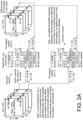
- FIGURE 2A illustrates a schematic block diagram of an exemplary embodiment of multiplier-accumulator circuitry of a plurality of multiplier-accumulator execution pipelines configured in and implementing a concurrent processing techniques, according to certain aspects of the present inventions; notably, in one embodiment, the multiplier-accumulator execution pipelines (in this illustrative embodiment, two pipelines - each pipeline including 64 multiplier-accumulator circuits) are configured to implement a concurrent processing technique may be located in the same cluster of a X1 component (e.g., Cluster A of the X1 component illustrated in FIGURE 1C ) or, in another embodiment, in different clusters of a X1 component (e.g., Clusters A and B of the X1 component illustrated in FIGURE 1C );
- a X1 component e.g., Cluster A of the X1 component illustrated in FIGURE 1C
- FIGURE 1C X1 component
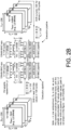
- FIGURE 2B illustrates a schematic block diagram of an exemplary embodiment of multiplier-accumulator circuitry of a plurality of multiplier-accumulator execution pipelines configured in and implementing a concurrent processing techniques, according to certain aspects of the present inventions; notably, in this embodiment, the multiplier-accumulator execution pipelines (in this illustrative embodiment, two pipelines - each pipeline including 64 multiplier-accumulator circuits) are configured in a serial architecture to implement a larger pipeline (in the illustrative embodiment, 2x MAC execution pipeline - here, 128-MAC pipeline having 128 multiplier-accumulator circuits); notably, the serial architecture may be increased or decreased to provide a multiplier-accumulator execution pipeline of a predetermined, desired and/or exact size or "length" (e.g., 2 ⁇ size of multiplier-accumulator execution pipeline s 256); the size or length of the multiplier-accumulator execution pipeline may be configurable or programmable (e.g., one-time or multiple times - such as, in situ (i
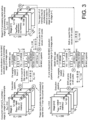
- FIGURE 3 illustrates a schematic block diagram of an exemplary embodiment of a plurality of MAC execution pipelines, configured to process a plurality of stages (e.g., stage [i] and stage [i+1]) of an image plane/frame or planes/frames wherein the execution pipelines process the image data of these stages concurrently (i.e., there is temporal overlap of processing of related data by a plurality of MAC execution pipelines), according to certain aspects of the present inventions; notably, in one embodiment the of MAC execution pipelines are located in the same cluster of pipelines; in another embodiment, the of MAC execution pipelines are located in different clusters of the same X1 component;
- FIGURE 4A illustrates a schematic block diagram of a logical overview of an exemplary embodiment of multiplier-accumulator circuitry of a multiplier-accumulator execution pipeline implementing a filtering data processing technique of the input images/data, according to certain aspects of the present inventions; the configuration and processing technique illustrated in FIGURE 4A may be implemented in any of the concurrent processing techniques and/or configurations/architectures implementing such techniques that are described and/or illustrated herein - including, for example, the embodiments illustrated in FIGURES 2A , 2B and 3 ;
- FIGURE 4B illustrates an exemplary pseudo-code and operation count of the exemplary multiplier-accumulator execution pipeline embodiment illustrated in FIGURE 4A , according to certain aspects of the present inventions;
- FIGURE 5 illustrates a schematic block diagram of a physical overview of an exemplary embodiment of a plurality of multiplier-accumulator execution pipelines, each pipeline including the multiplier-accumulator circuitry (illustrated in block diagram form), wherein the plurality of multiplier-accumulator execution pipelines are configured to implement a Winograd technique of data processing in a concurrent processing configuration/architecture, according to certain aspects of the present inventions; notably, in this example, the 64x(4x4) input pixels/data at dij, which determine the associated 64x(2x2) output pixels at yij, are processed by a plurality (here, 16) of multiplier-accumulator execution pipelines in connection with concurrent operation of multiple execution pipelines of multiple X1 components; see the discussion of the Winograd processing techniques in U.S.
- FIGURE 6A illustrates a high-level block diagram of a plurality of X1 components (e.g., the X1 component illustrated in FIGURE 1C ) disposed on one integrated circuit die, a portion of an integrated circuit die, and/or a printed circuit board or other substrate, according to one or more aspects of the present inventions;
- the plurality of X1 components may be controllable or programmable (e.g., in situ or at start-up/power-up); moreover, the interconnection (e.g., point-to-point or bus such as multi-drop, ring, star, etc.) between the circuitry of the X1 components (e.g., one or more multiplier-accumulator execution pipelines of each X1 component) and/or the operation(s) thereof may be controllable or programmable to, for example, implement coordinated data processing operations, according to one or more aspects of the present inventions; the circuitry of each of the X1 components (e.g., the circuitry of the MAC execution pipeline
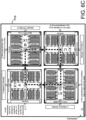
- FIGURE 6B illustrates a high-level block diagram of an integrated circuit including four X1 components (e.g., the X1 component illustrated in FIGURE 1C ) that may be controllably interconnected (e.g., in situ or at start-up/power-up), according to one or more aspects of the present inventions and/or to implement one or more aspects of the present inventions; notably, although FIGURE 6B illustrates four components, these aspects of present inventions are not limited thereto - rather any number of a plurality of components may be controllably interconnected (e.g., the components may be interconnected via a bus interface (e.g., GPIO interface)) and/or the operation(s) thereof controllably coordinated to implement aspects of the present inventions; moreover, the X1 components may or may not be identical in structure, circuitry, architecture and/or configuration; each X1 component, however, includes a plurality of multi-bit MAC execution pipelines having a plurality of multiplier-accumulator circuits each of which implement multiply
- FIGURE 6C illustrates a high-level block diagram of a printed circuit board (PCB) or other substrate including four X1 components (e.g., the X1 component illustrated in FIGURE 1C ) that may be controllably interconnected (e.g., in situ or at start-up/power-up) to implement aspects of the present inventions; notably, although FIGURE 6C illustrates four components, these aspects of present inventions are not limited thereto - rather any number of a plurality of components may be controllably interconnected (e.g., the components may be interconnected via a bus interface (e.g., GPIO interface)) and/or the operation(s) thereof controllably coordinated to implement aspects of the present inventions; moreover, the X1 components may or may not be identical in structure, circuitry, architecture and/or configuration; each X1 component, however, includes a plurality of multi-bit MAC execution pipelines having a plurality of multiplier-accumulator circuits each of which implement multiply and accumulate operations and may be configured according
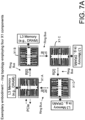
- FIGURE 7A illustrates a high-level block diagram of a plurality of X1 components (in this illustrative exemplary embodiment, 4) wherein the X1 components (e.g., the X1 component illustrated in FIGURE 1C ) is controllably configured/interconnected (e.g., in situ or at start-up/power-up) in a ring topology or architecture to implement certain aspects of the present inventions; here, each of the X1 components is connected to external memory (L3 memory, e.g., DRAM) via interface circuitry and an interface bus; notably, the plurality of components may be configured/interconnected in topologies or architectures other than a ring - all such topologies/architectures are intended to fall within the scope of the present inventions; moreover, the X1 components may or may not be identical in structure, circuitry, architecture and/or configuration; each X1 component, however, includes a plurality of multi-bit MAC execution pipelines having a plurality of multiplier-accumulator
- FIGURE 7B illustrate a schematic block diagram of a logical overview of an exemplary multiplier-accumulator execution pipeline, according to one or more aspects of the present inventions, wherein the multiplier-accumulator execution pipeline includes a plurality of multiplier-accumulator circuitry, which is illustrated in block diagram form, to process data (e.g., image data of a stage of a frame); notably, the multiplier-accumulator circuitry includes one or more of the multiplier-accumulator circuits (although the individual multiplier-accumulator circuits are not specifically illustrated here), for example, a multiplier-accumulator circuit as described and/or illustrated in the exemplary embodiments of FIGURES 1A-1C of the '306 and '345 applications, and the text associated therewith; notably, however, multiplier-accumulator circuits is not limited to the particular circuit, logical, block, functional and/or physical diagrams, block/data width, data path width, bandwidths, and processes illustrated and/or described in accordance with, for example, the exemplary embodiment of FIGURES 1A
- FIGURES 7C to 7E illustrate block diagram representations of a plurality of image frames, each image frame including a plurality of stages, wherein each stage includes a plurality of related image data which is processed, concurrently, via a plurality of X1 components (in this example, four X1 components - see, e.g., FIGURES 6B , 6C and 7A ), according to one or more aspects of the present inventions; in one embodiment, the plurality of multiplier-accumulator execution pipelines of the plurality of X1 components are configured to process the related image data using a configuration or architecture like that of the exemplary embodiment illustrated in FIGURE 7B and the plurality of X1 components are interconnected via a ring bus (see, e.g., FIGURE 7A ); notably, however, the plurality of MAC execution pipelines (each having a plurality of multiplier-accumulator circuits) may be configured to perform multiply and accumulate operations according to any of the aspects of the present inventions including, for example, the processing configurations
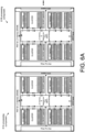
- FIGURE 10 illustrates exemplary data transfer or transport flow between the X1 components in connection with an embodiment implementing 3x3 filtering (e.g., FIGURE 4A ) or implementing Winograd processing technique (e.g., FIGURE 5 ), according to one or more aspects of the present inventions; notably, in each quadrant in each X1 component, one horizontal edge and one vertical edge of input image pixels/data is exchanged with the adjacent X1 component wherein, in one embodiment, this exchange operation may proceed or be implemented in parallel with processing of the interior pixels/data, but this transport delay is completed within the execution time of each quadrant;
- 3x3 filtering e.g., FIGURE 4A
- Winograd processing technique e.g., FIGURE 5
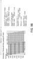
- FIGURE 11A illustrates an exemplary timing diagram of an embodiment of processing wherein each X1 component processes all of the stages of different frames (e.g., FIGURE 7E ), according to one or more aspects of the present inventions; here, the MAC execution/processing pipelines of each component processes all the image pixels of all of the stages in a given frame; notably, the first stage may be input or provided into the associated X1 component (via, for example, an external processor) before the processing of the first stage starts, and the last stage (in this illustrative embodiment, 120th stage) would be communicated, moved or output back to external circuitry (e.g., an external processor or memory) from each of the X1 components;
- external circuitry e.g., an external processor or memory
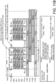
- FIGURE 11B illustrates another exemplary timing diagram of the embodiment of processing wherein each X1 component processes all of the stages of a frame wherein the data of each stage of each frame is processed by a different X1 component (e.g., FIGURE 7E ), according to one or more aspects of the present inventions, wherein the transfer rate (in this illustrative embodiment, 12.5ms) is faster than the transfer rate of the embodiment of FIGURE 11A (in that embodiment, 50ms); here, the MAC execution/processing pipelines of each component processes all the image pixels of all of the stages in a given frame; notably, the first stage may be input or provided into the associated X1 component (via, for example, an external processor) before the processing of the first stage starts, and the last stage (in this illustrative embodiment, 120th stage) would be communicated, moved or output back to external circuitry (e.g., an external processor or memory) from each of the X1 components;
- external circuitry e.g., an external processor or memory
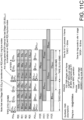
- FIGURE 11C illustrates yet another exemplary timing diagram of the embodiment of processing wherein each X1 component processes all of the stages of a frame wherein the data of each stage of each frame is processed by a different X1 component (e.g., FIGURE 7E ), according to one or more aspects of the present inventions, wherein the transfer rate (in this illustrative embodiment, 16.6ms) is faster than the transfer rate of the embodiment of FIGURE 11A (in that embodiment, 50ms) but slower than the transfer rate of the embodiment of FIGURE 11B (12.5ms); here, the MAC execution/processing pipelines of each component processes all the image pixels of all of the stages in a given frame; notably, the first stage may be input or provided into the associated X1 component (via, for example, an external processor) before the processing of the first stage starts, and the last stage (in this illustrative embodiment, 120th stage) would be communicated, moved or output back to external circuitry (e.g., an external processor or memory) from each of the
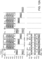
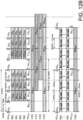
- FIGURES 12A and 12B illustrate exemplary timing diagrams of the embodiment of processing wherein each X1 component processes all of the stages of a frame wherein the data of each stage of each frame is processed by a different X1 component (e.g., FIGURE 7E ) having a transfer rate (50ms) and transfer rate (12.5ms), respectively, according to one or more aspects of the present inventions; and
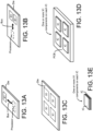
- FIGURES 13A to 13E illustrate, in schematic block diagram form, exemplary embodiments of integrating one or more X1 components into a data processing system, according to one or more aspects of the present inventions; wherein "packaging" or “integration” alternatives, include, for example, (i) fabricating a plurality of X1 components on one or more dice (e.g., FIGURES 13A, 13B and 13C ), (ii) disposing, fixing or placing a plurality of X1 components on a PCB (e.g., FIGURE 13D ), and/or (iii) die-stacking a plurality of X1 components (e.g., FIGURE 13E ); notably, all X1 component packaging and integration architectures, including X1 component communication techniques and/or interconnection architectures (e.g., ring, star or multi-drop bus implementations and/or configurations), are intended to fall within the scope of the present inventions.
- X1 component packaging and integration architectures including X
- the pseudo-code, operations, configurations, block/data width, data path width, bandwidths, data lengths, values, processes and/or algorithms described and/or illustrated in the FIGURES are exemplary and the inventions hereof are not limited to any particular or exemplary circuit, logical, block, functional and/or physical diagrams, number of multiplier-accumulator circuits employed in an execution pipeline, number of execution pipelines employed in a particular processing configuration/architecture, organization/allocation of memory, block/data width, data path width, bandwidths, values, processes, pseudo-code, operations, and/or algorithms illustrated and/or described in accordance with, for example, the exemplary circuit, logical, block, functional and/or physical diagrams.
- the illustrative/exemplary embodiments include a plurality of memories (e.g., L3 memory, L2 memory, L1 memory, L0 memory) which are assigned, allocated and/or used to store certain data and/or in certain organizations, one or more of memories may be added, and/or one or more memories may be omitted and/or combined/consolidated - for example, the L3 memory or L2 memory, and/or the organizations may be changed.
- memories e.g., L3 memory, L2 memory, L1 memory, L0 memory
- the present inventions are directed to one or more integrated circuits having multiplier-accumulator circuitry (and methods of operating such circuitry) including a plurality of multiplier-accumulator execution pipelines that process related data (e.g., image data) concurrently.
- each of the execution pipelines includes a plurality of multiplier-accumulator circuits to perform or implement multiply and accumulate operations in connection with the related data.
- a plurality of separate multiplier-accumulator execution pipelines, each including a plurality of multiplier-accumulator circuits concurrently process related data (e.g., image data).
- the plurality of multiplier-accumulator execution pipelines includes a plurality of registers (including a plurality of shadow registers) that facilitate pipelining of the multiply and accumulate operations to increase throughput of the multiplier-accumulator execution or processing pipelines in connection with processing the related data (e.g., image data such as, e.g., one or more stages of one or more image frames).
- image data such as, e.g., one or more stages of one or more image frames.
- the integrated circuit(s) include a plurality of clusters (e.g., two, four or eight) wherein each cluster includes a plurality of multiplier-accumulator circuit (“MAC") execution pipelines (e.g., 16).
- MAC multiplier-accumulator circuit
- Each MAC execution pipeline may include a plurality of separate multiplier-accumulator circuits (e.g., 64) to implement multiply and accumulate operations.
- a plurality of clusters are interconnected to form a processing component (such component is often identified in the figures as “X1" or “X1 component”) that may include memory (e.g., SRAM, MRAM and/or Flash), a switch interconnect network to interconnect circuitry of the component (e.g., the multiplier-accumulator circuits and/or MAC execution pipeline(s) of the X1 component) and/or circuitry of the component with circuitry of one or more other X1 components.
- the multiplier-accumulator circuits of the one or more MAC execution pipelines of a plurality of clusters of a X1 component may be configured to concurrently process related data (e.g., image data). That is, the plurality of separate multiplier-accumulator circuits of a plurality of MAC execution pipelines may concurrently process related data to, for example, increase the data throughput of the X1 component.
- the X1 component may also include interface circuitry (e.g., PHY and/or GPIO circuitry) to interface with, for example, external memory (e.g., DRAM, MRAM, SRAM and/or Flash memory).
- interface circuitry e.g., PHY and/or GPIO circuitry
- external memory e.g., DRAM, MRAM, SRAM and/or Flash memory.
- the MAC execution pipeline may be any size or length (e.g., 16, 32, 64, 96 or 128 multiplier-accumulator circuits). Indeed, the size or length of the pipeline may be configurable or programmable (e.g., one-time or multiple times - such as, in situ (i.e., during operation of the integrated circuit) and/or at or during power-up, start-up, initialization, re-initialization, configuration, re-configuration or the like).
- the one or more integrated circuits include a plurality of components or X1 components (e.g., 2, 4, ...), wherein each component includes a plurality of the clusters having a plurality of MAC execution pipelines.
- one integrated circuit includes a plurality of components or X1 components (e.g., 4 clusters) wherein each cluster includes a plurality of execution or processing pipelines (e.g., 16, 32 or 64) which may be configured or programmed to process, function and/or operate concurrently to process related data (e.g., image data) concurrently.
- the related data is processed by each of the execution pipelines of a plurality of the clusters concurrently to, for example, decrease the processing time of the related data and/or increase data throughput of the X1 components.
- a plurality of execution or processing pipelines of each of the clusters of a plurality of the X1 components may be interconnected, for example, in a ring configuration or architecture to concurrently process related data (e.g., image data).
- a plurality of MAC execution pipelines of one or more (or all) of the clusters of a plurality of X1 components may be interconnected in a ring configuration or architecture (wherein a bus interconnects the components) to concurrently process related data.
- a plurality of MAC execution pipelines of one or more (or all) of the clusters of each X1 component are configured to process one or more stages of an image frame such that circuitry of each X1 component processes one or more stages of each image frame of a plurality of image frames.
- a plurality of MAC execution pipelines of one or more (or all) of the clusters of each X1 component are configured to process one or more portions of each stage of each image frame such that circuitry of each X1 component is configured to process a portion of each stage of each image frame of a plurality of image frames.
- a plurality of MAC execution pipelines of one or more (or all) of the clusters of each X1 component are configured to process all of the stages of at least one entire image frame such that circuitry of each X1 component is configured to process all of the stage of at least one image frame.
- each X1 component is configured to process all of the stages of one or more image frames such that the circuitry of each X1 component processes a different image frame.
- the multiplier-accumulator circuitry in the execution pipeline operates concurrently.
- "r" e.g., 64 in the illustrative embodiment
- MAC processing circuits in the execution pipeline operate concurrently whereby the multiplier-accumulator processing circuits perform r ⁇ r (e.g., 64x64) multiply-accumulate operations in each r (e.g., 64) cycle interval (here, a cycle may be nominally 1ns).
- r e.g., 64 in the illustrative embodiment
- MAC processing circuits in the execution pipeline operate concurrently whereby the multiplier-accumulator processing circuits perform r ⁇ r (e.g., 64x64) multiply-accumulate operations in each r (e.g., 64) cycle interval (here, a cycle may be nominally 1ns).
- next input pixels/data e.g., 64
- the previous output pixels/data are shifted-out during the same r (e.g., 64) cycle interval.
- each r (e.g., 64) cycle interval processes a Dd/Yd (depth) column of input and output pixels/data at a particular (i,j) location (the indexes for the width Dw/Yw and height Dh/Yh dimensions).
- the r (e.g., 64) cycle execution interval is repeated for each of the Dw*Dh depth columns for this stage.
- the filter weights or weight data are loaded into memory (e.g., the L1/L0 SRAM memories) from, for example, an external memory or processor before the stage processing started (see, e.g., the '306 provisional application).
- the method implemented by the configuration illustrated may accommodate arbitrary image/data plane dimensions (Dw/Yw and Dh/Yh) by simply adjusting the number of iterations of the basic 64x64 MAC accumulation operation that are performed.
- the loop indices "I” and "j" are adjusted by control and sequencing logic circuitry to implement the dimensions of the image/data plane.
- the method may also be adjusted and/or extended to handle a Yd column depth larger than the number of MAC processing elements (e.g., 64 in this illustrative example) in the execution pipeline. In one embodiment, this may be implemented by dividing the depth column of output pixels into blocks of 64, and repeating the 64x64 MAC accumulation of FIGURE 1A for each of these blocks.
- the method illustrated in FIGURE 1A may be further extended to handle a Dd column depth larger than the number of MAC processing elements (64 in this illustrative example) in the execution pipeline.
- This may be implemented, in one embodiment, by initially performing a partial accumulation of a first block of 64 data of the input pixels Dijk into each output pixel Yijl'. Thereafter, the partial accumulation values Yijl' are read (from the memory Y mem ) back into the execution pipeline as initial values for a continuing accumulation of the next block of 64 input pixels Dijk into each output pixel Yijl.
- the memory which stores or holds the continuing accumulation values (e.g., L2 memory) may be organized, partitioned and/or sized to accommodate any extra read/write bandwidth to support the processing operation.
- the pseudo-code illustrated in FIGURE 1B illustrates the looping performed by the control and sequencing logic associated with the MAC execution pipeline.
- This looping shows the accumulation of the products of Dijk input pixels and Fkl filter values into partial sums Yijl.
- the partial sums Yijl are then accumulated into the final output pixel values Yijl.
- the output pixel values/data may thereafter be stored in memory (e.g., L2 memory) and/or provided to external circuitry for processing and/or analysis.
- circuitry and techniques which generalize the applicability of the 64x64 MAC execution pipeline, may also be utilized or extend the generality of the additional processing methods or techniques that will be implemented or described in later sections of this application.
- the integrated circuit may include a plurality of multi-bit MAC execution pipelines which are organized as one or more clusters of a processing component.
- the component may include "resources" such as a bus interfaces (e.g., a PHY and/or GPIO) to facilitate communication with circuitry external to the component and memory (e.g., SRAM and DRAM) for storage and use by the circuitry of the component.
- resources such as a bus interfaces (e.g., a PHY and/or GPIO) to facilitate communication with circuitry external to the component and memory (e.g., SRAM and DRAM) for storage and use by the circuitry of the component.
- X1 the component
- each cluster includes a plurality of multi-bit MAC execution pipelines (in this illustrative embodiment 16 64-MAC execution pipelines).
- a single 64-MAC execution pipeline of FIGURE 1A is illustrated at the lower right for reference purposes.
- the memory hierarchy in this exemplary embodiment includes an L0 memory (e.g., SRAM) that stored filter weights or coefficients to be employed by multiplier-accumulator circuits in connection with the multiplication operations implemented thereby.
- each MAC execution pipeline includes an L0 memory to store the filter weights or coefficients associated with the data under processing by the circuitry of the MAC execution pipeline.
- An L1 memory (a larger SRAM resource) is associated with each cluster of MAC execution pipelines. These two memories may store, retain and/or hold the filter weight values Fijklm employed in the accumulation operations.
- FIGURE 1C may employ an L2 memory (e.g., an SRAM memory that is larger than the SRAM of L1 or L4 memory).
- the X1 component may connect to an external memory (e.g., an even larger external L3 DRAM) that may be shared by one or more (or all) of the clusters of MAC execution pipelines.
- These memories store or hold the input image pixels Dijk and the output image pixels Yijl, as well as filter weight values Fijklm.
- L3 memory e.g., L3 memory, L2 memory, L1 memory, L0 memory
- memories e.g., L3 memory, L2 memory, L1 memory, L0 memory
- one or more of other memories may be added, and/or one or more memories may be omitted and/or combined/consolidated - for example, the L3 memory or L2 memory, and/or the organizations may be changed. All combinations are intended to fall within the scope of the present inventions.
- multiplier-accumulator circuitry and/or multiplier-accumulator pipeline is, at times, labeled "NMAX”, “NMAX pipeline”, “MAC”, or "MAC pipeline”.
- a plurality of multiplier-accumulator execution pipelines concurrently processes related data (e.g., image data).
- each of the execution pipelines includes a plurality of multiplier-accumulator circuits to perform or implement multiply and accumulate operations in connection with the related data.
- the processing (e.g., multiply and accumulate operations) of the related data by the circuits of a plurality of separate multiplier-accumulator execution pipelines is temporally concurrent.
- the plurality of multiplier-accumulator execution pipelines includes a plurality of registers (not illustrated) that facilitate pipelining of the multiply and accumulate operations to increase throughput of the multiplier-accumulator execution or processing pipelines in connection with processing the related data.
- two or more MAC execution pipelines concurrently process the related data.
- the multiply and accumulate operations by the multiplier-accumulator circuits of the execution pipelines are performed or implemented in parallel.
- the stage may utilize additional 64-MAC execution pipelines in parallel to operate concurrently on other pixels/data (i',j') of the input frame or data layers.
- This may utilize additional L2 memory ports (e.g., by dividing, segmenting or splitting the L2 memory across multiple physical SRAM blocks).
- the concurrent MAC execution pipeline operation duplicates the weight data (labeled as Fkl) across the memory (e.g., L0 memory) so that the multiplier-accumulator circuits of each MAC execution pipeline may operate in parallel or concurrently.
- the MAC execution pipelines (and circuitry thereof) of the embodiment illustrated in FIGURE 2A may be located (i) within the same cluster (of 16 pipelines in this illustrative embodiment) and/or (ii) within another cluster of the same X1 processing component
- the MAC execution pipelines may be made deeper by connecting the associated shifting chains in series whereby the multiply and accumulate operations are implemented concurrently with respect to related data.
- two or more MAC execution pipelines are configured as serial execution pipelines to concurrently process data.
- the stage includes an input depth and an output depth which are equal or greater than 2*64 (i.e., greater than 2 time the size of the MAC execution pipeline).
- two 64-MAC execution pipelines are connected serially to form a 128-MAC execution pipeline.
- the 128 MAC processing elements/circuits in this pipeline configuration operate concurrently.
- the 128 cycle execution interval is repeated twice for each of the Dw*Dh depth columns for this stage (conv16 in this example).
- the filter weights were loaded into the memory (e.g., L1/L0 SRAM memories) before the stage processing started (see, e.g., the '306 and '345 applications).
- Dd 256.
- the MAC execution pipelines of the embodiment illustrated in FIGURE 2B may be located (i) within the same cluster (of 16 pipelines in this illustrative embodiment) and/or (ii) within another cluster of the same X1 processing component.
- multiplier-accumulator circuitry of a plurality of MAC execution pipelines implement or perform multiply and accumulate operations concurrently in connection with related image data of a plurality of stages of a frame.
- a plurality of multiplier-accumulator circuits of a first MAC execution pipeline process image data of a first stage (i.e., stage [i]) of a given frame.
- the processed data corresponding to stage [i] is stored in memory Y MEM (e.g., L2 memory - such as SRAM).
- a plurality of multiplier-accumulator circuits of a second MAC execution pipeline starts processing image data corresponding to a second stage (i.e., stage [i+1]).
- the data corresponding to the second stage i.e., stage [i+1]
- stage [i+1] is stored in memory Y MEM /D MEM .
- the region of the memory e.g., L2 memory
- stage [i] and stage [i+1] temporally overlap such that the MAC execution pipeline processes data of the stage [i+1] starts before the MAC execution pipeline finishes processing data of stage [i]. That is, the two MAC execution pipelines process the related data concurrently given that the data of stage [i] relates to the data of stage [i+1] - here, data of different stages of same image frame.
- the data of stage [i+1], as processed by the circuitry of the second MAC execution pipeline, is stored in memory Y MEM (e.g., L2 memory) as stage [i+2].
- This temporal overlapping may provide a performance advantage in the form of reduced processing time, as with the configurations and processing techniques described/illustrated in the embodiments of FIGURES 1 , 2A and 2B . That is, in the exemplary embodiments illustrated in FIGURES 1 , 2A and 2B , the input pixels/data (i.e., Dw*Dh*Dd) of a given stage may be completely processed into the output pixels of the next stage before the starting the processing of data associated with that/successive next stage.
- each depth column Dijk of input pixels/data may be largely independent of other depth columns in the Dw and Dh dimensions. In this way, each depth column may be used and overwritten with a depth column from the next stage, thereby reducing the total memory (e.g., L2 memory) employed in the processing of each stage. Note that there may be a small dependency between adjacent depth columns with filter sizes larger than 1x1 (3x3, the most common larger size is an example of this).
- the memory footprint/allocation of each stage represents a partial subset of the full stage, represented as a highlighted strip on the right side of each of the Dw*Dh planes. Depth columns of input pixels are processed from stage [i] and written into output pixels of stage [i+1] at time T1.
- control and sequencing logic transfers, communicates or moves to a different part of the input strip for stage [i] for the stage[i] to stage[i+1] processing.
- the control and sequencing logic for the second MAC execution pipeline may concurrently (at time T2) begin processing the stage [i+1] pixels/data into stage [i+2] pixels/data.
- the time lag (T2-T1) may provide a margin for managing the two concurrent processes.
- the MAC execution pipelines of the embodiment illustrated in FIGURE 3 may be located (i) within the same cluster (of 16 pipelines in this illustrative embodiment) and/or (ii) within another cluster of the same X1 processing component.
- the embodiment may include more than two MAC execution pipelines - e.g., the method illustrated in FIGURE 3 may be extended with a third MAC execution pipeline processing the stage [i+2] image data into stage [i+3] image data.
- additional MAC execution pipelines may also be employed to extend the larger processing pipeline further.
- the memory may also need to accommodate the adjacent pixel dependency for the case of 3x3 (and higher order) filtering for a stage.
- FIGURE 4A illustrates an exemplary embodiment of a concurrent operation of the NMAX execution pipeline (having the MAC processing elements (in this exemplary embodiment, 64)) concurrently operate the MAC execution pipelines with filtering of the input images/data (e.g., 3x3), according to certain aspects of the present inventions.
- each MAC execution pipeline performs 9x64x64 MAC (multiply-accumulate) operations in each 9x64 cycle interval (a cycle is nominally 1ns).
- each of 9 sets of 64 input pixels/data are shifted-in during one 64-cycle interval.
- the previous 64 output pixels are shifted-out during a single 64 cycle interval.
- Each 9x64 cycle interval processes a Dd/Yd (depth) column of input pixels/data at a particular (i,j) location (the indexes for the width Dw/Yw and height Dh/Yh dimensions).
- Each 9x64 cycle interval produces a half-depth (64) of output pixels.
- the 9x64 cycle execution interval is repeated twice for each of the Yw*Yh depth columns for this stage (conv10 in this example).
- the filter weights or data may be loaded into memory (e.g., the L1/L0 SRAM memories) before stage processing is started.
- the pseudo-code illustrated in FIGURE 4B is similar to the code illustrated in FIGURE 1B , with the exception of the inner loop wherein an index "m" has been added.
- the loop of FIGURE 4B provides/illustrates the accumulation of the products Uijklm of Dijkm input pixels/data and Fklm filter values into temporary sums Vijkl. The temporary sums Vijkl are then accumulated into the final output pixel/data values Yijl.
- the two accumulation loops of the pseudo-code illustrated in FIGURE 4B may be implemented in alternate, equivalent orders (i.e. the order of the "m” and "k” loops).
- the concurrent operations implementing a filtering of the input images/data as set forth in the exemplary embodiment of FIGURE 4A may include or implement pipelined concurrent processing techniques (see
- FIGURE 1A parallel concurrent processing techniques
- FIGURE 2A serial concurrent processing techniques
- FIGURES 2B overlap concurrent processing techniques
- FIGURE 3 overlap concurrent processing techniques
- FIGURE 5 illustrates an exemplary embodiment of concurrent processing technique, based on Winograd type processing, employing multiplier-accumulator circuits of one or more MAC execution pipelines having conversion logic implement Winograd type processes, according to certain aspects of the present inventions.
- each MAC pipeline handles one word of all of the (e.g., 16) words (m) in each dij group during each group interval (e.g., 64ns).
- the architecture of FIGURE 5 implements processing that is functional equivalent to that illustrated in FIGURE 4 .
- the MAC pipelines perform 16x64x64 MAC operations in a 64 cycle interval (16/9 more than method FIGURE 4 ), but produces more 256 output pixels in this interval (four times more than the 64 pixels of the method illustrated in FIGURE 4 ) - as described in the '111 and '161 applications.
- the concurrent operations implementing Winograd type processing in connection with the input images/data may include or implement pipelined concurrent processing techniques (see FIGURE 1A ), parallel concurrent processing techniques (see FIGURE 2A ), serial concurrent processing techniques ( FIGURE 2B ), or overlap concurrent processing techniques (see FIGURE 3 ); all combinations and permutations are intended to fall within the scope of the present inventions.
- the MAC execution pipelines of the X1 component(s) may implement the Winograd processing via any of the architectures or configurations set forth in the exemplary embodiments of FIGURES 1A , 2A , 2B , 3 , 4A and 7B .
- the MAC execution pipelines may be located (i) within the same cluster (of 16 pipelines in this illustrative embodiment) and/or (ii) within another cluster of the same X1 processing component.
- the one or more integrated circuits may include a plurality of components (e.g., 2, 4, ...), wherein each component includes a plurality of clusters and each cluster includes a plurality of MAC execution pipelines (e.g., 16).
- one integrated circuit includes a plurality of components or X1 components (e.g., 4 clusters) wherein each cluster includes a plurality of execution or processing pipelines (e.g., 16, 32 or 64) which are configured to process, function and/or operate concurrently such that related data is processed by each of the execution pipelines of a plurality of the clusters concurrently to, for example, decrease the processing time of the related data and/or increase data throughput of the X1 components,
- a plurality of execution or processing pipelines of each of the clusters of a plurality of the X1 components may be interconnected, for example, in a ring configuration or architecture, via a ring bus, to concurrently process related data (e.g., image data).
- a plurality of MAC execution pipelines of one or more (or all) of the clusters of a plurality of X1 components may be interconnected in a ring configuration or architecture to concurrently process related data.
- a plurality of MAC execution pipelines of one or more (or all) of the clusters of each X1 component are configured to process one or more stages of an image frame such that circuitry of each X1 component processes one or more stages of each image frame of a plurality of image frames.
- a plurality of MAC execution pipelines of one or more (or all) of the clusters of each X1 component are configured to process one or more portions of each stage of each image frame such that circuitry of a plurality of X1 component are configured to process only a portion of each stage of each image frame of a plurality of image frames - wherein together the processing components process all of the stages of the entire image frame.
- a plurality of MAC execution pipelines of one or more (or all) of the clusters of each X1 component is configured to process all of the stages of an entire image frame.
- the circuitry of MAC execution pipelines of each X1 component process a different image frame of the plurality of image frames.
- a plurality (or all) of the execution or processing MAC pipelines of each of the clusters of each of the components may be configured to function or operate and/or process image data concurrently, including, for example, those configurations set forth in the exemplary embodiments of FIGURES 2A , 2B and/or 3.
- the components including a plurality (or all) of execution or processing pipelines of the clusters of each processing component
- the plurality of components may share resources, for example, (i) one or more bus interfaces (e.g., a PHY and/or GPIO) to facilitate communication with circuitry external to the plurality of component and/or (ii) memory (e.g., SRAM and DRAM) for storage and use by the circuitry of the components during, for example, operation of the MAC processing pipelines.
- bus interfaces e.g., a PHY and/or GPIO
- memory e.g., SRAM and DRAM
- a plurality of the processing components may be disposed on separate die and/or on the same die - all combinations are intended to call within the scope of the present inventions.
- the components may be disposed on a printed circuit board (PCB) and/or organized in a stacked die configuration.
- PCB printed circuit board
- the plurality/multiple of X1 components may be integrated or incorporated into a system via several "packaging” or “integration” alternatives. Such alternatives provide a range of wiring connections, which may provide guidance for the external signaling bandwidth.
- [1] FR4/PCB (printed circuit board) substrate with BGA (ball grid array) packaged devices typically 300-1000u substrate wire pitch
- [2] silicon substrate (or equivalent) with C4 packaged silicon die directly attached typically 100-300u substrate wire pitch
- [3] package-stacked devices typically with wire-bonded connection between silicon die stacked together in a package (typically 50u-200u wire pitches)
- [4] die-stacked devices with silicon die stacked and connected with vertical through-die vias in a package (typically 10u-50u wire pitches.
- processing components are often depicted for illustrative purposes as identical (see FIGURES 6A-6C ) - although it should be noted the processing components may be different (e.g., include different external interface circuitry). Moreover, in many of the embodiments, the processing system includes four processing components - although more or less processing components may be employed (e.g., 2, 3, 5, 6, etc.). As noted above, such processing components are often referred to in the text and identified in the figures as "X1 component" or "X1".
- the processing system may include a plurality of processing or X1 components, each component including a plurality of multi-bit MAC execution pipelines having a plurality of multiplier-accumulator circuits each of which implement multiply and accumulate operations.
- the MAC execution pipelines and/or the plurality of multiplier-accumulator circuits may be configured to implement one or more processing architectures or techniques (singly or in combination with one or more X1 components).
- the MAC execution pipelines are organized into clusters (in this illustrative embodiment, four clusters wherein each cluster includes a plurality of multi-bit MAC execution pipelines (in this illustrative embodiment each cluster includes 16, 64-MAC execution pipelines)).
- the plurality of multiplier-accumulator circuitry are configurable or programmable (one-time or multiple times, e.g., at start-up and/or in situ) to implement one or more pipelining processing architectures or techniques (see, e.g., the expanded view of a portion of the high-level block diagram of FIGURE 1C in the lower right is a single 64-MAC execution pipeline illustrated in FIGURE 1A ).
- the X1 components in this illustrative embodiment may include memory (e.g., L2 memory, L1 memory and L0 memory (e.g., SRAM)), a bus interfaces (e.g., a PHY and/or GPIO) to facilitate communication with circuitry external to the component and memory (e.g., SRAM and DRAM) for storage and use by the circuitry of the component, and a plurality of switches/multiplexers which are electrically interconnected to form a switch interconnect network "Network-on-Chip" (“NOC”) to facilitate interconnecting the clusters of multiplier-accumulator circuits of the MAC execution pipelines.
- memory e.g., L2 memory, L1 memory and L0 memory (e.g., SRAM)
- bus interfaces e.g., a PHY and/or GPIO
- switches/multiplexers which are electrically interconnected to form a switch interconnect network "Network-on-Chip" (“NOC”) to facilitate interconnecting the cluster
- the NOC includes a switch interconnect network (e.g., a mixed-mode interconnect network (i.e., a hierarchical switch matrix interconnect network and a mesh, torus or the like interconnect network (hereinafter collectively “mesh network” or “mesh interconnect network”)), associated data storage elements, input pins and/or look-up tables (LUTs) that, when programmed, determine the operation of the switches/multiplexers.
- a switch interconnect network e.g., a mixed-mode interconnect network (i.e., a hierarchical switch matrix interconnect network and a mesh, torus or the like interconnect network (hereinafter collectively “mesh network” or “mesh interconnect network”)
- messages network i.e., a hierarchical switch matrix interconnect network and a mesh, torus or the like interconnect network (hereinafter collectively “mesh network” or “mesh interconnect network”)
- LUTs look-up tables
- one or more (or all) of the clusters
- each MAC execution pipeline has dedicated L0 memory (e.g., SRAM memory), and a plurality (e.g., 16) MAC execution pipelines of a MAC cluster share L1 memory (e.g., SRAM memory).
- L0 memory e.g., SRAM memory
- a plurality (e.g., 16) MAC execution pipelines of a MAC cluster share L1 memory (e.g., SRAM memory).
- the NOC may couple to the L2 memory to the PHY (physical interface) which may connect to L3 memory (e.g., external DRAM).
- the NOC may also couple to a PCIe or PHY which, in turn, may provide interconnection to or communication with circuitry external to the X1 component (e.g., another X1 component and/or an external processor, such as a host processor).
- the NOC may also connect a plurality of X1 components (e.g., via GPIO input/output PHYs) which allow multiple X1 components to process related data (e.g., image data) concurrently, as discussed herein.
- X1 components e.g., via GPIO input/output PHYs
- related data e.g., image data
- the plurality of X1 components may be disposed on an integrated circuit die, a portion of an integrated circuit die, and/or a printed circuit board or other substrate.
- the plurality of X1 components may be controllable or programmable (e.g., in situ or at start-up/power-up).
- the interconnection e.g., point-to-point or bus such as multi-drop, ring, star, etc.
- the circuitry of the X1 components, and/or the operation(s) thereof may be controllable or programmable to, for example, implement coordinated data processing operations.
- each of the X1 components may be configurable or programmable (e.g., one-time or multiple times - such as, in situ (i.e., during operation of the integrated circuit) and/or at or during power-up, start-up, initialization, re-initialization, configuration, re-configuration or the like).
- the X1 components may or may not be identical in structure, circuitry, architecture and/or configuration.
- Each X1 component includes a plurality of multi-bit MAC execution pipelines having a plurality of multiplier-accumulator circuits each of which implement multiply and accumulate operations.
- the processing components may be interconnected via a bus interface (e.g., GPIO interface).
- a bus interface e.g., GPIO interface
- the components are connected in a ring (see the dashed lines disposed over the components (which are identified as "X1", “X1A”, “X1B”, “X1C” and “X1D”).
- the ring topology is employed for illustrative purposes here because, for example, it is symmetric, and the links are point-to-point and unidirectional.
- the present inventions may employ other architectures, topologies and connection methods are suitable - all of which are intended to fall within the scope of the present inventions.
- a star topology or multi-drop bus topology may be employed to interconnect a plurality of components.
- the interconnection conductors or links may be unidirectional or bidirectional.
- the impact on the performance of the processing system may be the signaling bandwidth of the individual links between the X1 components.
- the choice of how to manage or control these links may have less impact, and alternatives to the ring topology are available and may be more suitable or advantageous when considering other criteria or factors.
- each bus interface is unidirectional with a plurality e.g., 16) conductors/wires and clock/control, and operating at a common signaling rate (e.g., 150Mb/s).
- a common signaling rate e.g. 150Mb/s.
- This provides a transport bandwidth between the individual X1 components (whether disposed on a common die or on a PCB).
- other interconnection architectures or designs may be employed, which may increase the bandwidth by 10-30x, allowing much higher performance levels.
- all architectures, topologies, designs and communication techniques to connect a plurality of X1 components are intended to fall within the scope of the present inventions.
- only one of the X1 components is connected directly to the interface that provides connection to circuitry external to the components (e.g., a PCIe interface of, for example, the PCB).
- the number of interfaces for example, PCIe interfaces
- Such external circuitry e.g., a processor or controller
- Such a configuration may provide sufficient bandwidth to move pixel/image data between, for example, a processor and the plurality of components - wherein the "bottleneck" in the configuration will likely generally be the communication of data via the ring bus.
- the system including a plurality of processing components may be configured to implement concurrently processing of a plurality of images frames, each image frame including a plurality of stages, wherein each stage includes a plurality of related image data.
- a plurality of related image data is processed concurrently via a plurality of multiplier-accumulator execution pipelines of the plurality of X1 components (see FIGURE 7B ) wherein the plurality of X1 components are interconnected via a ring bus (see, e.g., FIGURE 7A ).
- a plurality of MAC execution pipelines in each of the X1 components processes a plurality of different stages of an image frame.
- each group of stages of each frame is processed by a plurality of MAC execution pipelines of one or more (or all) of the clusters of different X1 component.
- each group of stages is processed by a plurality of MAC execution pipelines of one or more (or all) of the clusters of a different processing components X1A. X1B, X1C and X1D.
- Stage 000 to Stage 029 is processed by component X1A
- Stage 030 to Stage 059 is processed by component X1B
- Stage 060 to Stage 089 is processed by component X1D
- Stage 090 to Stage 119 is processed by component X1C).
- the processing of each group of stages of each frame may be concurrent relative to the processing of other groups of stages of each frame.
- a plurality of MAC execution pipelines of one or more (or all) of the clusters of each X1 component are configured to process a portion of each stage of each image frame such that circuitry of a plurality of X1 component are configured to process only a portion of each stage - wherein taken together the processing components process all of the stages of the entire image frame.
- each stage is processed by a plurality of MAC execution pipelines of one or more (or all) of the clusters of processing components X1A, X1B, X1C and X1D. (See Inset A).
- the processing of each portion of each stage may be concurrent relative to the processing of other portions of the associated stage.
- a plurality of MAC execution pipelines of one X1 component is configured to process all of the stages of an entire image frame. See, e.g., FIGURE 7E ).
- the circuitry of MAC execution pipelines of each X1 component process a different image frame of the plurality of image frames.
- the processing of the frames may be concurrent - that is, MAC execution pipelines of each X1 component may process the data of each stage concurrently with respect to the processing of other frames by the other X1 components of the system.
- a plurality of execution or processing pipelines of each of the clusters of a plurality of the X1 components may be interconnected, for example, in a ring configuration or architecture to facilitate concurrently process related data (e.g., image data).
- the processing pipelines of each X1 component may be configured to implement the processing technique as illustrated in FIGURE 7B or FIGURE 1A .
- the processing pipelines of each X1 component may be configured, for example, in a parallel concurrent processing configuration (see, e.g., FIGURE 2A ), a serial concurrent processing configuration (see, e.g., FIGURES 2B ), or overlap concurrent processing configuration (see, e.g., FIGURE 3 ).
- the MAC execution or processing pipelines (each having a plurality of multiplier-accumulator circuits) of the X1 components may be configured, for example, as illustrated in FIGURES 4A and 5 to implement the filtering operations; all combinations and permutations are intended to fall within the scope of the present inventions.
- the configuration(s) of the processing pipelines employed in each X1 component may be the same or different within each X1 component as well as between X1 components; again, all combinations and permutations are intended to fall within the scope of the present inventions.
- CNN convolutional neural network
- This synthetic benchmark assumes there are 120 stages per frame (YOLOv3 has 106), each stage requires 1.66 ⁇ 2 ⁇ 30 MAC operations per stage (YOLOv3 has an average of about 1.4 ⁇ 2 ⁇ 30 in embodiments implementing Winograd type processing techniques), and each stage has an input image and an output image that are both 16MB in size (most of the YOLOv3 frames are 2, 4, 8, or 16MB in size).
- the uniform structure of the synthetic CNN makes it easier to analyze the architectural performance of the concurrent execution methods.
- each X1 component has 4K MAC execution elements, with each performing one MAC operation per nanosecond, and the ring bandwidth is 300MB/s for the initial analysis.
- the time for one X1 component to process 120 stages of one image frame is tEXEC ⁇ 50ms
- the time for the ring bus to transfer one stage of image data (16MB) across one ring link is tXFER - 50ms.
- FIGURES 7A-7C an exemplary embodiment of a method of processing wherein a stack of image frames ( FIGURE 7C ) represent the amount of "work" to be done (i.e., data to be processed).
- the stages are divided between the four X1 components, with each component processing 30 stages before communicating, outputting and/or passing the data of the final stage to the next X1 component for the next 30 stages. This process continues until the data of the final stage is communicated, output and/or passed back to the X1 with the bus interface (e.g., PCIe interface) that connects to external circuitry (e.g., processor).
- the bus interface e.g., PCIe interface
- FIGURES 7A , and 7D illustrate an exemplary embodiment of processing wherein each of stage (e.g., 120 stages) of each frame is divided into sections (in this example, four - one for each of X1 components - using the Dw and Dh dimensions).
- stage e.g., 120 stages
- sections in this example, four - one for each of X1 components - using the Dw and Dh dimensions.
- one or more (or all) of the processing pipelines of each X1 component processes the image pixels/data corresponding to its section of the stage.
- pixels/data at the boundary may be shared for layers that perform 3x3 filtering operations.
- the first stage may be input or provided into the four X1 components (via, for example, an external processor) before processing of the first stage starts, and the last (120th) stage would be communicated, moved or output back to external circuitry (e.g., an external processor or memory) from the X1 components.
- external circuitry e.g., an external processor or memory
- FIGURES 7A and 7E illustrate an exemplary embodiment of processing wherein each frame (with 120 stages) is allocated for processing by a different X1 component.
- the MAC execution or processing pipelines of each component process all the image pixels of all stages in the frame.
- FIGURE 7B illustrates an exemplary configurations of the MAC execution pipelines of the X1 component(s); although other configurations of the MAC execution pipelines of the X1 component(s) may be employed - including, e.g., architectures or configurations set forth in the exemplary embodiments of FIGURES 1A , 2A , 2B , 3 , 4A and 5 ).
- the first stage may be input or provided into the associated X1 component (via, for example, an external processor) before the processing of the first stage starts, and the last (120th) stage would be communicated, moved or output back to external circuitry (e.g., an external processor or memory) from each of the X1 components.
- external circuitry e.g., an external processor or memory
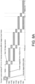
- FIGURE 8A illustrates an exemplary timing diagram of the embodiment of processing the image pixels/data of FIGURE 7C (i.e., wherein X1 component (having a plurality of clusters and each cluster includes a plurality of MAC execution pipelines - see, e.g., the configuration of FIGURES 7A and 7B )) processes all 30 stages before communicating, writing and/or sending the final output stage to the next X1 component.
- X1 component having a plurality of clusters and each cluster includes a plurality of MAC execution pipelines - see, e.g., the configuration of FIGURES 7A and 7B )
- the stages are divided between the four X1 components, with plurality of MAC execution pipelines of each component processing stages before communicating, outputting, transferring and/or passing the data of the final stage to the next X1 component for processing of the next stages.
- each X1 component uses 12.5ms for its 30 stage execution pipeline to process the data, and 50ms to transfer and/or output the pixel/data of the last stage to the execution pipelines of the next X1 component. This is repeated four times - for each of the components of the system/architecture - for a total of 250ms of batch 1 latency. Notably, 50ms of this process is execution time and 200ms is data transfer or transport time.
- the performance here may be better, since four frames can be processed in the same 250ms interval. In fact, with a small amount of buffering at the ring bus interfaces, five frames may be processed in 250ms, making the concurrent batch5 performance of the four X1 components equal to four times the single X1 performance with a ring bus of very moderate bandwidth.
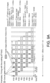
- FIGURE 8B illustrates an exemplary timing diagram of the embodiment of processing the image pixels/data of FIGURE 7B (i.e., wherein each X1 component (having a plurality of clusters and each cluster includes a plurality of MAC execution pipelines - see, e.g., the configuration of FIGURES 7A and 7C )) processes 1/4th of all stages before sending 1/4th of the final output stage to the next X1 component.
- each X1 component uses 12.5ms for each 1/4th of the 30 stage execution pipeline, and 12.5ms to transfer 1/4th of the last stage to the next X1 component. This process is repeated four times.
- this embodiment may employ the MAC execution pipeline configuration of FIGURE 7B ; although other MAC execution pipeline configurations may be implemented - including, for example, an overlapping processing technique and configuration in relation to its operations with the processing operations performed in the next X1 component. (See, e.g., FIGURE 3 ).
- FIGURE 8C illustrates an exemplary timing for a case in which an X1 component processes 1/16th of all 30 stages before sending 1/16th of the final output stage to the next X1 component (see, e.g., the configuration of FIGURES 7A , 7B and 7D ).
- each X1 component uses 3.125ms for each 1/16th of the 30 stage execution pipeline, and 3.125ms to transfer 1/16th of the last stage to the next X1 component. This process is repeated 16 times.
- this embodiment may employ the MAC execution pipeline configuration of FIGURE 7B ; although other pipeline configurations may be implemented - including, for example, an overlapping processing technique and configuration in relation to its operations with the processing operations performed in the next X1 component. (See, e.g., FIGURE 3 ).
- each X1 component uses 3.125ms for each 1/16 th of the 30 stage execution pipeline, and 3.125ms to transfer 1/16 th of the last stage to the next X1 component.
- FIGURE 10 illustrates an embodiment of processing method segments, divides and/or splits the processing of each stage between the four of the X1 components.
- each set of input pixels/data at an (i,j) position (in the Dw,Dh planes) is converted into a set of output pixels/data at the (i,j) position (in the Yw,Yh planes) before processing is completed at that position for the next stage.
- the pixels/data at each (i,j) position are independent (except for adjacent positions for 3x3 filtering), so that, in one embodiment, concurrent processing or operations in the four quadrants of the stage may be implemented. That is, the processing pipelines of each X1 component may be configured, for example, in a parallel concurrent processing configuration (see, e.g., FIGURE 2A ), a serial concurrent processing configuration (see, e.g., FIGURES 2B ), or overlap concurrent processing configuration (see, e.g., FIGURE 3 ).
- the MAC execution or processing pipelines (each having a plurality of multiplier-accumulator circuits) of the X1 components may be configured, for example, as illustrated in FIGURES 4A and 5 to implement the filtering operations; all combinations and permutations are intended to fall within the scope of the present inventions. Indeed, the configuration(s) of the processing pipelines employed in each X1 component may be the same or different within each X1 component as well as between X1 components.
- Transfer or transport overhead between the X1 components may be considered for the situation where 3x3 filtering is employed. This case is shown in FIGURE 10 , with the added assumption of implementing Winograd processing techniques/circuitry.
- each quadrant in each X1 component one horizontal edge and one vertical edge of input image pixels/data is exchanged with the adjacent X1 component. This exchange operation may proceed in parallel with processing of the interior pixels/data, but this transport delay is completed within the execution time of each quadrant.
- the execution time will be 0.1ms/stage for the synthetic CNN, and the exchange delay per stage will be approximately 0.1ms (2 ⁇ 15B/300MB/s). Note that this assumes the ring bus direction can be reversed with a time granularity of about 100us or better.
- FIGURES 7A , 7B , 7E and 11A illustrate additional details for embodiment of processing wherein each frame (with 120 stages) is allocated for processing by a different X1 component (see, FIGURE 7C ). This is seen by the label at the edge of each frame in the frame stack.
- the execution or processing MAC pipelines of each component processes all the image pixels of all stages in its frame.
- the first stage may be input or provided into the associated X1 component (via, for example, an external processor) before the processing of the first stage starts, and the last (120th) stage would be communicated, moved or output back to external circuitry (e.g., an external processor or memory) from each of the X1 components.
- external circuitry e.g., an external processor or memory
- the waveforms have approximately a 50ms granularity, and show the occupancy of an external bus (e.g., a PCIe host bus), the four ring nodes R[3:0], and the execution activity of the four components X1[3:0].
- X1[0] is the component that connects to the external circuitry (e.g., a host processor).
- the M C2 example assumes that the ring bus bandwidth is 300MB/s, and employs about 50ms to transfer the initial stage from the X[0] component to the component that performs the processing on that stage. It requires about 50ms to perform the processing of the frame, and another 50ms to return the final stage to the external circuitry (e.g., a host processor). With these assumptions, four X1 components may process four frames in 250ms, or about 16 frame/sec.
- FIGURES 7A , 7B , 7E and 13 illustrate the detail for example M C4 .
- This embodiment is similar to the previous Mcz embodiment, except the bandwidth of the ring bus is increased to 600MB/s (2x increase).
- about 12.5ms are employed to transfer the initial stage from the X[0] component to the X1 component that performs the processing of that stage.
- about 50ms is used to perform the processing of the frame, and another 12.5ms to return the final stage to the external circuitry (e.g., processor).
- the four X1 components may process four frames in 50ms, or about 80 frame/sec.
- FIGURES 7A , 7B , 7E and 11C illustrate details for example Mcs.
- This exemplary embodiment is similar to the M C2 embodiment illustrated in FIGURE 11A except that the ring bus bandwidth has been increased to 450MB/s (1.5x increase).
- it now uses about 16.6ms to transfer the initial stage from the X[0] component to the component which performs the processing of that stage.
- about 50ms transpires to perform the processing of the frame, and another 12.5ms to return the final stage to the external circuitry (e.g., processor).
- four X1 components may process four frames in 50ms, or about 80 frame/sec.
- example Mcs may have better performance than example M C4 . This may be due to the fact that it takes advantage of the fact that the no initial or final stage needs to be transferred on the ring bus for the frames that are processed by X1[0]. It also relies on the fact that the host PCIe bus has considerably higher bandwidth than the ring bus, and can transfer an initial or final stage in about 2ms, compared to about 16.6ms for the ring bus.
- a potential downside of this modification of ring bus bandwidth is that the X1[0] component will provide buffering so it can receive and transmit two sets of stage data in a single 16.6ms interval. This can be seen in the first interval for PCIin in which the COin and C1in stage data is received; the next two intervals the PCIin needs only to receive one set of stage data.
- the present inventions are neither limited to any single aspect nor embodiment thereof, nor to any combinations and/or permutations of such aspects and/or embodiments. Moreover, each of the aspects of the present inventions, and/or embodiments thereof, may be employed alone or in combination with one or more of the other aspects of the present inventions and/or embodiments thereof.
- the plurality of X1 components may be integrated or incorporated into a system via many "packaging" or “integration” alternatives, including, for example, (i) fabricating a plurality of X1 components on a die or on dice, (ii) disposing, fixing or placing a plurality of X1 components on a PCB, and/or (iii) die-stacking a plurality of X1 components.
- FIGURE 13A-13E See, e.g., FIGURE 13A-13E .
- all X1 component packaging and integration architectures including component interconnection architectures (e.g., ring, star or multi-drop bus configurations), are intended to fall within the scope of the present inventions.
- the plurality of MAC execution pipelines (each having a plurality of multiplier-accumulator circuits) of a plurality of interconnected X1 components may be configured to perform multiply and accumulate operations according to any of the aspects of the present inventions including, for example, the processing configurations such as those set forth in the exemplary embodiments of FIGURES 1A , 2A , 2B , 3 , 4A , 5 and 7B .
- the configuration(s) of the processing pipelines employed in each X1 component may be the same or different within each X1 component as well as between X1 components; all combinations and permutations are intended to fall within the scope of the present inventions.
- circuits, circuitry and techniques disclosed herein may be described using computer aided design tools and expressed (or represented), as data and/or instructions embodied in various computer-readable media, in terms of their behavioral, register transfer, logic component, transistor, layout geometries, and/or other characteristics.
- Formats of files and other objects in which such circuit, circuitry, layout and routing expressions may be implemented include, but are not limited to, formats supporting behavioral languages such as C, Verilog, and HLDL, formats supporting register level description languages like RTL, and formats supporting geometry description languages such as GDSII, GDSIII, GDSIV, CIF, MEBES and any other formats and/or languages now known or later developed.
- Computer-readable media in which such formatted data and/or instructions may be embodied include, but are not limited to, non-volatile storage media in various forms (e.g., optical, magnetic or semiconductor storage media) and carrier waves that may be used to transfer such formatted data and/or instructions through wireless, optical, or wired signaling media or any combination thereof.
- Examples of transfers of such formatted data and/or instructions by carrier waves include, but are not limited to, transfers (uploads, downloads, e-mail, etc.) over the Internet and/or other computer networks via one or more data transfer protocols (e.g., HTTP, FTP, SMTP, etc.).
- Such data and/or instruction-based expressions of the above described circuits may be processed by a processing entity (e.g., one or more processors) within the computer system in conjunction with execution of one or more other computer programs including, without limitation, net-list generation programs, place and route programs and the like, to generate a representation or image of a physical manifestation of such circuits.
- a processing entity e.g., one or more processors
- Such representation or image may thereafter be used in device fabrication, for example, by enabling generation of one or more masks that are used to form various components of the circuits in a device fabrication process.
- circuits, circuitry and techniques disclosed herein may be represented via simulations using computer aided design and/or testing tools.
- the simulation of the circuits, circuitry, layout and routing, and/or techniques implemented thereby may be implemented by a computer system wherein characteristics and operations of such circuits, circuitry, layout and techniques implemented thereby, are imitated, replicated and/or predicted via a computer system.
- the present inventions are also directed to such simulations of the inventive circuits, circuitry and/or techniques implemented thereby, and, as such, are intended to fall within the scope of the present inventions.
- the computer-readable media corresponding to such simulations and/or testing tools are also intended to fall within the scope of the present inventions.
- references herein to "one embodiment” or “an embodiment” (or the like) means that a particular feature, structure, or characteristic described in connection with the embodiment may be included, employed and/or incorporated in one, some or all of the embodiments of the present inventions.
- the usages or appearances of the phrase “in one embodiment” or “in another embodiment” (or the like) in the specification are not referring to the same embodiment, nor are separate or alternative embodiments necessarily mutually exclusive of one or more other embodiments, nor limited to a single exclusive embodiment.
- the present inventions are neither limited to any single aspect nor embodiment thereof, nor to any combinations and/or permutations of such aspects and/or embodiments.
- connection should be broadly interpreted to include direct or indirect (e.g., via one or more conductors and/or intermediate devices/elements (active or passive) and/or via inductive or capacitive coupling)) unless intended otherwise (e.g., use of the terms “directly connect” or “directly connected”).
- integrated circuit means, among other things, any integrated circuit including, for example, a generic or non-specific integrated circuit, processor, controller, state machine, gate array, SoC, PGA and/or FPGA.
- integrated circuit also means, for example, a processor, controller, state machine and SoC - including an embedded FPGA.
- circuitry means, among other things, a circuit (whether integrated or otherwise), a group of such circuits, one or more processors, one or more state machines, one or more processors implementing software, one or more gate arrays, programmable gate arrays and/or field programmable gate arrays, or a combination of one or more circuits (whether integrated or otherwise), one or more state machines, one or more processors, one or more processors implementing software, one or more gate arrays, programmable gate arrays and/or field programmable gate arrays.
- data means, among other things, a current or voltage signal(s) (plural or singular) whether in an analog or a digital form, which may be a single bit (or the like) or multiple bits (or the like).
- the term "MAC circuit” means a multiplier-accumulator circuit of the multiplier-accumulator circuitry of the multiplier-accumulator pipeline.
- a multiplier-accumulator circuit is described and illustrated in the exemplary embodiment of FIGURES 1A-1C of U.S. Patent Application No. 16/545,345 , and the text associated therewith.
- the term “MAC circuit” is not limited to the particular circuit, logical, block, functional and/or physical diagrams, block/data width, data path width, bandwidths, and processes illustrated and/or described in accordance with, for example, the exemplary embodiment of FIGURES 1A-1C of the '345 application, which, as indicated above, is incorporated by reference.
- Embodiment 1 An integrated circuit comprising: one or more processing components, wherein each processing component includes:
- Embodiment 2 The integrated circuit with the features of embodiment 1 wherein: first processed data corresponds to a first stage of an image frame and the second processed data corresponds to a second stage of the image frame, wherein the first and second stages are successive stages of the image frame.
- Embodiment 3 The integrated circuit with the features of embodiment 1 wherein: the first memory simultaneously (i) stores a first portion of the first processed data output by the first multiplier-accumulator execution pipeline and (ii) outputs a portion of the second data to the second multiplier-accumulator execution pipeline, wherein the portion of the second data output to the second multiplier-accumulator execution pipeline includes a second portion of the first processed data.
- Embodiment 4 The integrated circuit with the features of embodiment 1 wherein: the first and second multiplier-accumulator execution pipelines each include 64 MAC circuits.
- Embodiment 5 The integrated circuit with the features of embodiment 1 further including: a second memory stores the first set of filter weights and the second set of filter weights, wherein the second memory is coupled to the first and second multiplier-accumulator execution pipelines.
- Embodiment 6 The integrated circuit with the features of embodiment 1 wherein: the plurality of multiplier-accumulator execution pipelines of each processing component is organized into a plurality of clusters, wherein each cluster includes a subset of the plurality of multiplier-accumulator execution pipelines.
- Embodiment 7 The integrated circuit with the features of embodiment 6 wherein: the plurality of multiplier-accumulator execution pipelines of each processing component is physically organized into a plurality of clusters and the first and second multiplier-accumulator execution pipelines are located in the same cluster.
- Embodiment 8 The integrated circuit with the features of embodiment 1 wherein: the first multiplier-accumulator execution pipeline, in operation, (i) outputs a first portion of the first processed data to the first memory before the second multiplier-accumulator execution pipeline inputs second data from the first memory and (ii) outputs a second portion of the first processed data to the first memory while the second multiplier-accumulator execution pipeline inputs second data from the first memory.
- Embodiment 9 An integrated circuit comprising: a plurality of processing components, wherein each processing component includes:
- Embodiment 10 The integrated circuit with the features of embodiment 9 wherein: the plurality of multiplier-accumulator execution pipelines of each processing component is organized into a plurality of clusters, wherein each cluster includes a subset of the plurality of multiplier-accumulator execution pipelines.
- Embodiment 11 The integrated circuit with the features of embodiment 9 wherein each of the processing components includes: a second memory to store the filter weights.
- Embodiment 12 The integrated circuit with the features of embodiment 11 wherein each of the processing components includes: a plurality of third memories to store filter weights, wherein each multiplier-accumulator execution pipeline of the plurality of multiplier-accumulator execution pipelines is associated with a unique third memory.
- Embodiment 13 The integrated circuit with the features of embodiment 9 wherein the plurality of multiplier-accumulator execution pipelines of each of the first and second processing components includes:
- Embodiment 14 The integrated circuit of claim 13 wherein: the first multiplier-accumulator execution pipeline, in operation, outputs (i) a first portion of the first processed data to the first memory before the second multiplier-accumulator execution pipeline performs any of the second plurality of multiply and accumulate operations and (ii) a second portion of the first processed data to the first memory while the second multiplier-accumulator execution pipeline performs second plurality of multiply and accumulate operations.
- Embodiment 15 The integrated circuit with the features of embodiment 14 wherein each processing component includes: a first memory to store the image data and a second memory to store the first and second sets of filter weights.
- Embodiment 16 An integrated circuit comprising: a plurality of processing components, wherein each processing component includes:
- Embodiment 17 The integrated circuit with the features of embodiment 16 wherein:
- Embodiment 18 The integrated circuit with the features of embodiment 17 wherein the plurality of multiplier-accumulator execution pipelines of each of the first and second processing components includes:
- Embodiment 19 The integrated circuit with the features of embodiment 18 wherein: the first multiplier-accumulator execution pipeline, in operation, outputs (i) a first portion of the first processed data to the first memory before the second multiplier-accumulator execution pipeline performs any of the second plurality of multiply and accumulate operations and (ii) a second portion of the first processed data to the first memory while the second multiplier-accumulator execution pipeline performs second plurality of multiply and accumulate operations.
- Embodiment 20 The integrated circuit with the features of embodiment 18 wherein: the first and second multiplier-accumulator execution pipelines each include 64 MAC circuits.
Landscapes
- Engineering & Computer Science (AREA)
- Physics & Mathematics (AREA)
- Theoretical Computer Science (AREA)
- General Physics & Mathematics (AREA)
- Software Systems (AREA)
- Computational Mathematics (AREA)
- Mathematical Analysis (AREA)
- Mathematical Optimization (AREA)
- General Engineering & Computer Science (AREA)
- Pure & Applied Mathematics (AREA)
- Data Mining & Analysis (AREA)
- Mathematical Physics (AREA)
- Databases & Information Systems (AREA)
- Algebra (AREA)
- Computing Systems (AREA)
- Image Processing (AREA)
- Advance Control (AREA)
- Image Generation (AREA)
Applications Claiming Priority (4)
| Application Number | Priority Date | Filing Date | Title |
|---|---|---|---|
| US201962831413P | 2019-04-09 | 2019-04-09 | |
| US16/816,164 US11314504B2 (en) | 2019-04-09 | 2020-03-11 | Multiplier-accumulator processing pipelines and processing component, and methods of operating same |
| PCT/US2020/024808 WO2020210038A1 (fr) | 2019-04-09 | 2020-03-26 | Pipelines de traitement de multiplicateur-accumulateur et composant de traitement, et leurs procédés de fonctionnement |
| EP20788046.9A EP3953840B1 (fr) | 2019-04-09 | 2020-03-26 | Pipelines de traitement de multiplicateur-accumulateur et composant de traitement, et leurs procédés de fonctionnement |
Related Parent Applications (1)
| Application Number | Title | Priority Date | Filing Date |
|---|---|---|---|
| EP20788046.9A Division EP3953840B1 (fr) | 2019-04-09 | 2020-03-26 | Pipelines de traitement de multiplicateur-accumulateur et composant de traitement, et leurs procédés de fonctionnement |
Publications (3)
| Publication Number | Publication Date |
|---|---|
| EP4258100A2 true EP4258100A2 (fr) | 2023-10-11 |
| EP4258100A3 EP4258100A3 (fr) | 2023-12-27 |
| EP4258100B1 EP4258100B1 (fr) | 2025-04-23 |
Family
ID=72747885
Family Applications (2)
| Application Number | Title | Priority Date | Filing Date |
|---|---|---|---|
| EP20788046.9A Active EP3953840B1 (fr) | 2019-04-09 | 2020-03-26 | Pipelines de traitement de multiplicateur-accumulateur et composant de traitement, et leurs procédés de fonctionnement |
| EP23188233.3A Active EP4258100B1 (fr) | 2019-04-09 | 2020-03-26 | Pipelines de traitement multiplicateur-accumulateur et composant de traitement, et leurs procédés de fonctionnement |
Family Applications Before (1)
| Application Number | Title | Priority Date | Filing Date |
|---|---|---|---|
| EP20788046.9A Active EP3953840B1 (fr) | 2019-04-09 | 2020-03-26 | Pipelines de traitement de multiplicateur-accumulateur et composant de traitement, et leurs procédés de fonctionnement |
Country Status (4)
| Country | Link |
|---|---|
| US (3) | US11314504B2 (fr) |
| EP (2) | EP3953840B1 (fr) |
| CN (1) | CN113439270B (fr) |
| WO (1) | WO2020210038A1 (fr) |
Families Citing this family (10)
| Publication number | Priority date | Publication date | Assignee | Title |
|---|---|---|---|---|
| GB202100742D0 (en) * | 2021-01-20 | 2021-03-03 | Graphcore Ltd | Exchange between stacked die |
| US11314504B2 (en) | 2019-04-09 | 2022-04-26 | Flex Logix Technologies, Inc. | Multiplier-accumulator processing pipelines and processing component, and methods of operating same |
| US11455368B2 (en) | 2019-10-02 | 2022-09-27 | Flex Logix Technologies, Inc. | MAC processing pipeline having conversion circuitry, and methods of operating same |
| US12015428B2 (en) | 2019-11-05 | 2024-06-18 | Flex Logix Technologies, Inc. | MAC processing pipeline using filter weights having enhanced dynamic range, and methods of operating same |
| US12282748B1 (en) | 2020-05-26 | 2025-04-22 | Analog Devices, Inc. | Coarse floating point accumulator circuit, and MAC processing pipelines including same |
| WO2022039914A1 (fr) | 2020-08-20 | 2022-02-24 | Flex Logix Technologies, Inc. | Pipelines mac configurables pour un filtrage à réponse impulsionnelle finie, et procédés d'utilisation associés |
| JP7556253B2 (ja) * | 2020-09-29 | 2024-09-26 | 富士フイルムビジネスイノベーション株式会社 | 情報処理装置及びプログラム |
| US20220171604A1 (en) * | 2020-12-02 | 2022-06-02 | Flex Logix Technologies, Inc. | Multiplier Circuit Array, MAC and MAC Pipeline including Same, and Methods of Configuring Same |
| US12455723B2 (en) | 2021-02-02 | 2025-10-28 | Analog Devices, Inc. | MAC processing pipeline having activation circuitry, and methods of operating same |
| US12461713B2 (en) | 2021-03-03 | 2025-11-04 | Analog Devices, Inc. | MAC processing pipelines, circuitry to configure same, and methods of operating same |
Family Cites Families (48)
| Publication number | Priority date | Publication date | Assignee | Title |
|---|---|---|---|---|
| US4958312A (en) | 1987-11-09 | 1990-09-18 | Lsi Logic Corporation | Digital multiplier circuit and a digital multiplier-accumulator circuit which preloads and accumulates subresults |
| EP0884673B1 (fr) | 1989-05-04 | 2002-12-11 | Texas Instruments Incorporated | Procédé et système pour déterminer les valeurs minimum ou maximum |
| JP3524250B2 (ja) | 1995-11-27 | 2004-05-10 | キヤノン株式会社 | デジタル画像処理プロセッサ |
| US6567564B1 (en) * | 1996-04-17 | 2003-05-20 | Sarnoff Corporation | Pipelined pyramid processor for image processing systems |
| DE69927075T2 (de) | 1998-02-04 | 2006-06-14 | Texas Instruments Inc | Rekonfigurierbarer Koprozessor mit mehreren Multiplizier-Akkumulier-Einheiten |
| US6115729A (en) | 1998-08-20 | 2000-09-05 | Arm Limited | Floating point multiply-accumulate unit |
| US7401205B1 (en) | 1999-08-13 | 2008-07-15 | Mips Technologies, Inc. | High performance RISC instruction set digital signal processor having circular buffer and looping controls |
| US6611856B1 (en) | 1999-12-23 | 2003-08-26 | Intel Corporation | Processing multiply-accumulate operations in a single cycle |
| US7346644B1 (en) | 2000-09-18 | 2008-03-18 | Altera Corporation | Devices and methods with programmable logic and digital signal processing regions |
| US7107305B2 (en) | 2001-10-05 | 2006-09-12 | Intel Corporation | Multiply-accumulate (MAC) unit for single-instruction/multiple-data (SIMD) instructions |
| US7698358B1 (en) | 2003-12-24 | 2010-04-13 | Altera Corporation | Programmable logic device with specialized functional block |
| US7299342B2 (en) | 2005-05-24 | 2007-11-20 | Coresonic Ab | Complex vector executing clustered SIMD micro-architecture DSP with accelerator coupled complex ALU paths each further including short multiplier/accumulator using two's complement |
| US8620980B1 (en) * | 2005-09-27 | 2013-12-31 | Altera Corporation | Programmable device with specialized multiplier blocks |
| US8266199B2 (en) * | 2006-02-09 | 2012-09-11 | Altera Corporation | Specialized processing block for programmable logic device |
| US7930336B2 (en) | 2006-12-05 | 2011-04-19 | Altera Corporation | Large multiplier for programmable logic device |
| US8645450B1 (en) | 2007-03-02 | 2014-02-04 | Altera Corporation | Multiplier-accumulator circuitry and methods |
| US8051124B2 (en) | 2007-07-19 | 2011-11-01 | Itt Manufacturing Enterprises, Inc. | High speed and efficient matrix multiplication hardware module |
| JP4881270B2 (ja) | 2007-09-26 | 2012-02-22 | ルネサスエレクトロニクス株式会社 | フィルタ演算器及び動き補償装置 |
| US9419620B2 (en) | 2008-07-22 | 2016-08-16 | Nytell Software LLC | Field programmable object array and video compression processor for video data compression |
| US8549055B2 (en) | 2009-03-03 | 2013-10-01 | Altera Corporation | Modular digital signal processing circuitry with optionally usable, dedicated connections between modules of the circuitry |
| US8706791B2 (en) | 2009-07-30 | 2014-04-22 | Ceva D.S.P. Ltd. | Low power fir filter in multi-MAC architecture |
| US9600278B1 (en) | 2011-05-09 | 2017-03-21 | Altera Corporation | Programmable device using fixed and configurable logic to implement recursive trees |
| CN103543984B (zh) | 2012-07-11 | 2016-08-10 | 世意法(北京)半导体研发有限责任公司 | 用于特殊相关应用的修改型平衡吞吐量数据路径架构 |
| US9507565B1 (en) | 2014-02-14 | 2016-11-29 | Altera Corporation | Programmable device implementing fixed and floating point functionality in a mixed architecture |
| US9747110B2 (en) | 2015-05-20 | 2017-08-29 | Altera Corporation | Pipelined cascaded digital signal processing structures and methods |
| US10037192B2 (en) | 2015-10-21 | 2018-07-31 | Altera Corporation | Methods and apparatus for performing product series operations in multiplier accumulator blocks |
| US20170116693A1 (en) | 2015-10-27 | 2017-04-27 | Verimatrix, Inc. | Systems and Methods for Decentralizing Commerce and Rights Management for Digital Assets Using a Blockchain Rights Ledger |
| US10042606B2 (en) | 2016-05-03 | 2018-08-07 | Altera Corporation | Fixed-point and floating-point arithmetic operator circuits in specialized processing blocks |
| US20170344876A1 (en) | 2016-05-31 | 2017-11-30 | Samsung Electronics Co., Ltd. | Efficient sparse parallel winograd-based convolution scheme |
| US10042607B2 (en) | 2016-08-22 | 2018-08-07 | Altera Corporation | Variable precision floating-point multiplier |
| US10055195B2 (en) | 2016-09-20 | 2018-08-21 | Altera Corporation | Variable precision floating-point adder and subtractor |
| US10073676B2 (en) | 2016-09-21 | 2018-09-11 | Altera Corporation | Reduced floating-point precision arithmetic circuitry |
| US20180113840A1 (en) * | 2016-10-25 | 2018-04-26 | Wisconsin Alumni Research Foundation | Matrix Processor with Localized Memory |
| US20180121168A1 (en) | 2016-10-27 | 2018-05-03 | Altera Corporation | Denormalization in multi-precision floating-point arithmetic circuitry |
| US10395165B2 (en) | 2016-12-01 | 2019-08-27 | Via Alliance Semiconductor Co., Ltd | Neural network unit with neural memory and array of neural processing units that collectively perform multi-word distance rotates of row of data received from neural memory |
| WO2018126073A1 (fr) | 2016-12-30 | 2018-07-05 | Lau Horace H | Matériel d'apprentissage profond |
| US11023807B2 (en) * | 2016-12-30 | 2021-06-01 | Microsoft Technology Licensing, Llc | Neural network processor |
| US10140574B2 (en) | 2016-12-31 | 2018-11-27 | Via Alliance Semiconductor Co., Ltd | Neural network unit with segmentable array width rotator and re-shapeable weight memory to match segment width to provide common weights to multiple rotator segments |
| US10175944B2 (en) | 2017-04-12 | 2019-01-08 | Intel Corporation | Mixed-precision floating-point arithmetic circuitry in specialized processing blocks |
| US10372416B2 (en) * | 2017-04-28 | 2019-08-06 | Intel Corporation | Multiply-accumulate “0” data gating |
| US10942706B2 (en) | 2017-05-05 | 2021-03-09 | Intel Corporation | Implementation of floating-point trigonometric functions in an integrated circuit device |
| US11010131B2 (en) | 2017-09-14 | 2021-05-18 | Intel Corporation | Floating-point adder circuitry with subnormal support |
| US10977001B2 (en) | 2018-02-05 | 2021-04-13 | Mediatek Inc. | Asymmetric quantization of multiple-and-accumulate operations in deep learning processing |
| US10853067B2 (en) * | 2018-09-27 | 2020-12-01 | Intel Corporation | Computer processor for higher precision computations using a mixed-precision decomposition of operations |
| US11314504B2 (en) | 2019-04-09 | 2022-04-26 | Flex Logix Technologies, Inc. | Multiplier-accumulator processing pipelines and processing component, and methods of operating same |
| US11301213B2 (en) | 2019-06-24 | 2022-04-12 | Intel Corporation | Reduced latency multiplier circuitry for very large numbers |
| US11249726B2 (en) | 2019-09-10 | 2022-02-15 | Intel Corporation | Integrated circuits with modular multiplication circuitry |
| US11656872B2 (en) | 2019-12-13 | 2023-05-23 | Intel Corporation | Systems and methods for loading weights into a tensor processing block |
-
2020
- 2020-03-11 US US16/816,164 patent/US11314504B2/en active Active
- 2020-03-26 WO PCT/US2020/024808 patent/WO2020210038A1/fr not_active Ceased
- 2020-03-26 EP EP20788046.9A patent/EP3953840B1/fr active Active
- 2020-03-26 EP EP23188233.3A patent/EP4258100B1/fr active Active
- 2020-03-26 CN CN202080012969.4A patent/CN113439270B/zh active Active
-
2022
- 2022-04-13 US US17/719,942 patent/US11893388B2/en active Active
- 2022-04-25 US US17/728,829 patent/US11960886B2/en active Active
Also Published As
| Publication number | Publication date |
|---|---|
| US11314504B2 (en) | 2022-04-26 |
| US11893388B2 (en) | 2024-02-06 |
| EP4258100A3 (fr) | 2023-12-27 |
| EP3953840B1 (fr) | 2023-08-02 |
| US20220269506A1 (en) | 2022-08-25 |
| EP4258100B1 (fr) | 2025-04-23 |
| US20200326939A1 (en) | 2020-10-15 |
| EP3953840A4 (fr) | 2022-06-15 |
| CN113439270B (zh) | 2025-01-07 |
| EP3953840A1 (fr) | 2022-02-16 |
| WO2020210038A1 (fr) | 2020-10-15 |
| US11960886B2 (en) | 2024-04-16 |
| CN113439270A (zh) | 2021-09-24 |
| US20220236986A1 (en) | 2022-07-28 |
Similar Documents
| Publication | Publication Date | Title |
|---|---|---|
| EP3953840B1 (fr) | Pipelines de traitement de multiplicateur-accumulateur et composant de traitement, et leurs procédés de fonctionnement | |
| US12316318B2 (en) | Multiplier-accumulator circuitry, and processing pipeline including same | |
| US11604645B2 (en) | MAC processing pipelines having programmable granularity, and methods of operating same | |
| KR102697368B1 (ko) | 일반화된 이미지 프로세싱을 위한 이미지 프리프로세싱 | |
| US11288076B2 (en) | IC including logic tile, having reconfigurable MAC pipeline, and reconfigurable memory | |
| CN112119459B (zh) | 用于张量数据的存储器布置 | |
| US11768790B2 (en) | MAC processing pipelines, circuitry to control and configure same, and methods of operating same | |
| US20170093404A1 (en) | Integrated Circuit Including An Array of Logic Tiles, Each Logic Tile Including A Configurable Switch Interconnect Network | |
| US12282749B2 (en) | Configurable MAC pipelines for finite-impulse-response filtering, and methods of operating same | |
| US12455723B2 (en) | MAC processing pipeline having activation circuitry, and methods of operating same | |
| WO2022119718A1 (fr) | Réseau de circuits multiplicateurs, mac et pipeline mac l'intégrant et procédés de configuration associés | |
| US12461713B2 (en) | MAC processing pipelines, circuitry to configure same, and methods of operating same | |
| JP2004200311A (ja) | 論理検証装置 | |
| US20250298864A1 (en) | Computation array, computation method, apparatus and device |
Legal Events
| Date | Code | Title | Description |
|---|---|---|---|
| PUAI | Public reference made under article 153(3) epc to a published international application that has entered the european phase |
Free format text: ORIGINAL CODE: 0009012 |
|
| STAA | Information on the status of an ep patent application or granted ep patent |
Free format text: STATUS: THE APPLICATION HAS BEEN PUBLISHED |
|
| AC | Divisional application: reference to earlier application |
Ref document number: 3953840 Country of ref document: EP Kind code of ref document: P |
|
| AK | Designated contracting states |
Kind code of ref document: A2 Designated state(s): AL AT BE BG CH CY CZ DE DK EE ES FI FR GB GR HR HU IE IS IT LI LT LU LV MC MK MT NL NO PL PT RO RS SE SI SK SM TR |
|
| REG | Reference to a national code |
Ref country code: DE Free format text: PREVIOUS MAIN CLASS: G06F0007544000 Ref country code: DE Ref legal event code: R079 Ref document number: 602020050247 Country of ref document: DE Free format text: PREVIOUS MAIN CLASS: G06F0007544000 Ipc: G06F0017100000 |
|
| PUAL | Search report despatched |
Free format text: ORIGINAL CODE: 0009013 |
|
| AK | Designated contracting states |
Kind code of ref document: A3 Designated state(s): AL AT BE BG CH CY CZ DE DK EE ES FI FR GB GR HR HU IE IS IT LI LT LU LV MC MK MT NL NO PL PT RO RS SE SI SK SM TR |
|
| RIC1 | Information provided on ipc code assigned before grant |
Ipc: G06F 7/544 20060101ALI20231122BHEP Ipc: G06T 1/20 20060101ALI20231122BHEP Ipc: G06F 7/487 20060101ALI20231122BHEP Ipc: G06F 7/44 20060101ALI20231122BHEP Ipc: G06F 17/10 20060101AFI20231122BHEP |
|
| STAA | Information on the status of an ep patent application or granted ep patent |
Free format text: STATUS: REQUEST FOR EXAMINATION WAS MADE |
|
| 17P | Request for examination filed |
Effective date: 20240627 |
|
| RBV | Designated contracting states (corrected) |
Designated state(s): AL AT BE BG CH CY CZ DE DK EE ES FI FR GB GR HR HU IE IS IT LI LT LU LV MC MK MT NL NO PL PT RO RS SE SI SK SM TR |
|
| GRAP | Despatch of communication of intention to grant a patent |
Free format text: ORIGINAL CODE: EPIDOSNIGR1 |
|
| STAA | Information on the status of an ep patent application or granted ep patent |
Free format text: STATUS: GRANT OF PATENT IS INTENDED |
|
| RIC1 | Information provided on ipc code assigned before grant |
Ipc: G06F 7/544 20060101ALI20241107BHEP Ipc: G06T 1/20 20060101ALI20241107BHEP Ipc: G06F 7/487 20060101ALI20241107BHEP Ipc: G06F 7/44 20060101ALI20241107BHEP Ipc: G06F 17/10 20060101AFI20241107BHEP |
|
| INTG | Intention to grant announced |
Effective date: 20241120 |
|
| RAP1 | Party data changed (applicant data changed or rights of an application transferred) |
Owner name: ANALOG DEVICES, INC. |
|
| GRAS | Grant fee paid |
Free format text: ORIGINAL CODE: EPIDOSNIGR3 |
|
| GRAA | (expected) grant |
Free format text: ORIGINAL CODE: 0009210 |
|
| STAA | Information on the status of an ep patent application or granted ep patent |
Free format text: STATUS: THE PATENT HAS BEEN GRANTED |
|
| AC | Divisional application: reference to earlier application |
Ref document number: 3953840 Country of ref document: EP Kind code of ref document: P |
|
| AK | Designated contracting states |
Kind code of ref document: B1 Designated state(s): AL AT BE BG CH CY CZ DE DK EE ES FI FR GB GR HR HU IE IS IT LI LT LU LV MC MK MT NL NO PL PT RO RS SE SI SK SM TR |
|
| REG | Reference to a national code |
Ref country code: GB Ref legal event code: FG4D |
|
| REG | Reference to a national code |
Ref country code: CH Ref legal event code: EP |
|
| REG | Reference to a national code |
Ref country code: DE Ref legal event code: R096 Ref document number: 602020050247 Country of ref document: DE |
|
| REG | Reference to a national code |
Ref country code: IE Ref legal event code: FG4D |
|
| REG | Reference to a national code |
Ref country code: NL Ref legal event code: MP Effective date: 20250423 |
|
| PG25 | Lapsed in a contracting state [announced via postgrant information from national office to epo] |
Ref country code: NL Free format text: LAPSE BECAUSE OF FAILURE TO SUBMIT A TRANSLATION OF THE DESCRIPTION OR TO PAY THE FEE WITHIN THE PRESCRIBED TIME-LIMIT Effective date: 20250423 |
|
| REG | Reference to a national code |
Ref country code: AT Ref legal event code: MK05 Ref document number: 1788463 Country of ref document: AT Kind code of ref document: T Effective date: 20250423 |
|
| PG25 | Lapsed in a contracting state [announced via postgrant information from national office to epo] |
Ref country code: PT Free format text: LAPSE BECAUSE OF FAILURE TO SUBMIT A TRANSLATION OF THE DESCRIPTION OR TO PAY THE FEE WITHIN THE PRESCRIBED TIME-LIMIT Effective date: 20250825 Ref country code: ES Free format text: LAPSE BECAUSE OF FAILURE TO SUBMIT A TRANSLATION OF THE DESCRIPTION OR TO PAY THE FEE WITHIN THE PRESCRIBED TIME-LIMIT Effective date: 20250423 Ref country code: FI Free format text: LAPSE BECAUSE OF FAILURE TO SUBMIT A TRANSLATION OF THE DESCRIPTION OR TO PAY THE FEE WITHIN THE PRESCRIBED TIME-LIMIT Effective date: 20250423 |
|
| REG | Reference to a national code |
Ref country code: LT Ref legal event code: MG9D |
|
| PG25 | Lapsed in a contracting state [announced via postgrant information from national office to epo] |
Ref country code: GR Free format text: LAPSE BECAUSE OF FAILURE TO SUBMIT A TRANSLATION OF THE DESCRIPTION OR TO PAY THE FEE WITHIN THE PRESCRIBED TIME-LIMIT Effective date: 20250724 Ref country code: NO Free format text: LAPSE BECAUSE OF FAILURE TO SUBMIT A TRANSLATION OF THE DESCRIPTION OR TO PAY THE FEE WITHIN THE PRESCRIBED TIME-LIMIT Effective date: 20250723 |
|
| PG25 | Lapsed in a contracting state [announced via postgrant information from national office to epo] |
Ref country code: PL Free format text: LAPSE BECAUSE OF FAILURE TO SUBMIT A TRANSLATION OF THE DESCRIPTION OR TO PAY THE FEE WITHIN THE PRESCRIBED TIME-LIMIT Effective date: 20250423 |
|
| PG25 | Lapsed in a contracting state [announced via postgrant information from national office to epo] |
Ref country code: BG Free format text: LAPSE BECAUSE OF FAILURE TO SUBMIT A TRANSLATION OF THE DESCRIPTION OR TO PAY THE FEE WITHIN THE PRESCRIBED TIME-LIMIT Effective date: 20250423 |
|
| PG25 | Lapsed in a contracting state [announced via postgrant information from national office to epo] |
Ref country code: HR Free format text: LAPSE BECAUSE OF FAILURE TO SUBMIT A TRANSLATION OF THE DESCRIPTION OR TO PAY THE FEE WITHIN THE PRESCRIBED TIME-LIMIT Effective date: 20250423 |
|
| PG25 | Lapsed in a contracting state [announced via postgrant information from national office to epo] |
Ref country code: AT Free format text: LAPSE BECAUSE OF FAILURE TO SUBMIT A TRANSLATION OF THE DESCRIPTION OR TO PAY THE FEE WITHIN THE PRESCRIBED TIME-LIMIT Effective date: 20250423 |
|
| PG25 | Lapsed in a contracting state [announced via postgrant information from national office to epo] |
Ref country code: RS Free format text: LAPSE BECAUSE OF FAILURE TO SUBMIT A TRANSLATION OF THE DESCRIPTION OR TO PAY THE FEE WITHIN THE PRESCRIBED TIME-LIMIT Effective date: 20250723 |
|
| PG25 | Lapsed in a contracting state [announced via postgrant information from national office to epo] |
Ref country code: IS Free format text: LAPSE BECAUSE OF FAILURE TO SUBMIT A TRANSLATION OF THE DESCRIPTION OR TO PAY THE FEE WITHIN THE PRESCRIBED TIME-LIMIT Effective date: 20250823 |
|
| PG25 | Lapsed in a contracting state [announced via postgrant information from national office to epo] |
Ref country code: LV Free format text: LAPSE BECAUSE OF FAILURE TO SUBMIT A TRANSLATION OF THE DESCRIPTION OR TO PAY THE FEE WITHIN THE PRESCRIBED TIME-LIMIT Effective date: 20250423 |
|
| PG25 | Lapsed in a contracting state [announced via postgrant information from national office to epo] |
Ref country code: DK Free format text: LAPSE BECAUSE OF FAILURE TO SUBMIT A TRANSLATION OF THE DESCRIPTION OR TO PAY THE FEE WITHIN THE PRESCRIBED TIME-LIMIT Effective date: 20250423 Ref country code: SM Free format text: LAPSE BECAUSE OF FAILURE TO SUBMIT A TRANSLATION OF THE DESCRIPTION OR TO PAY THE FEE WITHIN THE PRESCRIBED TIME-LIMIT Effective date: 20250423 |
|
| PG25 | Lapsed in a contracting state [announced via postgrant information from national office to epo] |
Ref country code: CZ Free format text: LAPSE BECAUSE OF FAILURE TO SUBMIT A TRANSLATION OF THE DESCRIPTION OR TO PAY THE FEE WITHIN THE PRESCRIBED TIME-LIMIT Effective date: 20250423 |
|
| PG25 | Lapsed in a contracting state [announced via postgrant information from national office to epo] |
Ref country code: EE Free format text: LAPSE BECAUSE OF FAILURE TO SUBMIT A TRANSLATION OF THE DESCRIPTION OR TO PAY THE FEE WITHIN THE PRESCRIBED TIME-LIMIT Effective date: 20250423 |
|
| REG | Reference to a national code |
Ref country code: DE Ref legal event code: R097 Ref document number: 602020050247 Country of ref document: DE |
|
| PG25 | Lapsed in a contracting state [announced via postgrant information from national office to epo] |
Ref country code: SK Free format text: LAPSE BECAUSE OF FAILURE TO SUBMIT A TRANSLATION OF THE DESCRIPTION OR TO PAY THE FEE WITHIN THE PRESCRIBED TIME-LIMIT Effective date: 20250423 |
|
| PG25 | Lapsed in a contracting state [announced via postgrant information from national office to epo] |
Ref country code: IT Free format text: LAPSE BECAUSE OF FAILURE TO SUBMIT A TRANSLATION OF THE DESCRIPTION OR TO PAY THE FEE WITHIN THE PRESCRIBED TIME-LIMIT Effective date: 20250423 |
|
| PLBE | No opposition filed within time limit |
Free format text: ORIGINAL CODE: 0009261 |
|
| STAA | Information on the status of an ep patent application or granted ep patent |
Free format text: STATUS: NO OPPOSITION FILED WITHIN TIME LIMIT |
|
| REG | Reference to a national code |
Ref country code: CH Ref legal event code: L10 Free format text: ST27 STATUS EVENT CODE: U-0-0-L10-L00 (AS PROVIDED BY THE NATIONAL OFFICE) Effective date: 20260304 |
|
| 26N | No opposition filed |
Effective date: 20260126 |
|
| PGFP | Annual fee paid to national office [announced via postgrant information from national office to epo] |
Ref country code: GB Payment date: 20260219 Year of fee payment: 7 |
|
| PGFP | Annual fee paid to national office [announced via postgrant information from national office to epo] |
Ref country code: DE Payment date: 20260219 Year of fee payment: 7 |
|
| PGFP | Annual fee paid to national office [announced via postgrant information from national office to epo] |
Ref country code: FR Payment date: 20260220 Year of fee payment: 7 |
|
| PG25 | Lapsed in a contracting state [announced via postgrant information from national office to epo] |
Ref country code: LT Free format text: LAPSE BECAUSE OF FAILURE TO SUBMIT A TRANSLATION OF THE DESCRIPTION OR TO PAY THE FEE WITHIN THE PRESCRIBED TIME-LIMIT Effective date: 20250423 |
|
| PG25 | Lapsed in a contracting state [announced via postgrant information from national office to epo] |
Ref country code: SE Free format text: LAPSE BECAUSE OF FAILURE TO SUBMIT A TRANSLATION OF THE DESCRIPTION OR TO PAY THE FEE WITHIN THE PRESCRIBED TIME-LIMIT Effective date: 20250423 |