EP4258266A1 - Procédé de test pour puce de mémoire et dispositif associé - Google Patents
Procédé de test pour puce de mémoire et dispositif associé Download PDFInfo
- Publication number
- EP4258266A1 EP4258266A1 EP22731977.9A EP22731977A EP4258266A1 EP 4258266 A1 EP4258266 A1 EP 4258266A1 EP 22731977 A EP22731977 A EP 22731977A EP 4258266 A1 EP4258266 A1 EP 4258266A1
- Authority
- EP
- European Patent Office
- Prior art keywords
- tested
- memory chip
- memory
- word line
- voltage
- Prior art date
- Legal status (The legal status is an assumption and is not a legal conclusion. Google has not performed a legal analysis and makes no representation as to the accuracy of the status listed.)
- Pending
Links
Images








Classifications
-
- G—PHYSICS
- G11—INFORMATION STORAGE
- G11C—STATIC STORES
- G11C29/00—Checking stores for correct operation ; Subsequent repair; Testing stores during standby or offline operation
- G11C29/04—Detection or location of defective memory elements, e.g. cell constructio details, timing of test signals
- G11C29/50—Marginal testing, e.g. race, voltage or current testing
-
- G—PHYSICS
- G11—INFORMATION STORAGE
- G11C—STATIC STORES
- G11C29/00—Checking stores for correct operation ; Subsequent repair; Testing stores during standby or offline operation
- G11C29/04—Detection or location of defective memory elements, e.g. cell constructio details, timing of test signals
- G11C29/08—Functional testing, e.g. testing during refresh, power-on self testing [POST] or distributed testing
- G11C29/12—Built-in arrangements for testing, e.g. built-in self testing [BIST] or interconnection details
- G11C29/12005—Built-in arrangements for testing, e.g. built-in self testing [BIST] or interconnection details comprising voltage or current generators
-
- G—PHYSICS
- G11—INFORMATION STORAGE
- G11C—STATIC STORES
- G11C29/00—Checking stores for correct operation ; Subsequent repair; Testing stores during standby or offline operation
- G11C29/006—Checking stores for correct operation ; Subsequent repair; Testing stores during standby or offline operation at wafer scale level, i.e. wafer scale integration [WSI]
-
- G—PHYSICS
- G11—INFORMATION STORAGE
- G11C—STATIC STORES
- G11C29/00—Checking stores for correct operation ; Subsequent repair; Testing stores during standby or offline operation
- G11C29/04—Detection or location of defective memory elements, e.g. cell constructio details, timing of test signals
- G11C29/08—Functional testing, e.g. testing during refresh, power-on self testing [POST] or distributed testing
- G11C29/12—Built-in arrangements for testing, e.g. built-in self testing [BIST] or interconnection details
- G11C2029/1202—Word line control
-
- G—PHYSICS
- G11—INFORMATION STORAGE
- G11C—STATIC STORES
- G11C29/00—Checking stores for correct operation ; Subsequent repair; Testing stores during standby or offline operation
- G11C29/04—Detection or location of defective memory elements, e.g. cell constructio details, timing of test signals
- G11C29/08—Functional testing, e.g. testing during refresh, power-on self testing [POST] or distributed testing
- G11C29/12—Built-in arrangements for testing, e.g. built-in self testing [BIST] or interconnection details
- G11C2029/1204—Bit line control
-
- G—PHYSICS
- G11—INFORMATION STORAGE
- G11C—STATIC STORES
- G11C29/00—Checking stores for correct operation ; Subsequent repair; Testing stores during standby or offline operation
- G11C29/04—Detection or location of defective memory elements, e.g. cell constructio details, timing of test signals
- G11C29/50—Marginal testing, e.g. race, voltage or current testing
- G11C2029/5006—Current
-
- G—PHYSICS
- G11—INFORMATION STORAGE
- G11C—STATIC STORES
- G11C29/00—Checking stores for correct operation ; Subsequent repair; Testing stores during standby or offline operation
- G11C29/04—Detection or location of defective memory elements, e.g. cell constructio details, timing of test signals
- G11C29/50—Marginal testing, e.g. race, voltage or current testing
- G11C29/50016—Marginal testing, e.g. race, voltage or current testing of retention
Definitions
- the disclosure relates to the technical field of memory abnormality test, in particular to a method and a device for testing a memory chip.
- DRAM Dynamic Random Access Memory
- the objective of the disclosure is to provide a method and a device for testing a memory chip.
- a word line turn-on voltage tested in the memory chip to-be-tested is set to be greater than a standard bit line and word line turn-on voltage of the memory chip to-be-tested, and/or a sense amplification time tested in the memory chip to-be-tested is set to be greater than standard a sense amplification time of the memory chip to-be-tested.
- leakage current effect between word lines connected to the memory cells and the memory cells is enhanced, therefore the test data written into the memory cells changes (the more leakage current, the more changes).
- leakage current can be more effectively detected, and whether leakage current problem exists in the memory chip to-be-tested can be more effectively detected, and the memory cells and the word lines with current leakage therebetween can be more effectively detected, a comprehensive test on the memory chip is completed, the test accuracy of determining the memory chip read-write performance is improved, and the detection effect of the memory cell abnormality caused by leakage current is improved.
- the disclosure provides a method for testing a memory chip, including the following operations.
- module used in the disclosure refers to any known or later developed hardware, software, firmware, artificial intelligence, fuzzy logic, or combination of hardware and/or software codes, which can implement a function of a related element.
- DRAM Dynamic Random Access Memory
- current leakage between a memory cells and word lines of the DRAM often cause the memory cells to fail to store data effectively or fails completely, and seriously, it may also causes the failure of other memory cells. Therefore, in producing the DRAM, it is necessary to detect the memory cells and the word lines with current leakage therebetween in time.
- the disclosure provides a method and a device for testing a memory chip.
- a word line turn-on voltage tested in the memory chip to-be-tested is set to be greater than a standard bit line and word line turn-on voltage of the memory chip to-be-tested, and/or a sense amplification time tested in the memory chip to-be-tested is set to be greater than a standard sense amplification time of the memory chip to-be-tested.
- the leakage current effect between word lines connected to the memory cells and the memory cells is enhanced, then the test data written into the memory cells changes. Due to the fact that leakage current may result in changed stored data in the memory cells, a test result of the memory chip to-be-tested can be generated according to the test data and the stored data after reading the stored data from the memory cells.
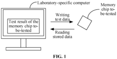
- FIG. 1 illustrates a schematic diagram of an application scenario of the method for testing the memory chip according to the disclosure.
- a server writes test data into memory cells of a memory chip to-be-tested, reads stored data from the memory cell after a period of time, and generates a test result of the memory chip to-be-tested according to the test data and the stored data.
- FIG. 2 illustrates a layout diagram of a memory chip to-be-tested according to an embodiment of the disclosure.
- multiple bit lines may be divided into 128 bit line groups, each bit line group has 8 bit lines, and the bit lines in each bit line group are designated as BL0, BL1, BL2... BL7 for a convenient description below.
- Multiple word lines may be divided into 8192 word line groups, each word line group has 8 word lines, and the bit lines in each bit line group are designated as WL0, WL1, WL2... WL7 for a convenient description below.
- Multiple memory cells P11 to P88 are distributed in a matrix, the memory cells in the first column are all connected to the word line WL0, the memory cells in the second column are all connected to the word line WL1, and so on, and the memory cells in the eighth column are all connected to the word line WL7; and the memory cells in the first row are all connected to the bit line BL0, the memory cells in the second row are all connected to the bit line BL1, and so on, and the memory cells in the eighth row are all connected to the bit line BL7, so that each memory cell is connected to a word line WL and a bit line BL.
- FIG. 3 illustrates a schematic structural diagram of a memory cell of a memory chip to-be-tested according to an embodiment of the disclosure.
- Each memory cell 10 includes a transistor 12 and the capacitor 11; a gate electrode of the transistor 12 is connected to a word line WL, a source electrode of the transistor 12 is connected to a bit line BL, and a drain electrode of the transistor 12 is connected to a capacitor 11. It should be noted that, the source electrode of the transistor 12 may further be connected to the capacitor 11, and accordingly, the drain electrode of the transistor 12 is connected to the bit line BL.
- a data line BL may write a high level signal "1" into a storage capacitor C, and when a signal on the word line WL switches off the switch transistor T, charges in the storage capacitor C leaks slowly with time.
- the time of leakage of the storage capacitor C from the high level signal "1" to the low level signal “0" is data storage time of the storage capacitor C.
- the data storage time of the storage capacitor C needs to be greater than a preset time to realize the dynamic storage function of the dynamic random access memory.
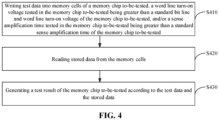
- FIG. 4 illustrates a schematic flowchart of a method for testing a memory chip according to an embodiment of the disclosure.
- the method for testing the memory chip includes the following operations.
- test data is written into memory cells of a memory chip to-be-tested; herein, a word line turn-on voltage tested in the memory chip to-be-tested is greater than a standard bit line and word line turn-on voltage of the memory chip to-be-tested, and/or a sense amplification time tested in the memory chip to-be-tested is greater than standard sense amplification time of the memory chip to-be-tested.
- a current leakage occurs between a gate electrode of a transistor 12 and a connected word line WL.
- the word line turn-on voltage tested in the memory chip to-be-tested is greater than the standard bit line and word line turn-on voltage of the memory chip to-be-tested, and/or the a sense amplification time tested in the memory chip to-be-tested is greater than the standard sense amplification time of the memory chip to-be-tested.
- the word line turn-on voltage refers to a turn-on voltage of the word line to which the memory cell is connected. If there exists a leakage current problem between the memory cell and the connected word line, increasing the turn-on voltage of the word line connected to the memory cell can enhance the leakage current effect between the memory cell and the connected word line, to able that the stored data changes more under the influence of leakage current, thereby being more conducive to judging whether the memory chip to-be-tested has a problem (leakage current problem) through operation S430.
- a standard bit line and word line turn-on voltage is 2.9V
- an increased word line turn-on voltage of a memory chip to-be-tested is between 2.95V to 3.2V.
- the sense amplification time refers to a sense time of a sense amplifier on a bit line. Adjusting the sense amplification time to be greater than standard sense delay time of the memory chip to-be-tested can further create a poor working condition for the memory chip to-be-tested, to able that the part in the memory chip to-be-tested and the part between the memory chip to-be-tested and a word line, which have problems, can be exposed more easily.
- a memory cell to-be-tested has problems, that is, a leakage current between the memory cell and the connected word line will not be generated, the leakage current effect between the memory cell and the connected word line will be enhanced after increasing the word line turn-on voltage tested in the memory chip to-be-tested and/or increasing the sense amplification time tested in the memory chip to-be-tested.
- a memory cell to-be-tested has no problems, a current between the memory cell and the connected word line will not be generated, the leakage current effect between the memory cell and the word line connected to the memory cell will not be enhanced after increasing the word line turn-on voltage tested in the memory chip to-be-tested and/or increasing the sense amplification time tested in the memory chip to-be-tested.
- Enhancing the leakage current effect between the memory cell and the word line connected to the memory cell can make it easier to judge whether the memory chip to-be-tested is damaged when performing operation S430.
- a tested word line turn-off voltage is applied to a word line connected to a memory cell, and the tested word line turn-off voltage of the memory chip to-be-tested is less than a standard bit line turn-off voltage of the memory chip to-be-tested.
- a substrate voltage of capacitance is applied to a capacitor terminal in the memory cell (the capacitor is arranged in the memory cell to store data), and the substrate voltage of capacitance tested in a memory chip to-be-tested is greater than a standard substrate voltage of capacitance of the memory chip to-be-tested.
- the substrate voltage of capacitance tested in the memory chip to-be-tested is greater than the standard substrate voltage of capacitance of the memory chip to-be-tested, to able that charges leaking from the memory cell and the connected word line are more easily attracted to the capacitor in the memory cell, thereby causing the written test data to change more obviously.
- the tested word line turn-off voltage applied to the word line (which is connected to the memory cell) is less than the standard bit line and word line turn-off voltage of the memory chip to-be-tested, and the substrate voltage of capacitance applied to the capacitor terminal is greater than the standard substrate voltage of capacitance of the memory chip to-be-tested.
- a standard bit line and word line turn-off voltage is -0.2V
- a tested word line turn-off voltage applied to a word line is -0.5V.
- a standard substrate voltage of capacitance is 0.5V
- the applied substrate voltage of capacitance is 0.8V
- only a word line turn-off voltage tested in a memory chip to-be-tested may be adjusted to be less than a standard bit line and word line turn-off voltage of the memory chip to-be-tested.
- only a word line turn-on voltage tested in a memory chip to-be-tested may be adjusted to be greater than a standard bit line and word line turn-on voltage of the memory chip to-be-tested.
- only sense amplification time tested in a memory chip to-be-tested may be adjusted to be greater than a standard sense amplification time of the memory chip to-be-tested.
- only a substrate voltage of capacitance tested in a memory chip to-be-tested may be adjusted to be greater than a standard substrate voltage of capacitance of the memory chip to-be-tested.
- a word line turn-off voltage tested in a memory chip to-be-tested may be adjusted to be less than a standard bit line and word line turn-off voltage of the memory chip to-be-tested, and a word line turn-on voltage tested in the memory chip to-be-tested may further be adjusted to be greater than a standard bit line and word line turn-on voltage of the memory chip to-be-tested.
- a word line turn-off voltage tested in a memory chip to-be-tested is adjusted to be less than a standard bit line and word line turn-off voltage of the memory chip to-be-tested; a word line turn-on voltage tested in the memory chip to-be-tested is adjusted to be greater than a standard bit line and word line turn-on voltage of the memory chip to-be-tested; and a sense amplification time tested in the memory chip to-be-tested is further adjusted to be greater than standard sense amplification time of the memory chip to-be-tested.
- a word line turn-off voltage tested in a memory chip to-be-tested is adjusted to be less than a standard bit line and word line turn-off voltage of the memory chip to-be-tested; a word line turn-on voltage tested in the memory chip to-be-tested is adjusted to be greater than a standard bit line and word line turn-on voltage of the memory chip to-be-tested; and a substrate voltage of capacitance tested in the memory chip to-be-tested is further adjusted to be greater than a standard substrate voltage of capacitance of the memory chip to-be-tested.
- the word line turn-on voltage, the word line turn-off voltage, the sense amplification time, and the substrate voltage of capacitance which are tested in the memory chip to-be-tested may be simultaneously adjusted. Specifically, the word line turn-off voltage tested in the memory chip to-be-tested is adjusted to be less than a standard bit line and word line turn-off voltage of the memory chip to-be-tested, the word line turn-on voltage tested in the memory chip to-be-tested is adjusted to be greater than a standard bit line and word line turn-on voltage of the memory chip to-be-tested, the sense amplification time tested in the memory chip to-be-tested is adjusted to be greater than the standard sense amplification time of the memory chip to-be-tested, and the substrate voltage of capacitance tested in the memory chip to-be-tested is adjusted to be greater than a standard substrate voltage of capacitance of the memory chip to-be-tested.
- the word line turn-off voltage tested in the memory chip to-be-tested may further be adjusted to be equal to the standard bit line and word line turn-off voltage of the memory chip to-be-tested.
- the word line turn-on voltage tested in the memory chip to-be-tested may be adjusted to be greater than the standard bit line and word line turn-on voltage of the memory chip to-be-tested.
- the sense amplification time tested in the memory chip to-be-tested may also be adjusted to be greater than standard sense amplification time of the memory chip to-be-tested.
- the substrate voltage of capacitance tested in the memory chip to-be-tested may also be adjusted to be greater than a standard substrate voltage of capacitance of the memory chip to-be-tested.
- the substrate voltage of capacitance tested in a memory chip to-be-tested may also be adjusted to be equal to a standard substrate voltage of capacitance of the memory chip to-be-tested.
- the word line turn-on voltage of the memory chip to-be-tested may be adjusted to be greater than the standard bit line and word line turn-on voltage of the memory chip to-be-tested.
- the sense amplification time of the memory chip to-be-tested may also be adjusted to be greater than the standard sense amplification time of the memory chip to-be-tested.
- the word line turn-off voltage of the memory chip to-be-tested may also be adjusted to be less than the standard bit line and word line turn-off voltage of the memory chip to-be-tested.
- a hold time may further be set after writing test data into memory cells of the memory chip to-be-tested and before reading stored data from the memory cell.
- the purpose of setting the hold time is such that if there exists leakage current, the leakage amount of leakage current increases over time, thereby influencing more on the test data written into the memory cells.
- the hold time is between 32ms and 192ms, and the hold time is set according to different test solutions.
- a substrate voltage of capacitance may be restored to a standard substrate voltage of capacitance and a word line turn-off voltage may be restored to a standard bit line and word line turn-off voltage after the hold time.
- a memory chip to-be-tested includes multiple columns of memory cells, and each column of memory cells adopts one or more detection cycles.
- test data When test data is written into memory cells of the memory chip to-be-tested, the test data may be written into the memory cells which are in the same detection cycle.
- stored data when stored data is read from memory cells, the stored data is also read from the memory cells which are in the same detection cycle.
- each column of memory cells of a memory chip to-be-tested may be tested in a traversal manner along the X-axis direction.
- the memory chip to-be-tested includes multiple rows of memory cells, and each row of memory cells adopts one or more detection cycles.
- test data When test data is written into the memory cells of the memory chip to-be-tested, the test data may be written into the memory cells which are in the same detection cycle. Similarly, when stored data is read from the memory cells, the stored data is also read from the memory cells which are in the same detection cycle.
- each column of memory cells of the memory chip to-be-tested may be tested in a traversal manner along the Y-axis direction.
- FIG. 2 illustrating a schematic layout diagram of the memory chip to-be-tested
- multiple memory cells P11 to P88 are distributed in a matrix
- the memory cells in the first column are all connected to the word line WL0
- the memory cells in the second column are all connected to the word line WL1, and so on
- the memory cells in the eighth column are all connected to the word line WL7
- the memory cells in the first row are all connected to the bit line BL0
- the memory cells in the second row are all connected to the bit line BL1, and so on
- the memory cells in the eighth row are all connected to the bit line BL7, so that each memory cell is connected to the word line WL and a bit line BL.
- the memory cell to-be-tested is a cell having functions of storing data and reading and writing data in the memory chip to-be-tested.
- Each memory cell includes a transistor (etched transistor) 12 and a capacitor 11.
- the etched transistor 12 is in a storage state (on or off) through charges of the capacitor 11.
- the capacitor which stores charges is represent by "1", and the capacitor which stores no charges is represent by "0".
- the test data may be used to test the memory cells in the memory chip to-be-tested. Due to the fact that the memory chip represents and stores a program and data in binary manner, the test data may be a binary sequence.
- the written test data may be binary sequence with equal data bits, and the test data has different data topologies.
- a data topology may include a data topology in which only "0" and “1” are adjacently arranged (e.g. 10101010, 01010101), and may further include a data topology in which 2N "0” and 2N “1” are adjacently arranged (e.g. 11001100, 00110011, 111110000, 00001111, and N is an integer greater than 1).
- the data topology is the data topology which only "0" and "1" are adjacently arranged, which can create a worse environment and make the leakage current effect between the memory cell and the connected word line more obvious.
- test data is written into the memory cells of the memory chip to-be-tested in a traversal access manner which is a column writing manner.
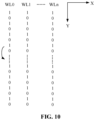
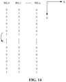
- writing test data will be illustrated below with reference to FIG. 7 to FIG. 14 .
- a data topology "0" (“10101010”
- a data topology "1” (“01010101”) is written into memory cells connected to word lines in order of columns.
- each memory cell when writing, it is written in a group of "10101010” or "01010101", and 8 data are written into each memory cell, i.e., each memory cell will write “10101010” or "01010101".
- each memory cell is cyclically written in order of word lines (WL0 to WLn) in the form of first column and then row. That is, memory cells P11, P21, P31... P81 connected to WL0 write the test data first, then the memory cells P12, P22, P32... P82 connected to WL1 write the test data, etc., and finally the memory cells P1n, P2n, P3n... P8n connected to WLn (e.g., n is 7) write the test data.
- test data When the test data is written into each column of memory cells of the memory chip to-be-tested, the test data is written into each memory cell in the same column in order of bit lines (BL0 to BLn). That is, when the test data is written into memory cells P11, P21, P31,...P81 connected to WL0, 8 data ("10101010” or "01010101") are sequentially written into each memory cell in order of P11 to P81. Similarly, when test data is written into memory cells P12, P22, P32... P82 connected to WL1, 8 data (“101010” or "01010101”) are written into each memory cell in order of P12 to P82. By analogy, when test data is written into memory cells P1n, P2n, P3n... P8n connected to WLn (e.g., n is 7), 8 data (“101010” or "01010101”) are written into each memory cell in order of P1n to P8n.
- bit lines BL0 to BLn
- stored data in the memory cells may be read in order of columns after standing for a period of time.
- the stored data refers to stored data obtained by reading the written test data from the memory cells of the memory chip, which may be used to check the read-write function of the memory cells.
- the operation of writing test data and reading stored data is performed cyclically on memory cells connected to each word line, so that the test for the memory chip to-be-tested can be completed.
- the leakage current effect of the memory chip to-be-tested can be enhanced before reading stored data by adjusting one or more of the word line turn-on voltage, the word line turn-off voltage, the sense amplification time and the substrate voltage of capacitance applied to a capacitor terminal which are tested in the memory chip to-be-tested.
- the sequence length of the test data is less than or equal to the number of memory cells in the memory chip to-be-tested. It also can be understood that, the number of bits of column memory cells in the memory chip to-be-tested is greater than the number of bits of written data.
- the number of bits of column memory cells is an integer multiple of the number of bits of written test data.
- the test data may be cyclically written, then the number of bits of row memory cells in the memory chip to-be-tested is greater than the number of bits of the written test data, and preferably, the number of bits of the row memory cells is an integer multiple of the number of bits of the written test data.
- the stored data is read from the memory cell.
- test data is written into memory cells of the memory chip to-be-tested in a traversal access manner which is a column writing manner; and accordingly, the data is read from the memory cells of the memory chip to-be-tested in a traversal access manner which is a column reading manner.
- each row of memory cells may adopt one or more detection cycles, i.e., each row of memory cells supports writing data and reading data for many times, and the more detection cycles, the higher accuracy of the test.
- a test result of the memory chip to-be-tested is generated according to the test data and the stored data.
- test data will change under the influence of leakage current after writing, thereby causing the stored data to be different from the test data.
- whether there exists leakage current between the memory cell and the connected word line in the memory chip to-be-tested can be judged, and if there exists the leakage current between the memory cell and the connected word line in the memory chip to-be-tested, it can be judged that the memory chip to-be-tested is a problematic chip.
- test data is compared with the stored data, whether the memory cells of the memory chip to-be-tested have a read-write error is determined according to a comparison result, and the test result of the memory chip to-be-tested is generated according to a determination result of whether the memory cells of the memory chip to-be-tested have the read-write error. If the read-write error occurs, the test result of the memory chip to-be-tested is determined to be that the memory chip to-be-tested is a problematic chip. If no read-write error occurs, or the read-write error occurs within a certain allowable range, the test result of the memory chip to-be-tested is determined to be that the memory chip to-be-tested is a chip without problems.
- test data may be cyclically written into each memory cell of the memory chip to-be-tested. If the memory cells of the memory chip to-be-tested have the read-write error, bits with the read-write error are determined according to the comparison result, the determination of occurring bits with the read-write error may be further used to judge which memory cells in the memory chip to-be-tested has a leakage current problem.
- the embodiments provide a method for testing a memory chip.
- a word line turn-on voltage tested in the memory chip to-be-tested is set to be greater than a standard bit line and word line turn-on voltage of the memory chip to-be-tested, and/or the sense amplification time tested in the memory chip to-be-tested is set to be greater than standard sense amplification time of the memory chip to-be-tested.
- the sense amplification time tested in the memory chip to-be-tested is set to be greater than standard sense amplification time of the memory chip to-be-tested.
- the method may further include that: a tested word line turn-off voltage applied to a word line is set to be less than a standard bit line and word line turn-off voltage, a substrate voltage of capacitance tested in the memory chip to-be-tested is set to be greater than a standard substrate voltage of capacitance, the written test data is set, etc., so that if there is a leakage current problem, more charges are leaked.
- the leakage current effect between a word line connected to the memory cells and the memory cells is enhanced, so that the test data written into the memory cells changes (the more leakage current, the more changes). Due to the fact that, leakage current may result in the change of stored data in the memory cells (the more leakage current, the more changes), the test result of the memory chip to-be-tested can be generated according to the test data and the stored data after reading the stored data from the memory cells.
- the leakage current effect is enhanced, the existence of the leakage current can be more effectively detected by comparing the written data with the read data, whether the memory chip to-be-tested exists a leakage current problem can be more effectively detected, and which the memory cells and the word lines having current leakage can be effectively detected.
- an embodiment of the disclosure further provides a device 20 for testing a memory chip, including a writing module 21, a reading module 22 and a processing module 23.
- the writing module 21 is configured to write test data into memory cells of a memory chip to-be-tested.
- the test data is written into the memory cells of the memory chip to-be-tested in a traversal access manner which is a column writing manner.
- the test data may be binary sequences having equal data bits, and the test data has different data topologies.
- the data topology may include a data topology in which only "0" and "1" are adjacently arranged, and further include a data topology in which 2N "0" and 2N "1" are adjacently arranged (N is an integer greater than 1).
- the number of bits of row memory cells or column memory cells in the memory chip to-be-tested is greater than the number of bits of the written test data.
- the number of bits of the row memory cells or the column memory cells is an integer multiple of the number of bits of the written test data.
- the reading module 22 is configured to read stored data from the memory cells.
- the test data is read from the memory cells of the memory chip to-be-tested in a traversal access manner which is a column reading manner.
- the operation from writing test data to reading stored data is defined as a detection cycle, and each row of memory cells adopts one or more detection cycles.
- the processing module 23 is configured to generate a test result of the memory chip to-be-tested according to the test data and the stored data.
- the processing module 23 is specifically configured to compare the test data with the stored data, and determine whether the memory cells of the memory chip to-be-tested have the read-write error according to a comparison result. If the memory cells of the memory chip to-be-tested have the read-write error, bits with the read-write error therein are determined according to the comparison result; and the test result of the memory chip to-be-tested is generated according to a determination result of whether the memory cells of the memory chip to-be-tested have the read-write error.
- the word line turn-on voltage tested in the memory chip to-be-tested is greater than a standard bit line and word line turn-on voltage of the memory chip to-be-tested, and/or the sense amplification time tested in the memory chip to-be-tested is greater than a standard sense amplification time of the memory chip to-be-tested.
- the word line turn-on voltage of the memory chip to-be-tested is between 2.95V and 3.2V.
- the device 20 further includes a voltage setting module 24.
- the voltage setting module 24 is configured to apply a tested word line turn-off voltage to a word line and apply a substrate voltage of capacitance to a tested capacitor terminal after writing the test data into memory cells of a memory chip to-be-tested.
- the word line turn-off voltage tested in the memory chip to-be-tested is less than a standard bit line and word line turn-off voltage of the memory chip to-be-tested; and the substrate voltage of capacitance tested in the memory chip to-be-tested is greater than a standard substrate voltage of capacitance of the memory chip to-be-tested.
- the voltage setting module 24 is configured to apply a tested word line turn-off voltage to a word line and apply a substrate voltage of capacitance to a capacitor terminal before reading stored data from the memory cells.
- the word line turn-off voltage tested in a memory chip to-be-tested is equal to a standard bit line and word line turn-off voltage of the memory chip to-be-tested; and the substrate voltage of capacitance tested in the memory chip to-be-tested is equal to a standard substrate voltage of capacitance of the memory chip to-be-tested.
- the word line turn-off voltage tested in the memory chip to-be-tested is -0.5V
- the substrate voltage of capacitance applied to the tested capacitor terminal is 0.8V
- the device 20 further includes a time setting module 25.
- the time setting module 25 is configured to set hold time after writing the test data into memory cells of the memory chip to-be-tested and before reading stored data from the memory cells.
- the implementation of the writing module 21, the reading module 22, the processing module 23, the voltage setting module 24, and the time setting module 25 can refer to relevant contents of the embodiments illustrated in FIG. 1 to FIG. 14 , which will not be repeated herein.
- the embodiments provide a device 20 for testing a memory chip.
- the device 20 is configured to set a word line turn-on voltage of the memory chip to-be-tested to be greater than a standard bit line and word line turn-on voltage of the memory chip to-be-tested, and/or set the sense amplification time of the memory chip to-be-tested to be greater than the standard sense amplification time of the memory chip to-be-tested before writing test data into memory cells of the memory chip to-be-tested.
- a worse environment is created for the memory cells of the memory chip to-be-tested, and the leakage current effect can be exposed more easily.
- the device may be further configured to set a tested word line turn-off voltage applied to a word line to be less than a standard bit line and word line turn-off voltage, set a substrate voltage of capacitance of a memory chip to-be-tested to be greater than a standard substrate voltage of capacitance, and set written test data, etc., so that if there is a leakage current problem, more charges are leaked.
- the leakage current effect between the word line connected to the memory cells and the memory cells is enhanced, so that the test data written into the memory cells changes (the more leakage current, the more changes). Due to the fact that leakage current may result in the change of stored data in the memory cells (the more leakage current, the more changes), the test result of the memory chip to-be-tested can be generated according to the test data and the stored data after reading the stored data from the memory cells.
- the leakage current effect is enhanced, the existence of the leakage current can be more effectively detected by comparing the written data with the read data, whether memory chip to-be-tested exists a leakage current problem can be more effectively detected, and which memory cells and word lines having current leakage therebetween can be effectively detected.
- the disclosure further provides an electronic device 30, including at least one processor 31 and a memory 32 storing computer-executable instructions.
- the at least one processor 31 is configured to execute the computer-executable instructions stored in the memory 32 to implement the method for testing the memory chip according to any one of the foregoing embodiments.
- a memory 32 may be either independent from or integrated with the processor 31.
- the electronic device 30 may further include a bus 33 configured to connect the memory 32 and the processor 31 when the memory 32 is independently arranged.
- the disclosure further provides a computer-readable storage medium having stored therein computer-executable instructions that when executed by a processor, implement a method for testing a memory chip according to any one of the foregoing embodiments.
- the disclosure further provides a computer program product including a computer program configured to implement a method for testing a memory chip according to any one of the foregoing embodiments.
- the processor may be a Central Processing Unit ( CPU), another general-purpose processor, a Digital Signal Processor (DSP), an Application Specific Integrated Circuit (ASIC), etc.
- the general-purpose processor may be a microprocessor, or any common processor, etc. Steps of themethod for testing a memory chip according to the disclosure may be implemented directly by a hardware processor or by combined hardware and software modules in the processor.
- the memory may include a high-speed Random Access Memory (RAM), may further include an Non-Volatile Memory (NVM), e.g., at least a magnetic disk, and may further include a USB flash disk, a removable hard disk, a Read-Only Memory (ROM), a magnetic disk or an optical disk, etc.
- RAM Random Access Memory
- NVM Non-Volatile Memory
- ROM Read-Only Memory
- the bus may be an Industry Standard Architecture (ISA) bus, a Peripheral Component Interconnect (PCI) bus, an Extended Industry Standard Architecture (EISA) bus, etc. Buses may be divided into an address bus, a data bus, a control bus, etc. For convenient illustration, the bus as illustrated in the drawings of the disclosure is not limited to merely one bus or one type of bus.
- ISA Industry Standard Architecture
- PCI Peripheral Component Interconnect
- EISA Extended Industry Standard Architecture
- the foregoing computer-readable storage medium may be a ROM, a Programmable ROM (PROM), an Erasable Programmable ROM (EPROM), an Electrically Erasable Programmable ROM (EEPROM), a Ferromagnetic Random Access Memory (FRAM), a flash memory, a magnetic platter memory, and an optical disk or Compact Disc ROM (CD-ROM).
- PROM Programmable ROM
- EPROM Erasable Programmable ROM
- EEPROM Electrically Erasable Programmable ROM
- FRAM Ferromagnetic Random Access Memory
- flash memory a magnetic platter memory
- CD-ROM Compact Disc ROM
- all or partial steps of the foregoing method embodiments may be implemented by program instructions related to hardware.
- the foregoing program may be stored in a computer-readable storage medium.
- the program is executed to implement steps of the foregoing method embodiments; and the foregoing medium may be one capable of storing program codes, e.g., ROM, RAM, magnetic disk, or an optical disk.
- the disclosed device and method may be implemented in other ways.
- the device embodiments described above are merely illustrative, e.g., the modules are merely divided according to logical functions thereof, which may be divided in other ways in actual implementation, e.g., multiple modules may be combined or integrated into another system, or some features may be omitted or not implemented.
- each functional module may be integrated into a processing unit, or each module may be arranged physically alone, or two or more modules may be integrated into one unit.
- the integrated unit of the foregoing modules may be implemented either in the form of hardware or in the form of a functional unit of hardware and software.
- the integrated modules implemented as a functional module of software may be stored in a computer-readable storage medium.
- the functional module of software may be stored in a storage medium and include instructions enabling a computer device (which may be a personal computer, a server, a network device, etc.) or a processor to implement partial steps of the method according to the embodiments of the disclosure.
- the method according to the foregoing embodiments may be implemented by means of software with a necessary common hardware platform, and further may be implemented by means of hardware. In many cases, however, the former is preferred. Thereon, the technical solution of the disclosure in essence or the part thereof contributing to the prior art may be embodied as a software product.
- the computer software product is stored in a storage medium (e.g. ROM/RAM, magnetic disk, and optic disk) and includes instructions enabling a terminal device (which may be a mobile phone, a computer, a server, an air conditioner, or a network device, etc.) to implement the method according to the embodiments of the disclosure.
- each process and/or block in a flowchart and/or block diagram, and a combination thereof may be implemented by computer program instructions.
- the computer program instructions may be stored in a processor of a general-purpose computer, a special-purpose computer, an embedded processor, or another programmable data processing device to form a machine device, so that the instructions executed by the processor of the computer or another programmable data processing device form a device configured to implement a function specified in one or more steps of a flowchart and/or one or more blocks of a block diagram.
- the computer program instructions may further be stored in a computer-readable memory capable of directing a computer or another programmable data processing device to operate in a specific manner, and the instructions stored in the computer-readable memory form a manufactured product including an instruction device to implement the function specified in one or more steps of a flowchart and/or one or more blocks of a block diagram.
- the computer program instructions may further be loaded into a computer or another programmable data processing device, therefore a set of steps are implemented in the computer or another programmable data processing device to form a computer-implemented process, and the instructions executed by the computer or another programmable data processing device provide the steps implementing the function specified in one or more steps of a flowchart and/or one or more blocks of a block diagram.
Landscapes
- For Increasing The Reliability Of Semiconductor Memories (AREA)
Applications Claiming Priority (2)
| Application Number | Priority Date | Filing Date | Title |
|---|---|---|---|
| CN202210153533.8A CN116665749A (zh) | 2022-02-18 | 2022-02-18 | 存储芯片的测试方法及其装置 |
| PCT/CN2022/086403 WO2023155284A1 (fr) | 2022-02-18 | 2022-04-12 | Procédé de test pour puce de mémoire et dispositif associé |
Publications (2)
| Publication Number | Publication Date |
|---|---|
| EP4258266A1 true EP4258266A1 (fr) | 2023-10-11 |
| EP4258266A4 EP4258266A4 (fr) | 2024-04-17 |
Family
ID=87574798
Family Applications (1)
| Application Number | Title | Priority Date | Filing Date |
|---|---|---|---|
| EP22731977.9A Pending EP4258266A4 (fr) | 2022-02-18 | 2022-04-12 | Procédé de test pour puce de mémoire et dispositif associé |
Country Status (2)
| Country | Link |
|---|---|
| US (1) | US11901024B2 (fr) |
| EP (1) | EP4258266A4 (fr) |
Families Citing this family (1)
| Publication number | Priority date | Publication date | Assignee | Title |
|---|---|---|---|---|
| CN117935893B (zh) * | 2024-03-21 | 2024-07-16 | 成都佰维存储科技有限公司 | 一种eMMC四角测试方法、装置、可读存储介质及电子设备 |
Family Cites Families (16)
| Publication number | Priority date | Publication date | Assignee | Title |
|---|---|---|---|---|
| JPH0620465A (ja) * | 1991-09-02 | 1994-01-28 | Mitsubishi Electric Corp | 半導体記憶装置 |
| JPH06176585A (ja) * | 1992-12-07 | 1994-06-24 | Fujitsu Ltd | 半導体記憶装置 |
| US6105152A (en) | 1993-04-13 | 2000-08-15 | Micron Technology, Inc. | Devices and methods for testing cell margin of memory devices |
| CN1187677A (zh) | 1997-01-09 | 1998-07-15 | 三菱电机株式会社 | 动态型半导体存储器及其测试方法 |
| US6016281A (en) | 1997-12-17 | 2000-01-18 | Siemens Aktiengesellschaft | Memory with word line voltage control |
| JP2011502326A (ja) * | 2007-10-29 | 2011-01-20 | アギア システムズ インコーポレーテッド | メモリ・デバイスをテストする方法および機器 |
| US8159881B2 (en) | 2009-06-03 | 2012-04-17 | Marvell World Trade Ltd. | Reference voltage optimization for flash memory |
| KR101735091B1 (ko) | 2010-08-30 | 2017-05-16 | 에스케이하이닉스 주식회사 | 컬럼소스신호 생성회로 |
| US8780654B2 (en) * | 2012-04-10 | 2014-07-15 | Apple Inc. | Weak bit detection in a memory through variable development time |
| US9810723B2 (en) * | 2012-09-27 | 2017-11-07 | Sandisk Technologies Llc | Charge pump based over-sampling ADC for current detection |
| CN104810062A (zh) | 2015-05-12 | 2015-07-29 | 东南大学 | 一种sram芯片的puf特性测试方法及装置 |
| KR20170015795A (ko) * | 2015-07-31 | 2017-02-09 | 에스케이하이닉스 주식회사 | 반도체 메모리 장치 및 테스트 방법 |
| KR102772756B1 (ko) * | 2016-10-17 | 2025-02-26 | 에스케이하이닉스 주식회사 | 메모리 장치 및 메모리 장치의 동작 방법 |
| KR102132196B1 (ko) | 2018-09-05 | 2020-07-09 | 고려대학교 산학협력단 | 피드백 루프 동작을 이용하는 피드백 전계효과 전자소자 및 이를 이용한 배열 회로 |
| JP2020113351A (ja) * | 2019-01-10 | 2020-07-27 | キオクシア株式会社 | メモリチップ |
| CN113012745B (zh) | 2021-03-23 | 2022-05-31 | 长鑫存储技术有限公司 | 存储器的检测方法及检测装置 |
-
2022
- 2022-04-12 EP EP22731977.9A patent/EP4258266A4/fr active Pending
- 2022-06-28 US US17/851,656 patent/US11901024B2/en active Active
Also Published As
| Publication number | Publication date |
|---|---|
| EP4258266A4 (fr) | 2024-04-17 |
| US20230268019A1 (en) | 2023-08-24 |
| US11901024B2 (en) | 2024-02-13 |
Similar Documents
| Publication | Publication Date | Title |
|---|---|---|
| CN116665749A (zh) | 存储芯片的测试方法及其装置 | |
| CN113012745A (zh) | 存储器的检测方法及检测装置 | |
| CN114187955B (zh) | 存储器阵列的测试方法、装置、设备及存储介质 | |
| CN110164496B (zh) | 半导体存储器元件及其读取方法 | |
| CN113257332A (zh) | 一种闪存的有效性预测方法、装置及存储介质 | |
| CN114743583A (zh) | 存储器失效测试方法及装置、存储介质及电子设备 | |
| US11901024B2 (en) | Method and device for testing memory chip | |
| CN114333961B (zh) | 存储器阵列的测试方法、装置、设备及存储介质 | |
| CN111949426A (zh) | 一种固件程序错误的检测方法、装置及存储设备 | |
| US6587378B2 (en) | Apparatus and method for refreshing a flash memory unit | |
| US20080082776A1 (en) | Memories, method of storing data in a memory and method of determining memory cell sector quality | |
| US20230230649A1 (en) | Method and device for testing memory chip | |
| CN116798500A (zh) | 存储芯片的测试方法及设备 | |
| CN116504296A (zh) | 存储芯片的测试方法及设备 | |
| CN117012265A (zh) | 存储器测试方法、装置、电子设备及存储介质 | |
| US20230063964A1 (en) | Electronic device, over-erase detection and elimination methods for memory cells | |
| CN111951869B (zh) | 一种非易失存储器读处理方法及装置 | |
| CN108614666A (zh) | 基于NANDflash的数据块处理方法和装置 | |
| CN115620767B (zh) | 存储器的检测方法和存储器的检测装置 | |
| CN111951860A (zh) | 一种非易失存储器写处理方法及装置 | |
| CN111951854A (zh) | 一种非易失存储器写处理方法及装置 | |
| CN116486880B (zh) | 存储器的检测方法 | |
| US12524164B2 (en) | Memory device, memory system and operation method thereof, and electronic apparatus | |
| CN119889407B (zh) | 存储阵列的修复方法及存储器 | |
| KR20240124081A (ko) | 패스 전압을 조절하는 메모리 장치 및 그 동작 방법 |
Legal Events
| Date | Code | Title | Description |
|---|---|---|---|
| STAA | Information on the status of an ep patent application or granted ep patent |
Free format text: STATUS: UNKNOWN |
|
| STAA | Information on the status of an ep patent application or granted ep patent |
Free format text: STATUS: THE INTERNATIONAL PUBLICATION HAS BEEN MADE |
|
| PUAI | Public reference made under article 153(3) epc to a published international application that has entered the european phase |
Free format text: ORIGINAL CODE: 0009012 |
|
| STAA | Information on the status of an ep patent application or granted ep patent |
Free format text: STATUS: REQUEST FOR EXAMINATION WAS MADE |
|
| 17P | Request for examination filed |
Effective date: 20220629 |
|
| AK | Designated contracting states |
Kind code of ref document: A1 Designated state(s): AL AT BE BG CH CY CZ DE DK EE ES FI FR GB GR HR HU IE IS IT LI LT LU LV MC MK MT NL NO PL PT RO RS SE SI SK SM TR |
|
| REG | Reference to a national code |
Ref country code: DE Ref legal event code: R079 Free format text: PREVIOUS MAIN CLASS: G11C0029120000 Ipc: G11C0029500000 |
|
| RIC1 | Information provided on ipc code assigned before grant |
Ipc: G11C 29/00 20060101ALI20231218BHEP Ipc: G11C 29/12 20060101ALI20231218BHEP Ipc: G11C 29/50 20060101AFI20231218BHEP |
|
| A4 | Supplementary search report drawn up and despatched |
Effective date: 20240314 |
|
| RIC1 | Information provided on ipc code assigned before grant |
Ipc: G11C 29/00 20060101ALI20240308BHEP Ipc: G11C 29/12 20060101ALI20240308BHEP Ipc: G11C 29/50 20060101AFI20240308BHEP |
|
| DAV | Request for validation of the european patent (deleted) | ||
| DAX | Request for extension of the european patent (deleted) | ||
| STAA | Information on the status of an ep patent application or granted ep patent |
Free format text: STATUS: EXAMINATION IS IN PROGRESS |
|
| 17Q | First examination report despatched |
Effective date: 20260225 |