EP4258298A1 - Procédé de fabrication de bobines supraconductrices et dispositif - Google Patents
Procédé de fabrication de bobines supraconductrices et dispositif Download PDFInfo
- Publication number
- EP4258298A1 EP4258298A1 EP22305437.0A EP22305437A EP4258298A1 EP 4258298 A1 EP4258298 A1 EP 4258298A1 EP 22305437 A EP22305437 A EP 22305437A EP 4258298 A1 EP4258298 A1 EP 4258298A1
- Authority
- EP
- European Patent Office
- Prior art keywords
- layer
- stacking
- chamber
- vapor deposition
- temperature
- Prior art date
- Legal status (The legal status is an assumption and is not a legal conclusion. Google has not performed a legal analysis and makes no representation as to the accuracy of the status listed.)
- Withdrawn
Links
Images


Classifications
-
- H—ELECTRICITY
- H01—ELECTRIC ELEMENTS
- H01F—MAGNETS; INDUCTANCES; TRANSFORMERS; SELECTION OF MATERIALS FOR THEIR MAGNETIC PROPERTIES
- H01F41/00—Apparatus or processes specially adapted for manufacturing or assembling magnets, inductances or transformers; Apparatus or processes specially adapted for manufacturing materials characterised by their magnetic properties
- H01F41/02—Apparatus or processes specially adapted for manufacturing or assembling magnets, inductances or transformers; Apparatus or processes specially adapted for manufacturing materials characterised by their magnetic properties for manufacturing cores, coils, or magnets
- H01F41/04—Apparatus or processes specially adapted for manufacturing or assembling magnets, inductances or transformers; Apparatus or processes specially adapted for manufacturing materials characterised by their magnetic properties for manufacturing cores, coils, or magnets for manufacturing coils
- H01F41/048—Superconductive coils
-
- H—ELECTRICITY
- H01—ELECTRIC ELEMENTS
- H01F—MAGNETS; INDUCTANCES; TRANSFORMERS; SELECTION OF MATERIALS FOR THEIR MAGNETIC PROPERTIES
- H01F6/00—Superconducting magnets; Superconducting coils
- H01F6/06—Coils, e.g. winding, insulating, terminating or casing arrangements therefor
-
- H—ELECTRICITY
- H10—SEMICONDUCTOR DEVICES; ELECTRIC SOLID-STATE DEVICES NOT OTHERWISE PROVIDED FOR
- H10N—ELECTRIC SOLID-STATE DEVICES NOT OTHERWISE PROVIDED FOR
- H10N60/00—Superconducting devices
- H10N60/01—Manufacture or treatment
- H10N60/0268—Manufacture or treatment of devices comprising copper oxide
- H10N60/0296—Processes for depositing or forming copper oxide superconductor layers
- H10N60/0436—Processes for depositing or forming copper oxide superconductor layers by chemical vapour deposition [CVD]
- H10N60/0464—Processes for depositing or forming copper oxide superconductor layers by chemical vapour deposition [CVD] by metalloorganic chemical vapour deposition [MOCVD]
-
- H—ELECTRICITY
- H10—SEMICONDUCTOR DEVICES; ELECTRIC SOLID-STATE DEVICES NOT OTHERWISE PROVIDED FOR
- H10N—ELECTRIC SOLID-STATE DEVICES NOT OTHERWISE PROVIDED FOR
- H10N60/00—Superconducting devices
- H10N60/01—Manufacture or treatment
- H10N60/0268—Manufacture or treatment of devices comprising copper oxide
- H10N60/0801—Manufacture or treatment of filaments or composite wires
Definitions
- the present disclosure is related to methods or processes and devices for manufacturing superconducting coils. More specifically it is related to methods or devices that involve a multistage coating of a surface of a structure.
- the structure may be for example a cylinder in its broader definition, that is, a surface in space made of parallel straight lines (generating lines), and the surface may be an inner or an outer surface of the cylinder.
- HTS High-Temperature Superconductors
- magnets are constructed with large magnets that are shaped into the form of a coil; magnets may be either permanent or electrical depending on cost or application.
- the coil In applications where the field needs a special configuration, for instance, in stellarators, the coil must be twisted to a complicated shape during construction. This greatly increases costs during the design phase; stellarator design is very complicated and requires a lot of testing, so constructing many magnets coils requires a lot of time and of money.
- a method for constructing superconducting coils is described in U.S. Pat. No. 8,655,423 to Miyazaki, et al.
- Miyazaki describes a superconducting coil formed of several layers of different materials. A group of these layers is described as constituting a superconducting coil portion which is formed of thin-film superconducting wires.
- the coils described by Miyazaki and those that are common in the art are constructed by arranging superconducting films, also called superconducting tapes, into the shape of wires and the wires are then further configured into the shape of coils.
- superconducting coils are formed by stacking superconducting films or layers so that electric current may flow in a desired direction and produce the appropriate magnetic field configuration.
- the tapes themselves can be constructed through several methods described in the art.
- US Pat. No. 10, 935, 799 to Majkic, et al. a method for fabricating high quality superconducting tapes is disclosed.
- the method of Majkic is limited to applications that require a very thin tape structure. It is not apparent from the description of Majkic how the process may defeat the limitations of, for example, different tape geometries.
- the method described in this prior art is limited to the rectangular shape of the appropriate size.
- One embodiment addresses all or some of the drawbacks of known methods and devices for constructing superconducting coils.
- One embodiment provides a method for manufacturing a superconducting coil, the method comprising steps of:
- the method further comprises, after the rotating step and before forming the first stacking, a step of electropolishing the structure in a wet chamber, for example using an electrolytic solution and electrodes.
- the wet chamber, the cold chamber and the hot chamber are a single chamber.
- the wet chamber, the cold chamber and the hot chamber are separate chambers.
- the temperature in the cold chamber (103) is the room temperature.
- the temperature in the hot chamber is higher than 500°C.
- forming the first stacking comprises at least a physical vapor deposition step, like sputtering, for example magnetron sputtering, inclined substrate deposition, ion beam deposition and/or ion beam assisted deposition.
- a physical vapor deposition step like sputtering, for example magnetron sputtering, inclined substrate deposition, ion beam deposition and/or ion beam assisted deposition.
- forming the first stacking comprises:
- forming the second stacking comprises at least a physical vapor deposition step, for example sputtering or pulsed laser deposition, and/or a chemical vapor deposition step, for example a metal organic chemical vapor deposition step.
- forming the second stacking comprises depositing at least a layer of a superconductive material, for example rare-earth barium copper oxide or yttrium barium copper oxide, using metal-organic chemical vapor deposition, for example using a vaporized precursor at a uniform temperature and laminar flow, or using pulsed laser deposition.
- a superconductive material for example rare-earth barium copper oxide or yttrium barium copper oxide
- metal-organic chemical vapor deposition for example using a vaporized precursor at a uniform temperature and laminar flow, or using pulsed laser deposition.
- forming the second stacking comprises a step of depositing a layer of a low-resistivity material like silver on the superconductive material layer.
- forming the second stacking comprises:
- the cooling step comprises injecting an inert gas or vapor at a fourth temperature lower than the third temperature.
- the step of depositing the sixth layer comprises filling in the hot chamber a vaporized superconductive material precursor at a fifth temperature, for example between 250°C and 280°C.
- the method further comprises heating the structure to a second temperature higher than the first temperature, for example between 800°C and 900°C, between depositing the fifth layer and depositing the sixth layer.
- the method further comprises repeating the steps of forming the second stacking, in the same or in different order, in order to form at least multiple second stackings on the first stacking, preferably several times, for example between 4 and 80 times.
- the method further comprises, preferably after the step of forming the second stacking or the multiple second stackings:
- One embodiment provides a superconducting coil obtained by the method according to an embodiment, the superconducting coil comprising:
- the stacking comprises multiple second stackings, with the layers of the different second stackings being in the same or in a different order.
- the structure is composed of Hastelloy or covered by an Hastelloy layer.
- the structure is a cylinder.
- One embodiment provides a device for manufacturing a superconducting coil comprising a structure, wherein the device is adapted to implement the method according to an embodiment, and comprises:
- the structure is a right circular cylinder (cylinder 202 ) and the surface to be coated is an outer surface of said cylinder.
- the surface to be coated may be an inner surface of the cylinder.
- Other shapes of a structure having a surface to be coated are possible.
- the surface to be coated could be an inner or an outer surface of a non-circular and/or non-right cylinder, or any other appropriate structure.
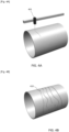
- FIG. 2 is a perspective view of an embodiment of a device 200 for manufacturing superconducting coils using multistage coating.
- the device comprises rotating rods 204 adapted to held a flat-faced ring or hollow cylinder 202, which is not necessarily included in the device.
- the cylinder 202 may be constructed of a material like Hastelloy.
- the rods 204 adapted to hold the cylinder 202 may also be batons, large discs, cylinders, or wheels.
- the rods 204 should be able to rotate, this can be done through the use of a motor or other appropriate means. Further, the cylinder 202 should be held on the rods 204 by means that would allow for the cylinder 202 to rotate with the rods 204.
- At least one of the rods 204 may be connected to a heating ring or resistor 206.
- the heating resistor 206 heat the rod 204 which in turn heat the cylinder 202.
- the rods 204 could act as electrodes used to pass current through the cylinder 202 in order to heat it.
- the device from FIG. 2 may be housed inside a chamber, which is appropriate for performing operations like chemical vapor deposition CVD, metal-organic chemical vapor deposition MOCVD, or magnetron sputtering, among others.
- Other heating methods may be used instead of the heating resistor 206, other embodiments may use at least an inductive or ohmic heating coil which could be included in the inside of the cylinder 202.
- this includes a flat-faced ring or a hollow cylinder.
- FIG. 1 is a diagram of an embodiment of a method for manufacturing superconducting coils. The method is divided into three mayor phases or stages, indicated as such because the processes in the stage occur in three different chambers: a wet chamber 101, a cold chamber 103, and a hot chamber 105.
- the wet chamber 101 may be filled by an electrolytic solution to perform electropolishing 106 on the surface of the cylinder 202. Therefore, the wet chamber 101 may also include electrodes for this end.
- a physical vapor deposition (PVD) technique In the cold chamber 103, several processes may occur, based on a physical vapor deposition (PVD) technique.
- PVD physical vapor deposition
- IBAD ion beam assisted deposition
- PVD techniques may be used in the cold chamber, which may depend on the material to deposit. For example:
- the cold chamber 103 preferably includes at least an ejector, like a target or a nozzle, and/or may include a source, depending on the technique used, for example for magnetron sputtering and IBAD.
- this may include a target or a nozzle, depending on the technique used.
- the hot chamber 105 involves several processes based on a physical vapor deposition (PVD) technique and/or a chemical vapor deposition (CVD) technique.
- PVD physical vapor deposition
- CVD chemical vapor deposition
- at least six processes may be involved, including: the heating of the cylinder 202 to a temperature between 700°C and 800°C (first temperature) in the heating to between 700°C and 800°C step 120 ; three CVD and/or PVD steps adapted to deposit materials, the MgO step 118 adapted to deposit (MgO), the LMO step 116 adapted to deposit lanthanum manganite (LMO), and the REBCO step 114 adapted to deposit rare-earth barium copper oxide (REBCO), or another appropriate superconducting material; the cooling of the cylinder 202 to between 450°C and 600°C (third temperature), for example between 500°C and 600°C, in the cooling between 450°C and 600°C step 124 ; and a CVD or a PV
- the cylinder may be heated again in the heating to between 700°C and 800°C step 120, for example to repeat, at least once, the process steps in the hot chamber, or the cylinder 202 may be stopped in the stop rotation of cylinder step 126.
- the method may also comprise a cool to room temperature step 128, before, after or during the stop rotation of cylinder step 126, where the process ends.
- the cooling to between 450°C and 600°C step 124 may be envisioned to be done through convective heating, by injecting a gas or vapor that is inert at a lower temperature (fourth temperature), but other ways may also be possible.
- CVD or PVD techniques may be used in the hot chamber, which may depend on the material to deposit. For example:
- a heating to between 800°C and 900°C step 115 may be needed between the LMO step 116 and the REBCO step 114, in order to heat the cylinder 202 to a temperature adapted to the REBCO step 114.
- the hot chamber 105 preferably includes at least an ejector like a nozzle for the execution of the CVD and/or PVD processes, depending on the technique(s) used.
- the temperature ranges in the cold and hot chambers are given in relation with the techniques used and the materials to deposit. The person skilled in the art will know how to adapt them for other techniques and/or other materials.
- the processes in the three chambers, wet 101, cold 103 and hot 105 chambers, may be executed in three separate chambers, meaning that the cylinder would have to be taken out of one chamber and placed in the next one, or they could all be executed in a single chamber.
- the illustrated method starts in the wet chamber 101.
- a cylinder 202 like the one from FIG. 2 is made to rotate in the start rotation of cylinder step 104.
- the rods 204 rotate the cylinder 202.
- the cylinder 202 is submerged in an electrolytic solution and, alongside appropriate electrodes, an electropolishing process polishes the surface in the electropolishing step 106.
- the electropolishing process may be accompanied by rinsing steps before and after the polishing and by drying afterwards. Further, the electropolishing step 106 may be repeated several times to achieve a certain level of polish. In an embodiment where the wet chamber 101 and the cold chamber 103 are separated, the cylinder 202 would now be taken into the cold chamber 103.
- a magnetron sputtering ejector like a target or a nozzle, deposits layers of alumina and yttria, and a target of IBAD deposits magnesium oxide MgO.
- the first step in the cold chamber 103 is the sputtering of alumina step 108.
- a magnetron sputtering ejector injects aluminum and oxygen into the chamber, depositing alumina on the surface of the cylinder 202.
- the same or another magnetron sputtering ejector injects yttrium and oxygen into the chamber, depositing yttria on the cylinder surface, in the second step called sputtering of yttria step 110.
- the last step in the cold chamber is the deposition of MgO through the use of ion beam assisted deposition using a target of magnesium and oxygen. This step is called the IBAD MgO step 112.
- the steps in the cold chamber 103 can be executed at room temperature. Nevertheless, for the next steps in the method, the surface of the cylinder 202 must be heated. The cylinder 202 must then be transferred to a different chamber that may heat its surface or it may also be possible to heat it using the heating resistors 206.
- the first step in the hot chamber 105 is the heating of the cylinder between 700°C and 800°C in the heating to between 700°C and 800°C step 120.
- MOCVD metalorganic chemical vapor deposition MOCVD can be used to deposit MgO and LMO on top of the materials deposited on the cold chamber 103.
- MOCVD is used to deposit MgO in the MgO step 118.
- the hot chamber 105 is filled with a vaporized MgO precursor at an uniform temperature and exhibiting laminar flow around the cylinder 202, thus depositing MgO on its surface.
- the same process is repeated in the LMO step 116, this time using a lanthanum manganite LMO precursor at an uniform temperature and laminar flow.
- the temperature in the hot chamber 105 may be increased further to 850°C, for example between 850°C and 890°C, in the heating to between 800°C and 900°C step 115 before the REBCO step 114.
- a superconducting material like rare-earth barium copper oxide may be filled with a vaporized REBCO precursor exhibiting laminar flow around the cylinder 202.
- the temperature of the REBCO precursor would be between 250°C and 280°C (fifth temperature).
- pulsed laser deposition PLD
- MOCVD pulsed laser deposition
- the cylinder 202 is cooled in the next step in the cooling to between 450°C and 600°C step 124. At this temperature it is possible to use chemical-vapor deposition or metal-organic chemical vapor deposition to deposit silver on the surface of the cylinder. Silver is deposited in the Ag step 122.
- the cylinder 202 may be made to stop by stopping the rods 204, this is the stop rotation of cylinder step 126. Once the cylinder 202 has been stopped, it may be left to cool to room temperature, in the cool to room temperature step 128. Afterwards, the cylinder 202 may be removed from the chamber and it may then be cut or used as per the needs of the application.
- FIG. 3 An example of superconducting coil 300 constructed by following the diagram from FIG. 1 would be composed of chemically or otherwise bonded layers as shown in FIG. 3 .
- the very first layer is the Hastelloy layer 302, which may be polished in the electropolishing step 106 in the wet chamber 101. Once the cylinder 202 is in the cold chamber 103, the other layers are added.
- a layer of alumina is sputtered in the sputtering of alumina step 108, this is the alumina layer 304.
- yttria is sputtered as part of the sputtering of yttria step 110, this is the yttria layer 306.
- a layer of MgO is deposited, this is done in the IBAD MgO step 112 and results in the first MgO layer 308.
- the cylinder 202 is then introduced into the hot chamber 105 and the last layers are added.
- the next layer to be added is a second MgO layer 310.
- a second MgO layer 310 is deposited through the use of MOCVD on top of the first MgO layer 308.
- the MOCVD process is also used to deposit a layer of lanthanum manganite LMO on top of the second MgO layer 310, this is the LMO layer 312.
- MOCVD is used once again to deposit a layer of REBCO on top of the LMO layer 312, this is the REBCO layer 314.
- CVD or MOCVD is preferably used to deposit a layer of silver Ag on top of the REBCO layer 314, this is the silver layer 316.
- Forming the silver layer using (MO)CVD has an advantage, compared to a sputtering technique for example, of forming a layer with a suitable crystal, which can be beneficial if a new sequence of layers is formed on the silver layer.
- All the layers formed in the cold chamber may be called “first stacking of layers” or “first stacking”, and all the layers formed in the hot chamber may be called “second stacking of layers” or “second stacking”.
- the alumina, yttria, MgO, LMO layers may be called "buffer layers".
- the buffer layers may form an appropriate template for the formation of the superconducting layer.
- the final four layers, second MgO layer 310, LMO layer 312, REBCO layer 314 and silver layer 316 may be deposited repeatedly in the same or different order. They may be deposited repeatedly on top of the layers deposited during the process in the cold chamber 103 in order to create a layer stack or wafer of between 4 and 80, for example between 20 and 40 layers.
- an yttrium stabilized zirconia (YSZ) layer may be formed, using a PVD technique like sputtering, ISD, IBD or IBAD, and instead of the MgO layer in the hot chamber, an epitaxial YSZ layer may be formed, using for example CVD, MOCVD, or a PVD technique like IBAD.
- YSZ yttrium stabilized zirconia
- the following sequence may be formed on the Hastelloy layer 302 preferably in the following order:
- REBCO rare-earth materials that exhibit high-temperature superconductivity, like YBCO.
- the last silver layer that is, the silver layer of the last sequence of layers in case of repetition of layers 310, 312, 314, 316, may be replaced by a copper layer.
- the silver layer is particularly adapted as a starting layer for a repetition of layers, but is of less interest in the last sequence on which no repetition is made, and a copper layer is cheaper, faster to grow using electroplating for example and harder than silver.
- an additional step of removing material at least from the silver layer, the superconductive layer and possibly the buffering layers may be provided, in order to create a pattern that form grooves 410, as illustrated in figure 4B .
- the pattern shape may depend on the application.
- a technique like laser patterning 401 may be used, as illustrated in figure 4A .
- Other techniques, like a mechanical technique or photolithography may be used.
- the grooves may be filled with a metal, for example silver.
- the cylinder of the superconducting coil may be machined to have a particular shape, and the superconducting coil may be assembled to another superconducting coil, of a similar or different shape, like several modular coils, to form an assembly. For example, several superconducting coils may be assembled to form a stellarator.
- Example 1 A method for manufacturing a superconducting coil, the method comprising steps of:
- Example 2 The method according to example 1, further comprising, after the rotating step and before forming the first stacking, a step of electropolishing the structure in a wet chamber (101), for example using an electrolytic solution and electrodes.
- Example 3 The method according to example 2, wherein the wet chamber (101), the cold chamber (103) and the hot chamber (105) are a single chamber.
- Example 4 The method according to example 2, wherein the wet chamber (101), the cold chamber (103) and the hot chamber (105) are separate chambers.
- Example 5 The method according to any one of examples 1 to 4, wherein:
- Example 6 The method according to any one of examples 1 to 5, wherein the temperature in the cold chamber (103) is the room temperature and/or the temperature in the hot chamber is higher than 500°C.
- Example 7 The method according to any one of examples 1 to 6, wherein forming the first stacking comprises at least a physical vapor deposition step, like sputtering, for example magnetron sputtering, inclined substrate deposition, ion beam deposition and/or ion beam assisted deposition.
- a physical vapor deposition step like sputtering, for example magnetron sputtering, inclined substrate deposition, ion beam deposition and/or ion beam assisted deposition.
- Example 8 The method according to any one of examples 1 to 7, wherein forming the first stacking comprises:
- Example 9 The method according to any one of examples 1 to 8, wherein forming the second stacking comprises at least a physical vapor deposition step, for example sputtering or pulsed laser deposition, and/or a chemical vapor deposition step, for example a metal organic chemical vapor deposition step.
- a physical vapor deposition step for example sputtering or pulsed laser deposition
- a chemical vapor deposition step for example a metal organic chemical vapor deposition step.
- Example 10 The method according to any one of examples 1 to 9, wherein forming the second stacking comprises depositing at least a layer (314) of a superconductive material, for example rare-earth barium copper oxide or yttrium barium copper oxide, using metal-organic chemical vapor deposition, for example using a vaporized precursor at a uniform temperature and laminar flow, or using pulse pulsed laser deposition.
- a superconductive material for example rare-earth barium copper oxide or yttrium barium copper oxide
- metal-organic chemical vapor deposition for example using a vaporized precursor at a uniform temperature and laminar flow, or using pulse pulsed laser deposition.
- Example 11 The method according to example 10, wherein forming the second stacking comprises a step of depositing a layer (316) of a low-resistivity material like silver on the superconductive material layer (314).
- Example 12 The method according to any one of examples 1 to 11, wherein forming the second stacking comprises:
- Example 13 The method according to example 12, wherein the cooling step comprises injecting an inert gas or vapor at a fourth temperature lower than the third temperature.
- Example 14 The method according to example 12 or 13, wherein the step of depositing the sixth layer (314) comprises filling in the hot chamber a vaporized superconductive material precursor at a fifth temperature, for example between 250°C and 280°C.
- Example 15 The method according to any of examples 12 to 14, further comprising heating the structure (202) to a second temperature higher than the first temperature, for example between 800°C and 900°C, between depositing the fifth layer and depositing the sixth layer.
- Example 16 The method according to any of examples 1 to 15, further comprising repeating the steps of forming the second stacking, in the same or in different order, in order to form at least multiple second stackings on the first stacking, preferably several times, for example between 4 and 80 times.
- Example 17 The method according to any of examples 1 to 16, further comprising, preferably after the step of forming the second stacking or the multiple second stackings:
- Example 18 A superconducting coil (300) obtained by the method of any one of examples 1 to 17, the superconducting coil comprising:
- Example 19 The superconducting coil (300) of example 18, wherein:
- Example 20 The superconducting coil of example 18 or 19, comprising multiple second stackings, with the layers of the different second stackings being in the same or in a different order.
- Example 21 The method of any of examples 1 to 17, or the superconducting coil of any of examples 18 to 20, wherein the structure (202) is composed of Hastelloy or covered by an Hastelloy layer (302), and/or the structure is a cylinder.
- Example 22 A device (200) for manufacturing a superconducting coil comprising a structure (202), wherein the device is adapted to implement the method of any of examples 1 to 17, and comprises:
- Example 23 The device according to example 22, wherein the rotation apparatus is adapted to held the structure.
- Example 24 The device according to example 22 or 23, wherein the rotating apparatus comprises:
- Example 25 The device according to example 24, wherein the at least one rolling piece (204) is a baton, a rod, a disc, a cylinder, or a wheel.
- Example 26 The device according to any of examples 22 to 25, wherein the heating apparatus comprises a heating resistor (206) connected to at least one rolling piece (204), an inductive coil or an ohmic heating coil.
- the heating apparatus comprises a heating resistor (206) connected to at least one rolling piece (204), an inductive coil or an ohmic heating coil.
Landscapes
- Engineering & Computer Science (AREA)
- Power Engineering (AREA)
- Manufacturing & Machinery (AREA)
- Superconductors And Manufacturing Methods Therefor (AREA)
Priority Applications (28)
| Application Number | Priority Date | Filing Date | Title |
|---|---|---|---|
| EP22305437.0A EP4258298A1 (fr) | 2022-04-04 | 2022-04-04 | Procédé de fabrication de bobines supraconductrices et dispositif |
| US18/850,437 US20250210253A1 (en) | 2022-04-04 | 2023-03-31 | Method for manufacturing superconducting coils and device |
| EP23715541.1A EP4505494B1 (fr) | 2022-04-04 | 2023-03-31 | Chambre magnétique et bobines modulaires |
| EP23715542.9A EP4504572A1 (fr) | 2022-04-04 | 2023-03-31 | Système de transport sans frottement et système de freinage sans contact pour un tel système de transport sans frottement |
| CN202380031918.XA CN119156673A (zh) | 2022-04-04 | 2023-03-31 | 模块化磁约束设备 |
| EP23715546.0A EP4505574A1 (fr) | 2022-04-04 | 2023-03-31 | Dispositif d`accumulation d'énergie supraconducteur |
| PCT/EP2023/058468 WO2023194224A1 (fr) | 2022-04-04 | 2023-03-31 | Chambre magnétique et bobines modulaires |
| PCT/EP2023/058474 WO2023194227A1 (fr) | 2022-04-04 | 2023-03-31 | Dispositif de confinement magnétique modulaire |
| EP23715543.7A EP4505485B1 (fr) | 2022-04-04 | 2023-03-31 | Dispositif de confinement magnétique modulaire |
| CN202380032346.7A CN119137691A (zh) | 2022-04-04 | 2023-03-31 | 用于制造超导线圈的方法和设备 |
| PCT/EP2023/058472 WO2023194226A1 (fr) | 2022-04-04 | 2023-03-31 | Système de transport sans frottement et système de freinage sans contact pour un tel système de transport sans frottement |
| JP2024559549A JP2025514659A (ja) | 2022-04-04 | 2023-03-31 | モジュール式mri装置 |
| PCT/EP2023/058483 WO2023194233A1 (fr) | 2022-04-04 | 2023-03-31 | Revêtement uniforme d'une surface |
| CN202380031492.8A CN119137309A (zh) | 2022-04-04 | 2023-03-31 | 表面的均匀涂覆 |
| JP2024559548A JP2025511925A (ja) | 2022-04-04 | 2023-03-31 | 超電導コイルを製造するための方法及びデバイス |
| EP23715544.5A EP4505203A1 (fr) | 2022-04-04 | 2023-03-31 | Machine d'irm modulaire |
| JP2024559547A JP2025511924A (ja) | 2022-04-04 | 2023-03-31 | 表面の均一な被膜 |
| CN202380031916.0A CN119137690A (zh) | 2022-04-04 | 2023-03-31 | 磁室和模块化线圈 |
| US18/850,399 US20250218633A1 (en) | 2022-04-04 | 2023-03-31 | Magnetic chamber and modular coils |
| US18/850,480 US20250215554A1 (en) | 2022-04-04 | 2023-03-31 | Uniform coating of a surface |
| US18/850,433 US20250218604A1 (en) | 2022-04-04 | 2023-03-31 | Modular magnetic confinement device |
| JP2024559538A JP2025511920A (ja) | 2022-04-04 | 2023-03-31 | 無摩擦輸送システム、及び、このための非接触制動システム |
| PCT/EP2023/058476 WO2023194228A1 (fr) | 2022-04-04 | 2023-03-31 | Machine d'irm modulaire |
| PCT/EP2023/058479 WO2023194229A1 (fr) | 2022-04-04 | 2023-03-31 | Procédé de fabrication de bobines supraconductrices et dispositif |
| US18/850,441 US20250216486A1 (en) | 2022-04-04 | 2023-03-31 | Modular mri machine |
| PCT/EP2023/058480 WO2023194230A1 (fr) | 2022-04-04 | 2023-03-31 | Dispositif d'accumulation d'énergie supraconducteur |
| CN202380030644.2A CN119137492A (zh) | 2022-04-04 | 2023-03-31 | 模块化磁共振成像机 |
| CN202380031917.5A CN119212908A (zh) | 2022-04-04 | 2023-03-31 | 无摩擦运输系统和用于其的无接触制动系统 |
Applications Claiming Priority (1)
| Application Number | Priority Date | Filing Date | Title |
|---|---|---|---|
| EP22305437.0A EP4258298A1 (fr) | 2022-04-04 | 2022-04-04 | Procédé de fabrication de bobines supraconductrices et dispositif |
Publications (1)
| Publication Number | Publication Date |
|---|---|
| EP4258298A1 true EP4258298A1 (fr) | 2023-10-11 |
Family
ID=82020889
Family Applications (1)
| Application Number | Title | Priority Date | Filing Date |
|---|---|---|---|
| EP22305437.0A Withdrawn EP4258298A1 (fr) | 2022-04-04 | 2022-04-04 | Procédé de fabrication de bobines supraconductrices et dispositif |
Country Status (1)
| Country | Link |
|---|---|
| EP (1) | EP4258298A1 (fr) |
Citations (8)
| Publication number | Priority date | Publication date | Assignee | Title |
|---|---|---|---|---|
| US6147033A (en) | 1998-09-30 | 2000-11-14 | Korea Advanced Institute Of Science And Technology | Apparatus and method for forming a film on a tape substrate |
| EP1421592A1 (fr) * | 2001-08-24 | 2004-05-26 | Coated Conductors Consultancy Ltd. | Fabrication de bobine supraconductrice |
| KR20070087340A (ko) * | 2006-02-23 | 2007-08-28 | 한국기계연구원 | 일괄 하소 및 열처리에 의한 초전도 선재 제조 방법 |
| US8655423B2 (en) | 2010-11-15 | 2014-02-18 | Kabushiki Kaisha Toshiba | Superconducting coil |
| US9362025B1 (en) * | 2012-02-08 | 2016-06-07 | Superconductor Technologies, Inc. | Coated conductor high temperature superconductor carrying high critical current under magnetic field by intrinsic pinning centers, and methods of manufacture of same |
| US9812233B2 (en) | 2012-11-02 | 2017-11-07 | Furukawa Electric Co., Ltd. | Superconducting oxide thin film |
| RU2696182C1 (ru) * | 2018-11-15 | 2019-07-31 | Общество С Ограниченной Ответственностью "С-Инновации" (Ооо "С-Инновации") | Способ изготовления высокотемпературной сверхпроводящей ленты и лента |
| US10935799B2 (en) | 2018-10-23 | 2021-03-02 | Applied Materials, Inc. | Optical component having depth modulated angled gratings and method of formation |
-
2022
- 2022-04-04 EP EP22305437.0A patent/EP4258298A1/fr not_active Withdrawn
Patent Citations (8)
| Publication number | Priority date | Publication date | Assignee | Title |
|---|---|---|---|---|
| US6147033A (en) | 1998-09-30 | 2000-11-14 | Korea Advanced Institute Of Science And Technology | Apparatus and method for forming a film on a tape substrate |
| EP1421592A1 (fr) * | 2001-08-24 | 2004-05-26 | Coated Conductors Consultancy Ltd. | Fabrication de bobine supraconductrice |
| KR20070087340A (ko) * | 2006-02-23 | 2007-08-28 | 한국기계연구원 | 일괄 하소 및 열처리에 의한 초전도 선재 제조 방법 |
| US8655423B2 (en) | 2010-11-15 | 2014-02-18 | Kabushiki Kaisha Toshiba | Superconducting coil |
| US9362025B1 (en) * | 2012-02-08 | 2016-06-07 | Superconductor Technologies, Inc. | Coated conductor high temperature superconductor carrying high critical current under magnetic field by intrinsic pinning centers, and methods of manufacture of same |
| US9812233B2 (en) | 2012-11-02 | 2017-11-07 | Furukawa Electric Co., Ltd. | Superconducting oxide thin film |
| US10935799B2 (en) | 2018-10-23 | 2021-03-02 | Applied Materials, Inc. | Optical component having depth modulated angled gratings and method of formation |
| RU2696182C1 (ru) * | 2018-11-15 | 2019-07-31 | Общество С Ограниченной Ответственностью "С-Инновации" (Ооо "С-Инновации") | Способ изготовления высокотемпературной сверхпроводящей ленты и лента |
Similar Documents
| Publication | Publication Date | Title |
|---|---|---|
| JP5630941B2 (ja) | 超伝導体被覆テープのための二軸配向フィルム堆積 | |
| Foltyn et al. | High-T/sub c/coated conductors-performance of meter-long YBCO/IBAD flexible tapes | |
| US7463915B2 (en) | Stacked filamentary coated superconductors | |
| EP1421592B1 (fr) | Fabrication de bobine supraconductrice | |
| CN102409298B (zh) | 第二代高温超导带材中超导层的连续化快速激光镀膜方法 | |
| US6925316B2 (en) | Method of forming superconducting magnets using stacked LTS/HTS coated conductor | |
| JP2004501493A (ja) | 高臨界電流超伝導テープ用構造物 | |
| WO2007080876A1 (fr) | Supraconducteur en oxyde de forme conique contenant des terres rares | |
| JP5513154B2 (ja) | 酸化物超電導線材及び酸化物超電導線材の製造方法 | |
| WO2007080875A1 (fr) | Appareil de traitement thermique pour fil supraconducteur en oxyde | |
| JP2005056591A (ja) | 薄膜超電導線材及びその製造方法 | |
| EP4258298A1 (fr) | Procédé de fabrication de bobines supraconductrices et dispositif | |
| US20250210253A1 (en) | Method for manufacturing superconducting coils and device | |
| JP4876044B2 (ja) | 酸化物超電導線材の熱処理装置及びその製造方法 | |
| JP2003206134A (ja) | 高温超電導厚膜部材およびその製造方法 | |
| JP2002075079A (ja) | 高温超電導厚膜部材およびその製造方法 | |
| CN109346263B (zh) | 一种基于ReBCO超导D形环片的传导冷却环向磁体 | |
| CN109273188B (zh) | 一种基于ReBCO超导环片的环向磁体 | |
| JP2012064495A (ja) | 被覆超電導線材の製造方法、超電導線材被覆の電着方法、及び、被覆超電導線材 | |
| EP4257723A1 (fr) | Revêtement uniforme d'une surface | |
| CN109346262A (zh) | 一种基于ReBCO超导环片的超导磁体 | |
| JP6356046B2 (ja) | 超電導線材の接続構造、超電導線材及び接続方法 | |
| JP5731236B2 (ja) | 酸化物超電導線材の製造方法 | |
| JP2005056741A (ja) | 薄膜超電導線材およびその製造方法 | |
| JP2007081254A (ja) | 超伝導電磁石及びその製造方法 |
Legal Events
| Date | Code | Title | Description |
|---|---|---|---|
| PUAI | Public reference made under article 153(3) epc to a published international application that has entered the european phase |
Free format text: ORIGINAL CODE: 0009012 |
|
| STAA | Information on the status of an ep patent application or granted ep patent |
Free format text: STATUS: THE APPLICATION HAS BEEN PUBLISHED |
|
| AK | Designated contracting states |
Kind code of ref document: A1 Designated state(s): AL AT BE BG CH CY CZ DE DK EE ES FI FR GB GR HR HU IE IS IT LI LT LU LV MC MK MT NL NO PL PT RO RS SE SI SK SM TR |
|
| STAA | Information on the status of an ep patent application or granted ep patent |
Free format text: STATUS: THE APPLICATION IS DEEMED TO BE WITHDRAWN |
|
| 18D | Application deemed to be withdrawn |
Effective date: 20240412 |