EP4261013A1 - Filmapplikator, klebefilm und filmklebeanordnung - Google Patents
Filmapplikator, klebefilm und filmklebeanordnung Download PDFInfo
- Publication number
- EP4261013A1 EP4261013A1 EP22188659.1A EP22188659A EP4261013A1 EP 4261013 A1 EP4261013 A1 EP 4261013A1 EP 22188659 A EP22188659 A EP 22188659A EP 4261013 A1 EP4261013 A1 EP 4261013A1
- Authority
- EP
- European Patent Office
- Prior art keywords
- film
- sticking
- film layer
- release film
- screen
- Prior art date
- Legal status (The legal status is an assumption and is not a legal conclusion. Google has not performed a legal analysis and makes no representation as to the accuracy of the status listed.)
- Granted
Links
Images








Classifications
-
- B—PERFORMING OPERATIONS; TRANSPORTING
- B29—WORKING OF PLASTICS; WORKING OF SUBSTANCES IN A PLASTIC STATE IN GENERAL
- B29C—SHAPING OR JOINING OF PLASTICS; SHAPING OF MATERIAL IN A PLASTIC STATE, NOT OTHERWISE PROVIDED FOR; AFTER-TREATMENT OF THE SHAPED PRODUCTS, e.g. REPAIRING
- B29C63/00—Lining or sheathing, i.e. applying preformed layers or sheathings of plastics; Apparatus therefor
- B29C63/0004—Component parts, details or accessories; Auxiliary operations
-
- B—PERFORMING OPERATIONS; TRANSPORTING
- B29—WORKING OF PLASTICS; WORKING OF SUBSTANCES IN A PLASTIC STATE IN GENERAL
- B29C—SHAPING OR JOINING OF PLASTICS; SHAPING OF MATERIAL IN A PLASTIC STATE, NOT OTHERWISE PROVIDED FOR; AFTER-TREATMENT OF THE SHAPED PRODUCTS, e.g. REPAIRING
- B29C63/00—Lining or sheathing, i.e. applying preformed layers or sheathings of plastics; Apparatus therefor
- B29C63/0043—Fixing the layers by electrostatic charges, by the use of structured surfaces or by mechanical means
-
- B—PERFORMING OPERATIONS; TRANSPORTING
- B29—WORKING OF PLASTICS; WORKING OF SUBSTANCES IN A PLASTIC STATE IN GENERAL
- B29C—SHAPING OR JOINING OF PLASTICS; SHAPING OF MATERIAL IN A PLASTIC STATE, NOT OTHERWISE PROVIDED FOR; AFTER-TREATMENT OF THE SHAPED PRODUCTS, e.g. REPAIRING
- B29C63/00—Lining or sheathing, i.e. applying preformed layers or sheathings of plastics; Apparatus therefor
- B29C63/0095—Lining or sheathing, i.e. applying preformed layers or sheathings of plastics; Apparatus therefor using a provisional carrier
-
- B—PERFORMING OPERATIONS; TRANSPORTING
- B29—WORKING OF PLASTICS; WORKING OF SUBSTANCES IN A PLASTIC STATE IN GENERAL
- B29C—SHAPING OR JOINING OF PLASTICS; SHAPING OF MATERIAL IN A PLASTIC STATE, NOT OTHERWISE PROVIDED FOR; AFTER-TREATMENT OF THE SHAPED PRODUCTS, e.g. REPAIRING
- B29C63/00—Lining or sheathing, i.e. applying preformed layers or sheathings of plastics; Apparatus therefor
- B29C63/02—Lining or sheathing, i.e. applying preformed layers or sheathings of plastics; Apparatus therefor using sheet or web-like material
-
- B—PERFORMING OPERATIONS; TRANSPORTING
- B29—WORKING OF PLASTICS; WORKING OF SUBSTANCES IN A PLASTIC STATE IN GENERAL
- B29C—SHAPING OR JOINING OF PLASTICS; SHAPING OF MATERIAL IN A PLASTIC STATE, NOT OTHERWISE PROVIDED FOR; AFTER-TREATMENT OF THE SHAPED PRODUCTS, e.g. REPAIRING
- B29C63/00—Lining or sheathing, i.e. applying preformed layers or sheathings of plastics; Apparatus therefor
- B29C63/0004—Component parts, details or accessories; Auxiliary operations
- B29C2063/0008—Registering, centering the lining material on the substrate
-
- B—PERFORMING OPERATIONS; TRANSPORTING
- B29—WORKING OF PLASTICS; WORKING OF SUBSTANCES IN A PLASTIC STATE IN GENERAL
- B29L—INDEXING SCHEME ASSOCIATED WITH SUBCLASS B29C, RELATING TO PARTICULAR ARTICLES
- B29L2031/00—Other particular articles
- B29L2031/34—Electrical apparatus, e.g. sparking plugs or parts thereof
Definitions
- the present disclosure relates to the field of film sticking technology, and more particularly to a film applicator, a sticking film and a film-sticking assembly.
- a layer of tempered film is attached to the screen of the electronic product.
- Most of the existing films include tempered film and release film layer.
- a film applicator is usually required to assist the film.
- the process of sticking the film generally includes: before sticking the film, clean the fine dust, stains, fingerprints and other pollutants on the screen, tear off the release film layer, and then attach the tempered film to the screen.
- the steps of cleaning, tearing off the film and sticking the film need to be carried out separately, and the consistency of the film sticking process is poor, resulting in poor film sticking effect.
- the present disclosure provides a film applicator, a sticking film and a film-sticking assembly.
- the present disclosure provides a film applicator, which is used to cooperate with a sticking film to stick on an electronic product.
- the sticking film includes a tempered film, a release film layer and a pulling portion.
- the tempered film has a sticking surface for sticking with the screen of the electronic product, the release film layer is attached to the sticking surface of the tempered film, and the release film layer is an electrostatic layer.
- the pulling portion is connected to one end of the release film layer in the length direction or width direction and extends along this direction. The end of the pulling portion connected to the release film layer is defined as a connecting end, and the other end is defined as the free end.
- the free end is positioned on the side of the release film layer away from the sticking surface, and the end of the free end extends beyond the opposite end of the end of the release film layer connected to the connection end.
- the film applicator includes a main body portion, which defines a mounting slot for accommodating the electronic product, a pulling opening for extending the free end of the pulling portion, and a fixing portion for positioning the sticking film.
- the present disclosure has the following beneficial effects.
- the film applicator includes a main body portion, which defines a mounting slot for accommodating the electronic product, a pulling opening for extending the free end of the pulling portion, and a fixing portion for positioning the sticking film.
- the pulling portion is positioned between the screen of the electronic product and the release film layer with a gap existed between the screen and the release film layer. The free end of the pulling portion is pulled to separate the release film layer from the tempered film, and the surface of the release film layer attached to the tempered film has static electricity to attract the dust on the screen.
- the film applicator By arranging the film applicator to cooperate with the sticking film with the electrostatic layer, there is space between the screen of the electronic product and the release film layer for the pulling portion to pass through, so that steps of filming and dust removal are carried out almost simultaneously, and the sticking film is limited in a small space, which prevents the contact with too many impurities and improves the film-sticking quality.
- the sticking film of the present disclosure has the effect of strong dust attraction.
- the film-sticking assembly of the present disclosure has the same beneficial effects as the film applicator.
- install should be construed broadly.
- it may be a fixed connection, a detachable connection, or an integral structure; it may be a mechanical connection, or an electrical connection; it may be directly connected, or indirectly connected through an intermediary, or an internal communication between two devices, elements, or components.
- install may be a fixed connection, a detachable connection, or an integral structure; it may be a mechanical connection, or an electrical connection; it may be directly connected, or indirectly connected through an intermediary, or an internal communication between two devices, elements, or components.
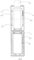
- a first embodiment of the present disclosure provides a film applicator, which is used to cooperate with the sticking film 200 to be pasted to the electronic product 300.
- the film applicator of this embodiment is a film-sticking box 10.
- the sticking film 200 includes a tempered film 201, a release film layer 202, a pulling portion 130 and a protective layer 240.
- the tempered film 201 is used to be pasted to the screen 301 of the electronic product 300.
- the release film layer 202 is attached to the tempered film 201, and the release film layer 202 is an electrostatic layer.
- the tempered film 201 has a sticking surface 2011 attached to the release film layer 202.
- the sticking surface 2011 is pasted to the screen 301 of the electronic product 300.
- the release film layer 202 and the tempered film 201 are separated when pasting, static electricity is generated on the side of the release film layer 202 attached to the tempered film 201, and the side with static electricity of the release film layer 202 is close to the screen 301 of the electronic product 300 to attract the dust on the screen.
- the release film layer 202 and the pulling portion 130 are integrally formed or separately arranged.
- the release film layer 202 and the pulling portion 130 need to be connected by means of pasting, clamping, etc.
- the pulling portion 130 is made of the same material as the release film layer 202, with the same thickness thereof. It can be understood that, in other embodiments, the pulling portion 130 only plays the role of pulling away the release film layer 202. In order to save the material for preparing the pulling portion 130, the thickness of the pulling portion 130 is less than instead of greater than that of the release film layer 202.
- the pulling portion 130 and one end of the release film layer 202 in the length direction are pasted to be fixed as a connection therebetween, and extend along the length direction of the release film layer 202.
- Part or all of the pulling portion 130 is positioned on the side of the release film layer 202 away from the sticking surface 2011, that is, the side of the release film layer 202 away from the tempered film 201 can be bent by a breaking line.
- the pulling portion 130 extends for a certain length along the length direction of the release film layer 202. In this case, the pulling portion 130 provides the user with a more convenient force for tearing off the release film layer 202, and the tempered film 201 will not be contaminated due to the fingers touching the tempered film 201 when the release film layer 202 is torn off.
- the pulling portion 130 is positioned at the side of the release film layer 202 away from the sticking surface 2011, and the pulling portion 130 is pulled toward the extending direction of the pulling portion 130. At this time, the pulling portion 130 is torn from the sticking surface 2011 in a folded manner, and the operation can be performed at the top of the screen 301, that is, the release film layer 202 can be torn off in a folded manner by pulling the pulling portion 130.
- the side with static electricity of the release film layer 202 can be in contact with the screen 301 naturally, so that the dust can be taken away, and the use of static electricity can be maximized.
- the pulling portion 130 is connected to one end portion of the release film layer 202 in the width direction.
- the pulling portion 130 extends for a certain length along the width direction of the release film layer 202.
- the end of the pulling portion 130 connected to the release film layer 202 is defined as a connecting end 2023, and the other end thereof is defined as a free end 2024.
- the extension length of the pulling portion 130 along the length direction is greater than the length of the release film layer 202, that is, the end portion of the free end 2024 is beyond the end portion of the opposite end of the end portion of the release film layer 202 connected to the connecting end 2023.
- the extension length of the pulling portion 130 along the width direction is greater than the width of the release film layer 202.
- the end portion of the free end 2024 extends beyond the end portion of the opposite end of the end portion of the release film layer 202 connected to the connecting end 2023.
- the sticking film 200 further includes a protective layer 240 disposed on the side of the tempered film 201 away from the sticking surface 2011.
- the protective layer 240 includes a covering portion 241 covering the tempered film 201, and a fixing portion 242 extending beyond the covering portion 241.
- the fixing portion 242 is provided with a positioning member 243 for cooperating with the film-sticking box 10 to position the sticking film 200.
- the positioning member 243 is a through-hole or a pillar.
- the positioning member 243 can also be arranged at other positions, such as two ends of the protective layer 240 in the width direction, as long as the positioning member 243 can adapt to the positioning structure of the film applicator.
- the pulling portion 130 is positioned between the release film layer 202 and the screen 301 of the electronic product 300, with a gap existed between the release film layer 202 and the screen 301.
- the thickness of the pulling portion 130 is equal to that of the release film layer 202, in order to smoothly pull the pulling portion 130 to move between the screen 301 and the release film layer 202, and smoothly pull the release film layer to be torn off, when the release film layer 202 is torn off, the release film layer 202 is positioned between the tempered film 201 and the screen 301 in a curved shape.
- the height of the gap therebetween at least needs to be greater than or equal to the thickness of the release film layer 202.
- the gap between the release film layer 202 and the screen 301 is compared with the thickness of the release film layer 202 to make the technical solution of the present disclosure clearer to those skilled in the art.
- the release film layer 202 can be torn off after the electronic product 300 is placed, so that the time interval between tearing off the release film layer 202 and pasting the tempered film 201 to the screen 301 is shorter, the operation steps are more consistent, and the time in contact with the air is shortened.
- the process of tearing off and pasting is carried out almost at the same time, which avoids attracting too much dust and improves the film-sticking effect.
- the release film layer 202 During the process of tearing off the release film layer 202, the release film layer 202 generates static electricity to attract the dust on the screen 301. That is, the release film layer 202 is torn off in a folded manner by pulling the pulling portion 130, so that the side with static electricity of the release film layer 202 can be in contact with the screen 301 naturally to attract the dust on the screen 301.
- the release film layer 202 is made of a material that is easy to generate static electricity by friction, so that static electricity can be generated when the release film layer 202 and the tempered film 201 are separated.
- the release film layer 202 is made of synthetic-resin-based material, rubber-based material or the like.
- the synthetic-resin-based material includes PET (polyethylene terephthalate), PE (polyethylene), PC (polycarbonate) or PVC (polyvinyl chloride).
- the rubber-based material includes SBR (styrene butadiene rubber), NBR (nitrile butadiene rubber), or some BR (butadiene rubber).
- PET is selected as the material for preparing the release film layer 202.
- the PET material has a wide source, low cost, and excellent material performance.
- the release film layer 202 can be prepared to have different hardnesses according to requirements, so as to prepare different types of the sticking film 200.
- the tempered film 201 has an impact-resisting function, and is mainly prepared by tempering a glass sample made of some silicate material.
- the main material and preparation process thereof are prior art, which will not be repeated here.
- the sticking surface 2011 of the tempered film 201 prepared based on a general process usually includes some glue, such as AB glue, OCA glue or some other polymerized organic compound. Therefore, some of the tempered films 201 easily generate static electricity when separated from the release film layer 202, which will easily cause the tempered film 201 to generate static electricity and attract the dust when the release film layer 202 is separated.
- some antistatic materials are added to make the tempered film 201 have antistatic properties, so that when the release film layer 202 is torn off from the tempered film 201, the tempered film 201 will not generate static electricity, which prevents the tempered film 201 from attracting dust and improves the cleanliness of the tempered film 201.
- Way 1 is that during the process of tearing off the release film layer 202, the release film layer 202 is close to instead of in contact with the screen 301, and the static electricity thereof is used to attract dust.
- the tempered film 201 will directly face the screen 301, and the dust on the screen 301 will easily fly to the sticking surface of the tempered film 201.
- Way 2 is that during the process of tearing off the release film layer 202, the release film layer 202 is curled between the screen 301 and the sticking surface 2011 of the tempered film 201, and the release film layer 202 falls on the screen 301 and contacts the screen 301. In this case, when torn off, the release film layer 202 first contacts the screen 301 to attract the dust, so as to prevent the dust from being adsorbed on the tempered film 201.
- the release film layer 202 is in contact with the screen 301, which can well prevent the dust on the area of the screen 301 not covered by the torn release film layer 202 from flying up under the electrostatic attraction of the tempered film 201 and the release film layer 202, resulting in the tempered film 201 also attracting dust.
- the tempered film 201 can be an antistatic layer or a non-antistatic layer.
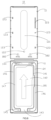
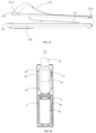
- the film-sticking box 10 includes a main body portion, which includes a base 11 and an upper cover 12, and the upper cover 12 includes a first end 151 and an opposite second end 152.
- the first end 151 is connected to the base 11, the upper cover 12 is closed on the second end 152, and a pulling opening 13 is formed by closing the upper cover 12 on the base.
- the upper cover 12 is recessed toward the base 11, and in the recessed area of the upper cover 12, the cross-section view of the upper cover cut by a direction perpendicular to the length direction of the upper cover 12 is in the shape of a concave arc.
- the curvature of the concave arc of the upper cover 12 gradually increases from the first end 151 to the second end 152.
- the middle area of the upper cover 12 in the direction from the first end 151 to the second end 152 is recessed.
- the upper cover 12 can be opened or closed, and manners of connecting the upper cover 12 and the base 11 are various.
- the upper cover 12 is rotatably connected to the base 11.
- One end between the first end 151 of the upper cover 12 and the base 11 is provided with a connecting member, which can be rotated, and by rotating the connecting member, the upper cover 12 can be rotated around the base 11 to be opened or closed.
- the connecting member may be a rotating shaft, or a flexible plastic, or the like.
- the upper cover 12 and the base 11 can also be hinged through hinges.
- the upper cover 12 and the base 11 can further be slidably connected.
- Guide rails or guide grooves are arranged on both sides of the base 11 in the length direction, and corresponding guide grooves or guide rails are arranged on both sides of the length direction of the upper cover 12, so that the upper cover 12 slides on the base 11 to close and open the upper cover 12.
- the release film layer 202 is provided with a pulling portion 130, which can pass through the pulling opening 13. The closer to the first end 151, the smaller the concave degree of the upper cover 12; the closer to the second end 152, the greater the concave degree of the upper cover 12.
- the recessed area of the upper cover 12 may extend continuously from the first end 151 to the second end 152, or may extend continuously from any position between the first end 151 and the second end 152 to the second end 152.
- the recessed area may also extend between any two positions from the first end 151 to the second end 152.
- the upper cover 12 and/or the end face opposite to the second end 152 of the base 11 are cut along the height direction to form a notch to define the pulling opening 13.
- the sticking film 200 When pasting, the sticking film 200 is placed in the film-sticking box 10, and the pulling portion 130 passes through the pulling opening 13.
- the height of the gap between the screen 301 and the release film layer 202 at the end with the less concave degree is equal to the thickness of the release film layer 202, and the end with less concave degree of the upper cover 12 is in contact with the sticking film 200, which also makes the sticking film 200 in contact with the screen 301. That is, the inner surface of the upper cover 12, the sticking film 200 and the screen 301 are in contact with each other in sequence.
- the concave upper cover 12 gives a pressure to the sticking film 200 so that the tempered film 201 can be pasted to the screen 301.
- the upper cover 12 has elasticity, and the pressure applied by the upper cover 12 to the sticking film 200 is a variable elastic force, which will not be too large to damage the screen 301 of the electronic product 300, but can also provide a suitable pressure to make the tempered film 201 attach to the screen 301 so that the generation of air bubbles is reduced or even no air bubbles are generated.
- the dislocation of the tempered film 201 and the screen 301 of the electronic product 300 due to incomplete attachment is prevented, which improves the film-sticking effect of the electronic product 300.
- the concave degree of the upper cover 12 close to the first end 151 is small, and the pressure applied by the upper cover 12 to the sticking film 200 is small, or even no pressure is applied, so that there is still a certain distance between the sticking film 200 and the screen 301, and the pulling portion 130 can be pulled easily.
- the concave degree of the upper cover 12 close to the second end 152 is large, and the pressure applied by the upper cover 12 to the sticking film 200 is large, and a larger frictional force can be generated between the release film layer 202 and the screen 301 so that the static electricity of the release film layer 202 can attract and take away the dust on the screen 301of the electronic product 300.
- the recessed area of the upper cover 12 extends to the second end 152 in the direction from the first end 151 to the second end 152, or extends from any position between the first end 151 and the second end 152 to the second end 152, and the upper side of the pulling opening 13 is in the shape of a downward concave arc.
- the pressure applied by the upper cover 12 to the sticking film 200 is the largest at the second end 152.
- the tempered film at the lower end that is, the tempered film 201 at the second end 152 is in contact with the screen 301 first, and then is gradually pasted to the screen 301 from this end to the direction of the first end 151, so that the direction of the film-sticking process is a fixed direction, and air bubbles can be discharged by the pressure to improve the quality of the film sticking.
- the concave arc of the upper cover 12 can be well formed by the preparation of the mold with the corresponding concave arc, or by the preparation of the film box 10 made of thermoplastic material, such as PP material. If the thickness of the upper cover 12 is set to a relatively thin size, and the relative middle portion is not provided with a structure for connecting with the base 11, there will be a cooling and shrinkage process in the cooling stage after the thermal injection molding is completed, so that a corresponding concave arc is naturally formed on the upper cover 12 after the cooling process.
- an observation window 121 is defined on the upper cover 12, which extends along the length direction of the upper cover 12.
- the observation window 121 includes a third end 153 close to the first end 151 of the upper cover 12 and a fourth end 154 close to the second end 152 of the upper cover 12.
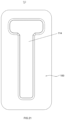
- the observation window 121 is arranged in a "1" shape in the length direction of the upper cover 12, or can also be arranged in other shapes, such as "T" shape, "Z” shape, "I” shape, etc.
- the upper cover 12 will be recessed toward the base 11 around the observation window 121 due to the structure of the film-sticking box 10 and the stress around the observation window 121.
- the shape of the observation window 121 is different, the stress around the observation window 121 is accordingly different, and the upper cover 12 will have different concave degrees around the observation window 121 toward the base 11.
- the observation window 121 is arranged in a "1" shape along the length direction of the upper cover 12.
- the arrangement of the observation window 121 also facilitates opening and closing the upper cover 12.
- the upper cover 12 can be easily opened by buckling the upper cover 12 at the observation window 121, and can be easily closed by buckling the upper cover 12 at the observation window 121 and pressing the upper cover 12.
- the arrangement of the observation window 121 also facilitates the separation of the sticking film 200 and the upper cover 12.
- the sticking film 200 is fixed on the inner side of the upper cover 12. When the sticking film 200 and the upper cover 12 needs to be separated, the upper cover 12 and the sticking film 200 can be easily separated by directly pushing the sticking film 200 through the observation window 121 on the outer side of the upper cover 12.
- the distance between the third end 153 and the first end 151 is defined as S1
- the distance between the fourth end 154 and the second end 152 is defined as S2, and S1>S2.
- the observation window 121 is arranged in a "1" shape along the length direction of the upper cover 12, and the distance between the third end 153 and the first end 151 is greater than the distance between the fourth end 154 and the second end 152. Since S2 ⁇ S1, the stress of the observation window 121 is larger at the position close to the fourth end 154, while the stress is smaller at the position close to the third end 153; the concave degree of the upper cover 12 is larger at the position close to the fourth end 154, while the concave degree is smaller at the position close to the third end 153. In the concave area of the upper cover 12, the curvature of the concave arc of the upper cover 12 gradually increases from the third end 153 to the fourth end 154 in the direction from the first end 151 to the second end 152.
- a first midpoint P1 is defined on the outer surface of the upper cover 12, which is arranged at the midpoint of the edge of the first end 151 of the outer surface of the upper cover 12, and the distance between the first midpoint P1 and the base 11 is defined as L1;
- a second midpoint P2 is defined on the outer surface of the upper cover 12, which is arranged at the midpoint of the edge of the second end 152 of the outer surface of the upper cover 12, and the distance between the second midpoint P2 and the base 11 is defined as L2, and L1>L2.
- the upper cover 12 has a downward slope from the first end 151 to the second end 152, and the concave degree of the upper cover 12 gradually increases from the first end 151 to the second end 152 in the direction from the first end 151 to the second end 152.
- the first midpoint P1 is arranged at the midpoint of the edge of the first end 151 of the outer surface of the upper cover 12, and the distance between the first midpoint P1 and the base 11 is defined as L1;
- the second midpoint P2 is arranged at the midpoint of the edge of the second end 152 of the outer surface of the upper cover 12, and the distance between the second midpoint P2 and the base 11 is defined as L2.
- L1 and L2 have the following relationship: L1>L2, and 1mm ⁇ L1-L2 ⁇ 3mm. When the base 11 of the film-sticking box 10 is laid flat, the first midpoint P1 is 1-3 mm higher than the second midpoint P2.
- the curvature of concave arc of the upper cover 12 gradually increases in the direction from the first end 151 to the second end 152.
- the curvature of the concave arc of the upper cover 12 is the smallest at the first end 151 and is the largest at the second end 152.
- the inner side of the upper cover 12 is provided with a sticking region 122, which is arranged at any position that can be covered by the sticking film 200, and the area of the sticking region 122 is not limited, as long as the sticking region 122 can adhere the sticking film 200 to the sticking region 122.
- the area of the sticking region 122 may be set to 2-5cm2.
- the sticking region 122 can be coated with an adhesive, or can be adhered with a double-sided adhesive tape, or other methods for adhering the sticking film 200 to the inner side of the upper cover 12, which are not limited herein.
- the sticking region 122 is arranged next to the observation window 121 at the end of the concave arc with a smaller curvature.
- the sticking region 122 is pasted with an unused double-sided adhesive tape, and the protective paper layer of the double-sided adhesive tape can prevent the sticking film 200 from adhering to the upper cover 12 in advance, and can prevent the adhesive layer of the sticking region 122 from being exposed and losing its adhesiveness, which may reduce the adhesive effect.
- the protective paper layer of the double-sided adhesive tape is torn off, the sticking film 200 is fixed on the inner side of the upper cover 12, and the release film layer 202 is adhered by the double-sided adhesive tape.
- the pulling portion 130 When the pulling portion 130 is pulled, the tempered film 201 is pasted to the screen 301 of the electronic product 300, the pulling portion 130 is separated from the tempered film 201, and the release film layer 202 remains on the upper cover 12. There is no need to manually separate the release film layer 202 and the tempered film 201, which reduces the operation steps of film sticking, and is convenient and quick.
- the inner side of the upper cover 12 is provided with a plurality of fixing portions 123, which are arranged inside the upper cover 12, and are arranged on two opposite sides of the upper cover 12 in the length direction of the upper cover 12.
- the fixing portion 123 cooperates with the positioning member 243 of the sticking film 200 to fix the sticking film 200 on the inner side of the upper cover 12, which ensures the consistency of the positions of the sticking film 200 and the screen 301 of the electronic product 300, so that when the film is pasted, the sticking film 200 and the screen 301 of the electronic product 300 will not be displaced.
- the fixing portion 123 may have various shapes, such as a convex cylindrical shape, a convex elongated shape, a square shape, a diamond shape, etc.
- the shapes of the fixing portions 123 arranged on one side and on the other side of the upper cover 12 may be different, even the shapes of the fixing portions 123 on the same side of the upper cover 12 may be different.
- the three short-strip-shaped fixing portions 123 are sequentially arranged on one side of the upper cover 12, and the shapes of the fixing portions 123 sequentially arranged at the other side of the upper cover 12 are respectively the shape of elongated bar, short bar and cylinder.
- the obvious cylindrical or elongated fixing portion 123 is selected to facilitate the user to clearly distinguish the front and rear sequence of the sticking film 200, and to position and install the sticking film 200 quickly and accurately.
- the fixing portions 123 are arranged at two opposite side edges of the upper cover 12, the strength of the edges on both sides of the upper cover 12 can be well strengthened, so that when the upper cover 12 is prepared, the middle position of the upper cover 12 can be well recessed.
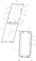
- the film-sticking box 10 further includes a substrate 14, which is mounted on the base 11 and is provided with a mounting slot 141.
- the shape and size of the mounting slot 141 are configured according to specific electronic product models, since different electronic product models have different positions of the volume key and the power key.
- an empty space can be left at the positions of the volume key and the power key.
- the electronic product 300 is placed in the mounting slot 141 to be fixed in the film-sticking box 10, and will not be displaced or shaken, and the dislocation of the sticking film 200 and the screen 301 of the electronic product 300 is prevented, thereby improving the film-sticking effect of the electronic product 300.
- the substrate 14 is further provided with a positioning pin 162, and the base 11 is provided with a corresponding positioning hole 161.
- the bottom of the substrate 14 is provided with a plurality of positioning pins 162, and the number and position of the positioning pins 162 are generally not limited.
- four positioning pins 162 may be arranged in four directions of the substrate 14 and distributed in a rectangular shape on the substrate 14.
- four positioning holes 161 are protruded on the base 11, and the four positioning holes 161 are arranged in four directions of the base 11 and distributed in a rectangular shape on the base 11.
- the positioning holes 161 correspond to the positioning pins 162 respectively, with the same number, corresponding positions, and matching sizes.
- the positioning pins 162 can be inserted into the positioning holes 161 without displacement or shaking.
- the substrate 14 is detachably mounted on the base 11. When pasting, the substrate 14 is mounted on the base 11, the electronic product 300 is placed on the substrate 14, and the electronic product 300 is fixed in the film-sticking box 10, so that the electronic product 300 will not be displaced or shaken, which prevents the dislocation of the sticking film 200 and the screen 301 of the electronic product 300, and improves the film-sticking effect of the electronic product 300.
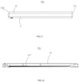
- the substrate 14 includes a first end wall 144 and an opposite second end wall 145, and two side walls 146 arranged between the first end wall 144 and the second end wall 145.
- the first end wall 144, the second end wall 145 and the two side walls 146 define the mounting slot 141, and the inner positions of the first end wall 144, the second end wall 145 and the side walls 146 are provided with supporting edges 147 to support the electronic product 300.
- the substrate 14 further defines an accommodating slot 142, which is arranged below and communicates with the mounting slot 141.
- an accommodating slot 142 is arranged below and communicates with the mounting slot 141.
- a camera is protruded from the back of the electronic product 300, and the camera and the back of the electronic product 300 are not on the same plane, which may cause the electronic product 300 to be unstable.
- the accommodating slot 142 below the mounting slot 141, the camera is accommodated in the accommodating slot 142, and the electronic product 300 can be smoothly mounted in the mounting slot 141, which further ensures the stability of the electronic product 300 and the film-sticking effect of the electronic product 300.
- the position of the accommodating slot 142 can be configured at different positions according to different models of electronic products and different positions of cameras.
- the substrate 14 further defines a groove 143, which is communicated with the mounting slot 141.
- the groove 143 is disposed on the first end wall 144 or the second end wall 145, and the groove bottom of the groove 143 and the slot bottom of the mounting slot 141 are on the same plane.
- the shape of the groove 143 is not limited, and the size of the groove 143 can accommodate a finger of an adult.
- the arrangement of the groove 143 is convenient for placing the electronic product 300 in and taking the electronic product 300 out of the mounting slot 141.
- the electronic product 300 can be placed in or taken out by holding the electronic product 300 with fingers at the groove 143, which is convenient and quick.
- the upper cover 12 and the base 11 are clamped at the second end 152. Both sides of the base 11 in the width direction are provided with clamping slots 171, and the upper cover 12 is provided with clamping buckles 172 corresponding to the clamping slots 171 on both sides of the second end 152 in the width direction. The upper cover 12 and the base 11 are clamped at the second end 152 through the cooperation of the clamping slot 171 and the clamping buckle 172.
- the upper cover 12 and the base 11 are relatively fixed, and the upper cover 12 will not shake, which ensures the stability of each component, and prevents the dislocation of the sticking film 200 and the screen 301 of the electronic product 300, thereby improving the film-sticking effect of the electronic product 300.
- the pulling opening 13 is formed at the middle portion between the upper cover 12 and the second end 152 of the base 11. Since the clamping buckles 172 are arranged at the edge positions of both sides of the upper cover 12, the formation of the pulling opening 13 is not affected.
- the strength of the edges on both sides of the second end 152 of the upper cover 12 can be well strengthened, so that when the upper cover 12 is prepared, the middle position of the second end 152 of the upper cover 12 is recessed. Due to the large deformation of the second end 152, the user can press the second end 152 during the process of sticking to make the tempered film 201 to be pasted to the screen 301 of the electronic product 300.
- the film-sticking box 10 is provided with indication marks, which include a first indication mark 181, a second indication mark 182 and a third indication mark 183.
- the first indication mark 181 is disposed on the inner side of the base 11, points from the end close to the pulling opening 13 to the end away from the pulling opening 13, and is used to indicate the placement direction of the electronic product 300.
- the second indication mark 182 is disposed on the inner side of the upper cover 12, is close to the first end 151, points from the second end 152 to the first end 151, and is used to indicate the installation direction of the sticking film 200.
- the use of the second indication mark 182 in cooperation with the fixing portion 123 can increase the user's recognition of the direction of the film-sticking box 10, so that the user can quickly and accurately fix the sticking film 200 on the upper cover 12.
- the third indication mark 183 is disposed on the outer side of the upper cover 12 away from the base 11, is close to the second end 152, points from the first end 151 to the second end 152, and is used to indicate the opening and closed position of the film-sticking box 10.
- the first indication mark 181, the second indication mark 182 and the third indication mark 183 are concave indication arrows, and the indication marks will not become blurred due to wear and tear even if used for many times.
- the first indication mark 181, the second indication mark 182 and the third indication mark 183 may also be protruded indication arrows, and may also be indication arrows drawn in color or text descriptions, etc.
- the material of the film-sticking box 10 is not limited, and can be made of polymer or metal.
- the film-sticking box 10 is made of plastic.
- Plastics are polymer compounds that are polymerized from monomers through polyaddition or polycondensation. Plastic is light in weight, easy to transport and use; plastic has good transparency and wear resistance, is not easy to wear, and has a long lifetime; plastic has good formability, good colorability, is easy to process and has low processing cost; plastic has a certain elasticity, can perform elastic deformation, which is more convenient for the upper cover 12 to be recessed.
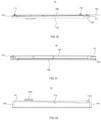
- a second embodiment of the present disclosure provides another film-sticking box 10a, which is different from the film-sticking box 10 of the first embodiment mainly in that the upper cover 12 is not recessed, instead, the inner surface of the upper cover 12 is configured to be inclined relative to the horizontal plane (the dotted line is horizontal relative to the horizontal plane), and the height of the inner surface of the upper cover 12 relative to the horizontal plane gradually decreases from the first end 151 to the second end 152 in the length direction of the upper cover 12.
- the supporting edge 147 is horizontal relative to the horizontal plane.
- the height of the inner surface of the upper cover 12 relative to the horizontal plane can also gradually decrease from the first end 151 to the second end 152 in the width direction of the upper cover 12, and the supporting edge 147 is horizontal relative to the horizontal plane.
- a third embodiment of the present disclosure provides another film-sticking box 10b.
- the inner surface of the upper cover 12 for fixing the sticking film 200 is at the same height relative to the horizontal plane, and the supporting edge 147 is inclined relative to the horizontal plane (the dotted line is horizontal relative to the horizontal plane).
- the height relative to the horizontal plane gradually increases from the first end 151 to the second end 152, and the tempered film 201 is horizontal relative to the horizontal plane.
- the height of the tempered film 201 close to the second end 152 relative to the screen 301 is lower than the height of the tempered film 201 close to the first end 151 relative to the screen 301.
- the pulling portion 130 at the lower-concave end of the upper cover 12, or at the lower end of the tempered film 201 relative to the horizontal plane is not in contact with the screen 301.
- the sticking film 200 After the sticking film 200 is positioned, there is a certain spatial distance between the sticking film 200 and the screen 301, that is, the distance between the release film layer 202 and the screen 301 is greater than the thickness of the release film layer 202.
- the release film layer 202 is torn off, the release film layer 202 is positioned between the tempered film 201 and the screen 301 in a curved shape.
- the distance L between the screen 301 and the release film layer 202 is equal to 3-300 times the thickness of the release film layer 202.
- the range of the distance L may also be 5 times, 15 times, 30 times, 50 times, 80 times, 130 times, 200 times, or 250 times the thickness of the release film layer 202.
- the distance L is equal to 100-300 times the thickness of the release film layer 202.
- the range of the distance L may also be 115 times, 125 times, 130 times, 150 times, 180 times, 200 times, 220 times, or 250 times the thickness of the release film layer 202.
- the side of the release film layer 202 in contact with the sticking surface 2011 is configured to be in natural contact with the screen 301, so that the release film layer 202 and the screen 301 can directly attract these fine dusts and the cleaning ability can be improved.
- the distance L is equal to 3-100 times the thickness of the release film layer 202.
- the range of the distance L may also be 10 times, 30 times, 50 times, 70 times, 80 times or 90 times the thickness of the release film layer 202.
- the concave upper cover 12 is provided; in the film-sticking box 10a of the second embodiment, the upper cover 12 is configured with an inclined structure; in the film-sticking box 10b of the third embodiment, the supporting edge 147 on the base 14 is configured at an inclined angle, so that the distance between the tempered film 201 on the side close to the pulling opening 13 and the screen 301 is relatively low, and the distance between the tempered film 201 on the side away from the pulling opening 13 and the screen 301 is relatively high.
- the tempered film 201 on the lower side is in contact with the screen 301 first, and then the tempered film 201 is attached from this end to the opposite end.
- the direction of the film is well controlled, so that the direction of the film pasting is in a fixed direction, which is conducive to taking away the air bubbles and improving the quality of the film pasting. That is, the direction of tearing off the release film layer 202 is carried out from the first end 151 to the second end 152, the film pasting is applied from the second end 152 to the first end 151, which means the directions of tearing and sticking are opposite.
- the tempered film 201 on the side close to the pulling opening 13 is configured at a higher height relative to the screen 301, and the tempered film 201 on the side away from the pulling opening 13 is configured at a lower height relative to the screen 301.
- This configuration is also possible, as long as a height difference can be formed to ensure that the air bubbles are discharged in one direction.
- the direction of tearing off the release film layer 202 is from the first end 151 to the second end 152, and the film sticking is also carried out in the direction from the first end 151 to the second end 152, which means the directions of tearing and sticking are the same.
- the tempered film 201 at this end can be pressed to contact the screen 301 to realize the film sticking, that is, the effect of tearing and sticking can be realized almost simultaneously, which can prevent dust from entering the screen 301 better.
- another film-sticking box 60 is provided.
- the upper cover 12 is arranged horizontally relative to the horizontal plane, and the substrate 14 is also arranged horizontally relative to the horizontal plane.
- the height of the tempered film 201 relative to the surface of the screen 301 is the same, and there is no inclination angle, as long as the height of the tempered film 201 relative to the screen 301 is controlled within a suitable range to ensure that the tempered film 201 can be aligned and pasted to the screen 301 after the release film layer 202 is torn off.
- the height of the tempered film 201 relative to the surface of the screen 301 ranges from 3-300 times the thickness of the release film layer 202.
- an optional film-pasting process includes steps of:
- a fifth embodiment of the present disclosure provides another film applicator 40, which is used to cooperate with the sticking film 200 of the first embodiment to be pasted to an electronic product.
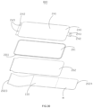
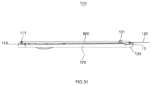
- the film applicator 40 includes a main body portion, which includes a substrate 41 with a first end wall 110 and an opposite second end wall 120 in the length direction and two side walls 170 between the first end wall 110 and the second end wall 120.
- the first end wall 110, the second end wall 120 and the two side walls 170 form a mounting slot 42 for accommodating and mounting the electronic product.
- the substrate 41 further includes a fixing portion, which includes a first fixing portion 111 arranged on the first end wall 110 and a second fixing portion 131 arranged on the side wall 170.
- the height of the second end wall 120 is lower than the height of the first end wall 110 to form the pulling opening 13, so that when the protective layer 240 of the sticking film 200 is positioned on the first fixing portion 111 and the second fixing portion 131, the pulling portion 130 of the release film layer 202 of the sticking film 200 can cross the upper end face of the second end wall 120 and extends outwards for the user to pull.
- the frictional resistance when the release film layer 202 is pulled can be reduced.
- the height difference between the first end wall 110 and the second end wall 120 is greater than or equal to the thickness of the sticking film 200, the best effect of reducing frictional resistance can be achieved, since the pressure between the pulling portion 130 and the second end wall 120 is the smallest at this time. Therefore, making the second end wall 120 lower than the first end wall 110 can ensure the release film layer 202 to be torn off by dragging the pulling portion 130 after the sticking film 200 is positioned.
- the second end wall 120 can leave a moving space for the pulling portion 130 of the release film layer 202, so that when the the release film layer 202 is torn off, the time that the sticking surface of the sticking film 200 is exposed to the air is greatly reduced, thereby reducing the probability that the sticking surface of the sticking film 200 is contaminated with dust, and improving the sticking effect and dustproof effect.
- the first fixing portion 111 includes a plurality of first positioning pillars 111a, and the first positioning pillar 111a close to one of the side wall 170 is configured as a fool-proof positioning pillar 111b.
- the cross-sectional shape and/or the size of the fool-proof positioning pillar 111b is different from that of the other first positioning posts 111a.
- the above configuration is to prevent the user from mistaking the front and back sides of the sticking film 200. Since the cross-sectional shapes of the fool-proof positioning pillar 111b and the first positioning pillar 111a are different, the first fixing portion 111 does not have an axis of symmetry parallel to the extending direction of the side wall 170. If the user rotates the sticking film 200 by 180 degree with the extension direction of the side wall 170 as the axis, the positioning member 243 is made a symmetrical transformation according to the axis.
- the positioning member 243 cannot be positioned on the first fixing portion 111 at this time, and the user can know that the front and back of the sticking film 200 are reversed.
- the fool-proof positioning pillar 111b may not be provided, and it is only necessary that the first fixing portion 111 does not have an axis of symmetry parallel to the extending direction of the side wall 170, for example, the three first positioning pillars 111a are arranged on the same straight line at unequal intervals.
- the cross-section of the fool-proof positioning pillar 111b is rectangular, and the cross-section of the other first positioning pillars 111a is circular.
- This solution further refines the method that the first fixing portion 111 does not have an axis of symmetry parallel to the extending direction of the side wall 170.
- the cross-section of the fool-proof positioning post 111b is rectangular, so that the geometric shapes of the fool-proof positioning post 111b and the other first positioning pillars 111a are different, and the user can quickly determine the front and rear position of the sticking film 200.
- the fool-proof positioning pillar 111b is not provided, although the three first positioning pillars 111a with the same geometric shape distributed on the first end wall 110 at unequal intervals can also play the role of distinguishing the front and rear of the sticking film 200, compared with the solution with the fool-proof positioning pillar 111b, the distinction between the front and rear is less obvious.
- the cross-section of the fool-proof positioning pillar 111b may also be in other shapes different from that of the first positioning pillar 111a.
- the cross-section of the first positioning pillar 111a is circular, and the cross-section of the fool-proof positioning pillar 111b is oval; the cross-section of the first positioning pillar 111a is square, and the cross-section of the fool-proof positioning pillar 111b is triangular.
- the second fixing portion 131 includes a second positioning pillar 131 disposed close to the second end wall 120.
- the tearing force should be perpendicular to the extending direction of the first end wall 110, so that even only the first fixing portion 111 is sufficient to position the protective layer 240 well.
- the tearing force may not be perpendicular to the extending direction of the first end wall 110.
- the force on the sticking film 200 is not zero relative to the torque of the normal line of the upper end face of the first end wall 110 passing through the midpoint of the extending direction thereof, which will cause the torque of the sticking film 200 to be too large relative to the normal line, and cause the sticking film 200 to be distorted and deformed, destroying the positioning relationship between the protective layer 240 and the "first fixing portion 111 and the second fixing portion 131", causing the positioning to fail.
- the arrangement of the second fixing portion 131 can solve this problem. Since the second fixing portion 131 is on the side wall 170, when the sticking film 200 has a tendency of rotating, the second fixing portion 131 can give the protective layer 240 a torque that prevents the rotation of the sticking film 200.
- the height of the side wall 170 ranges from the height of the first end wall 110 to the height of the second end wall 120. If the height of the side wall 170 is greater than that of the first end wall 110, after the protective layer 240 is positioned on the first fixing portion 111 and the second fixing portion 131, since the second fixing portion 131 is positioned on the side wall 170, the overall highest height of the sticking film 200 is equal to the height of the side wall 170, and the highest height of the sticking film 200 is greater than that of the first end wall 110 in this case.
- the positioning member 243 cooperated with the first fixing portion 111 is not inserted into the bottom of the first positioning pillar 111a, and such a cooperation method is less reliable. If the height of the side wall 170 is lower than that of the second end wall 120, the lowest point of the sticking film 200 is lower than the height of the second end wall 120. In this case, the pulling portion 130 and the second end wall 120 will have pressure, which makes it inconvenient to tear off the release film layer 202.
- a transition slope 133 is provided between the upper end face of the side wall 170 and the upper end face of the second end wall 120.
- the height of the side wall 170 is greater than that of the second end wall 120, so the transition slope 133 can be provided to make a smooth transition between the side wall 170 and the second end wall 120.
- all the planes on the substrate are smoothly transitioned, so that the surface of the electronic product will not be scratched due to the sharp edges and corners of the film applicator 40 during the installation or removal process, and user's hands will not be scratched while using.
- the upper end face of the first end wall 110 defines an avoidance step 112 on the side close to the second end wall 120 to provide space for the connection between the release film layer 202 and the pulling portion 130. Since the release film layer 202 needs to be torn off after the sticking film 200 is positioned on the first fixing portion 111 and the second fixing portion 131, the adhesive strength between the release film layer 202 and the tempered film 201 should not be too large, which makes that if the initial end of the pulling portion 130 is on the edge of the sticking film 200, the release film layer 202 will be torn off easily. Therefore, the initial end of the pulling portion 130 is a certain distance away from the edge of the sticking film 200.
- the first end wall 110 does not define the avoidance step 112
- the first end wall 110 and the pulling portion 130 will be under pressure, which increases the resistance to tearing off the release film layer 202.
- the height of the avoidance step 112 should not be greater than the height of the screen of the electronic product accommodated in the mounting slot 42, so as to ensure sufficient avoidance.
- the height difference between the upper end face of the first end wall 110 and the avoidance step 112 should be greater than or equal to the sum of the thicknesses of the protective film 220 and the release film layer 202, so that the protective layer 240 does not squeeze the pulling portion 130 to increase the resistance when the release film layer 202 is torn off.
- the bottom of the mounting slot 42 is provided with an annular supporting edge 140.
- annular supporting edge 140 at the bottom of the mounting slot 42 can increase the thickness of the mounting slot 42 in the plane direction, so that the mounting slot 42 is not easily deformed when subjected to a force on the same plane as the mounting slot 42. If the mounting slot 42 is deformed, the electronic product cannot be normally accommodated and mounted.
- the supporting edge 140 can also play a role in limiting the position of the electronic product. When the electronic product is accommodated and mounted in the mounting slot 42, the back of the electronic product abuts against the supporting edge 140, so that the electronic product does not sink excessively, and the relative position between the mounting slot 42 and the electronic product remains unchanged.
- the inner side of at least one of the first end wall 110, the side wall 170 and the second end wall 120 is provided with an avoidance groove 132, which is used to accommodate the side buttons of the electronic product.
- Electronic products have side buttons, which protrude from the side of the device. If there is no avoidance groove 132, the mounting slot directly abuts with the side buttons of the electronic product to achieve the effect of positioning the electronic product. After the additional avoidance groove 132 accommodates the side buttons, the mounting slot abuts against the side of the electronic product without buttons to achieve the effect of positioning the electronic product.
- the pulling opening 13 can also be formed on the first end wall 110 or the side wall 170.
- the first end wall 110, the second end wall 120 and the two side walls 170 support the sticking film, and the pulling portion 130 overlaps the upper surface of the first end wall 110 or one of the two side walls 170 that forms the pulling opening 13.
- the inner surfaces of the first end wall 110, the second end wall 120 and the two side walls 170 are provided with protrusions 160, which are connected with the side surfaces of the electronic product.
- the contact of the protrusion 160 and the outer surface of the electronic product is changed from surface contact to point contact, which reduces the contact area between the film applicator 40 and the side wall 170 of the electronic product, reduces the possibility of being damaged by friction, and protects the electronic product.
- the material of the substrate 41 can be, but not limited to, paper, wood, degradable plastic, metal, ceramic, or non-degradable plastic.
- the substrate 41 is made of degradable plastic.
- a sixth embodiment of the present disclosure provides a film applicator 40a, which is different from the film applicator 40 of the fifth embodiment in that the side wall 170 has an inclined angle relative to the horizontal plane, the height of the side wall relative to the horizontal plane gradually increases from the first end wall 110 to the second end wall 120, and the heights of the first end wall 110 and the second end wall 120 are equal.
- the first fixing portion 111 is arranged on the first end wall 110
- the second fixing portion 131 is arranged on the two side walls 170
- the pulling opening 13 is formed on the second end wall 120.
- the sticking film 200 is positioned on the upper surfaces of the first end wall 110 and the two side walls 170, the first end wall 110 and the two side walls 170 support the sticking film 200, and the side wall 170 at the end with a higher height from the horizontal plane raises the sticking film 200, so that there is a certain distance between the sticking film 200 and the screen of the electronic device to form the pulling opening 13 for the pulling portion 130 to extend.
- a seventh embodiment of the present disclosure provides a film applicator 40b, which is different from the film applicator 40a of the sixth embodiment in that the two side walls 170 are horizontally arranged relative to the horizontal plane, and the height of the support edge 140 relative to the horizontal plane decreases from the first end wall 110 to the second end wall 120.
- the two side walls 170 are at the same height from the horizontal plane, and the pulling opening 13 is formed on the second end wall 120, after positioning the sticking film 200, there is a height difference between one end of the release film layer 202 relative to the electronic device and the other end of the release film layer 202 relative to the electronic device.
- an eighth embodiment of the present disclosure provides a film applicator 40c, which is different from the the film applicator 40 of the fifth embodiment mainly in that the difference in the materials for preparing the film applicator 40c. Based on the difference of materials, the sizes of the first end wall 110, the second end wall 120, and the side wall 170 are further set relatively large to ensure smooth demolding and improve the strength thereof.
- the upper end face of the side wall 170 is gradually inclined upward from the upper end face of the first end wall 110 toward the upper end face of the second end wall 120.
- the upper end faces of the first end wall 110 and the second end wall 120 are a flat surface or an extension surface of the upper end face of the side wall 170.
- the dashed-dotted line is a reference line parallel to the lower end face of the side wall 170, and the inclined form of the upper end face of the side wall 170 can be seen.
- the inclination of the side wall 170 may be much smaller than the inclination shown in the figure, since the thickness of the sticking film 200 is very small relative to the distance between the first end wall 110 and the second end wall 120.
- the height difference between the height of the first end wall 110 and the height of the second end wall 120 only needs to be greater than or equal to the thickness of the sticking film 200, so that a moving space can be reserved for the pulling portion 130. That is, there is a distance between the screen and the release film layer 202.
- the upper end face is an inclined surface connecting the upper end face of the first end wall 110 and the upper end face of the second end wall 120, and the tangent value of the inclination angle of the upper end face of the side wall 170 is at least equal to the thickness of the sticking film 200 divided by the distance between the first end wall 110 and the second end wall 120, which can be seen that this is a small angle.
- the beneficial effect of this arrangement is that the integrity of the substrate 41 is improved. If the substrate 41 is produced by a stamping method, it is beneficial to improve the success rate of stamping; if the substrate 41 is produced by an injection molding method, it is beneficial to improve the simplicity of mold manufacturing.
- the second end wall 120 includes a pulling slot 150, which prevents the second end wall 120 from abutting against the electronic product at the position of the pulling slot 150.
- a portion of the side of the electronic product is accessible to the user.
- the electronic product can be taken out from the mounting slot 42 by pulling the portion of the electronic product. Without the pulling slot 150, the electronic product needs to be poured out of the mounting slot 42, which may easily cause the electronic product to fall. Therefore, the pulling slot 150 increases the convenience and safety when taking out the electronic product.
- the second fixing portion 131 disposed on the side wall 170 and close to the pulling opening 13 is movably matched with the positioning member 243, and first fixing portion 111 disposed on the first end wall 110 is closely matched with the positioning member 243.
- the sticking film can be well pre-positioned on the first end wall 110, and then the sticking film can be further positioned by aligning with the second fixing portion 131.
- the sticking film can be well positioned while aligning, and a reasonable error caused by the sticking film or the film applicator 40 in the preparation process is allowed, which reduces the precision requirement of the preparation process.
- the material of the substrate 41 of the film applicator 40c is paper.
- paper, wood or degradable plastic after the substrate 41 is discarded, it can be quickly decomposed into small molecular substances in nature, returning to the carbon cycle of the earth, avoiding the waste of resources, and avoiding the ecological damage caused by the accidental eating of artificial objects by wild animals.
- the use of degradable materials such as paper has low cost and simple processing, which is more conducive to reducing production costs.
- the structure will not change, so the substrate can be reused, which further increases the environmental protection property of the substrate.
- the bottom of the mounting slot 42 in FIG. 15 is provided with the annular supporting edge 140 to increase the strength of the substrate 41, while the bottom of the mounting slot 42 in FIG. 16 is a closed structure, which is because the substrate 41 in FIG. 15 is made of degradable plastic, the material itself has high strength, and the strength of the base 41 only needs to be supplemented by the annular support edge 140; while the substrate 41 in FIG. 19 is made of paper, the material strength is low, and the slot bottom is configured as a closed structure to ensure the strength thereof.
- the substrate 41 in FIG. 15 is injection-molded, and the slot bottom is not closed, which can save materials and reduce costs; the substrate 41 in FIG. 19 is formed by stamping, and the material itself is closed. If the bottom of the slot is to be hollow, a shearing step needs to be added, which is the reason that the closed structure is configured to save the manufacturing cost.
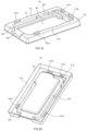
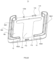
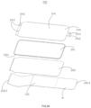
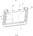
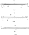
- a ninth embodiment of the present disclosure provides a film applicator 50, which includes a main body portion provided with a substrate 100.
- the substrate 100 includes a connecting plate 501, a positioning edge 502 and a fixing portion 112 that are arranged on the same surface of the connecting plate 501.
- the positioning edge 502 forms a mounting slot 180 that is used for positioning the electronic product and the sticking film 200.
- the side wall of the mounting slot 180 is provided with a pulling opening 13 that is used for passing through the puling portion 130 on the release film layer 202 of the sticking film 200.
- the mounting slot 180 is provided on the substrate 100.
- the sticking film 200 is first installed on the bottom of the mounting slot 180, so that the release film layer 202 of the sticking film 200 faces the notch of the mounting slot 180, then insert the pulling portion 130 through the pulling opening 13, and then install the electronic product into the mounting slot 180 of the substrate 100 in the direction that the screen of the electronic product faces the sticking film 200, finally pull the pulling portion 130 to tear off the release film layer 202 from the tempered film 201, and attach the tempered film 201 to the screen of the electronic product.
- the sticking film 200 and the mounting slot 180 Since the film-sticking process of the electronic product is carried out in a sealed environment formed by the electronic product, the sticking film 200 and the mounting slot 180, it can effectively prevent impurities such as dust in the air from entering the screen of the electronic product, thereby preventing the generation of air bubbles between the tempered film 201 and the screen due to the existence of impurities.
- the sticking film 200 and the electronic product are installed in the mounting slot 180 simultaneously, so that the screen of the sticking film 200 and the electronic product can be automatically aligned, so as to prevent the dislocation of the sticking film 200 and the screen of the electronic product.
- the film applicator 50 can be reused, if the sticking film 200 is damaged during use, users can just buy the sticking film 200 and install it in the film applicator 50 to perform the sticking operation, without repurchasing a new film applicator 50. It can be seen that the technical solution of the present disclosure is not only simple to operate and has a higher performance, but can also improve the film-sticking effect and dust-removal effect of electronic products, and the film applicator can be reused.
- the electronic product may be a pad, a mobile phone, a watch, or the like, and the type of the electronic product is not specifically limited here.
- the positioning edge 502 includes two opposite first positioning edges 5021 and two opposite second positioning edges 5022, and the two first positioning edges 5021 and the two second positioning edges 5022 are connected end to end to define the mounting slot 180.
- the connecting plate 501 includes a first side and a second side in the length direction or in the width direction thereof, the first positioning edges 5021 are arranged on both sides of the connecting plate 501 in the length direction thereof, and the second positioning edges 5022 are arranged on one side of the connecting plate 501 in the width direction thereof.
- Each of the second positioning edges 5022 is connected to the end of one of the first positioning edges 5021.
- the two second positioning edges 5022 are oppositely arranged with a certain interval therebetween to form the notch 113.
- the notch 113 is also formed at the other end opposite to the second positioning edge 5022 since the second positioning edge 5022 is not provided.
- the second positioning edge 5022 is formed by the end of the first positioning edge 5021 extending a distance along the width direction of the connecting plate 501.
- the pulling opening 13 is disposed at the bottom of the side wall of the slot. That is, the pulling opening 13 is disposed at the connection between the second positioning edge 5022 and the connecting plate 501.
- the pulling portion 13 can be formed by cutting off part of the second positioning edge 5022 to form a gap existed between the second positioning edge 5022 and the surface of the connecting plate 501.
- the sticking film 200 is installed at the bottom of the mounting slot 180, and the pulling opening 13 is arranged at the bottom of the side wall of the slot, which can make the release film layer 202 of the sticking film 200 straight out of the substrate 100, so as to prevent the dislocation of the sticking film 200 caused by the deflection of the release film layer.
- the pulling opening 13 may also be disposed on the edge of the bottom wall of the slot.
- the edge of the mounting slot 180 is provided with a positioning structure, which is used for the positioning and installation of the protective layer 240 of the sticking film 200.
- the positioning structure is to match the positioning portion on the protective layer 240 of the sticking film 200 to position the sticking film 200, which prevents the sticking film 200 from being displacement relative to the screen of the electronic product, and achieves precise positioning of the components of the sticking film 200 to prevent the sticking film 200 from being damaged.
- the positioning structure includes a plurality of fixing portions 112, and each of the opposite sides of the mounting slot 180 is provided with a portion of the fixing portions 112. That is, the fixing portions 112 are arranged at the positions of the two notches 113. At least one fixing portion 112 is configured as a fool-proof convex portion 112a, and the cross-sectional size and/or the shape thereof is different from that of the other fixing portions 112. Specifically, the protective layer 240 of the sticking film 200 is also provided with positioning holes and fool-proof hole correspondingly. It can be understood that at least one fixing portion 112 is configured as a fool-proof convex portion 112a to prevent the user from reversing the front and rear order of the components of the sticking film 200, resulting in installation errors.
- the fixing portion 112 has a simple structure and is easy to process.
- the positioning structure may also include a plurality of positioning concave portions, and corresponding fixing portions are provided on the protective film layer of the sticking film 200.
- the fool-proof convex portion 112a is arranged in a cylindrical shape, or in a long strip-shaped convex rib.
- the shape of the fixing portion 112 can be configured to a circle, or can be configured to other shapes such as a square, a prism, etc., which is not specifically limited here.
- the obvious cylindrical or long strip-shaped convex rib is selected so that the user can clearly distinguish the front and rear of the sticking film 200, and quickly and accurately position the sticking film 200.
- the fixing portion 112 is arranged on the edge of the mounting slot 180, and the size of the mounting slot 180 needs to be larger than the size of the electronic product.
- the notch 113 is provided on the side wall of the slot for the fixing portion 112 to be installed, which prevents additional size increase of the substrate 100, and is beneficial to reduce the size of the substrate 100 and increase the compactness of the structure of the film applicator 50.
- Each of the notches 113 is provided with part of the fixing portion 112 for fixing the sticking film 200 from the opposite side, which can increase the stability of the positioning of the sticking film 200.
- the fixing portion 112 is arranged at the notches 113 of the two short slot walls, which can fix the two further sides of the sticking film 200, and increase the stability of the sticking film 200.
- the side slot walls may also include four slot walls with equal side lengths. In this case, the notches 113 can be arranged on the opposite slot walls.
- the pulling opening 13 is arranged on a short slot wall and communicates with the notch 113 disposed at the same short slot wall. It can be understood that the pulling opening 13 and the notch 113 are arranged to communicate with each other, so that when the sticking film 200 is installed, the pulling portion 130 will automatically enter the pulling opening 13 through the notch 113, and the user does not need to manually pull the pulling portion 130 into the pulling opening 13, which increases the installation efficiency of the sticking film 200 and increases the efficiency of film sticking.
- the notch 113 that communicates with the pulling opening 13 is provided with the fixing portion 112 arranged in the middle of the notch 113, so that the middle portion of the side of the sticking film 200 can be fixed to increase the stability of the positioning of the sticking film 200.
- the bottom of the mounting slot 180 is provided with an operation opening 114 penetrating the mounting slot 180.
- the operation opening 114 is used for the user's hand to press the sticking film 200 to paste the sticking film 200 on the electronic product.
- the film-sticking method is simple and easy to operate, and it is not easy to generate air bubbles that affect the display effect of the electronic product between the sticking film 200 and the screen of the electronic product. The user can observe the specific condition of the film sticking through the operation opening 114.
- the side wall of the slot is provided with a material reduction slot 1801 that opens toward the outside of the mounting slot 180. It can be understood that the arrangement of the material reduction slot can not only reduce the material consumption of the film applicator 50, but also reduce the weight of the film applicator 50 to achieve the purpose of reducing the cost of the film applicator 50.
- the fixing portion 112 may be arranged at one of the notches 113, that is, at one end of the connecting plate 501 in the width direction.
- the inner wall of the positioning edge 502 is provided with a supporting edge 503 to contact the edge of the screen of the electronic product, and the supporting edge 503 protrudes from the surface of the connecting plate 501 so that there is a distance between the release film layer 202 and the screen to tear off the release film layer 202 smoothly through the pulling portion 130.
- a tenth embodiment of the present disclosure provides a film applicator 50a, which is different from the film applicator 50 of the eighth embodiment in that the two second positioning edges 5022 are connected, and there is no notch therebetween.
- an eleventh embodiment of the present disclosure provides a film applicator 50b, which is different from the film applicator 50 of the eighth embodiment in that the space enclosed by the supporting edges 503 matches the outline size of the sticking film 200.
- the supporting edge 503 is the fixing portion for positioning the film, and the sticking film 200 is positioned in the space enclosed by the supporting edges 503. That is, the fixing portions arranged in the two notches 113 are not provided.
- the positioning edges 502 may also be arranged at both ends of the connecting plate 501 in the width direction.
- a twelfth embodiment of the present disclosure provides a film applicator 50c, which is different from the film applicator 50 of the eighth embodiment in that the support edges 503 are arranged to be inclined relative to the horizontal plane.
- the fixing portion 112 is arranged on the two notches 113, the fixing portion 112 corresponding to the side with a higher inclination is movably matched with the positioning member 243, and the fixing portion 112 corresponding to the side with a lower inclination is closely matched with the positioning member 243.
- the tempered film 201 on the side with the higher inclination can be prevented from falling off automatically during the film sticking-process.
- the release film layer 202 is dropped by pressing the operation opening 114 to control the direction of the film sticking well.
- a sticking region 122 is further provided at this end to further increase the stability of the connection.
- a thirteenth embodiment of the present disclosure provides a film applicator 50d, which is different from the film applicator 50 of the eleventh embodiment in that the opposite ends of the connecting plate 501 provided with the fixing portion 112 are arranged inclined relative to the horizontal plane, and the supporting edge 503 is horizontal relative to the horizontal plane.
- the end of the tempered film 201 that is lower from the screen is first contacted with the screen of the electronic product, and then the film is pasted from this end to the opposite end.
- the direction of the film sticking is fixed, which can well discharge air bubbles.
- a spacer 1121 may be provided at one end of the fixing portion 112 to elevate the sticking film 200 relative to the surface of the connecting plate 501, so that the sticking film is inclined relative to the connecting plate 501.
- the thickness of one end of the two ends in the width direction of the connecting plate 501 can also be configured thicker and the other end thereof can be configured thinner, so that after the sticking film 200 is positioned, there is an inclination angle between the sticking film 200 and the screen.
- a fourteenth embodiment of the present disclosure provides a sticking film 800, which is used to cooperate with the film applicator of the first embodiment to the thirteenth embodiment to realize the film pasting of electronic equipment.
- the specific structure thereof is the same as that of the sticking film 200, which is not repeated here.
- a fifteenth embodiment of the present disclosure provides a film-sticking assembly 900, which includes any one of the film applicators of the first embodiment to the thirteenth embodiment and the sticking film 800 of the fourteenth embodiment.
Landscapes
- Engineering & Computer Science (AREA)
- Manufacturing & Machinery (AREA)
- Laminated Bodies (AREA)
Applications Claiming Priority (4)
| Application Number | Priority Date | Filing Date | Title |
|---|---|---|---|
| CN202220854659 | 2022-04-13 | ||
| CN202220850731 | 2022-04-13 | ||
| CN202221177877 | 2022-05-16 | ||
| CN202221551563 | 2022-06-20 |
Publications (3)
| Publication Number | Publication Date |
|---|---|
| EP4261013A1 true EP4261013A1 (de) | 2023-10-18 |
| EP4261013B1 EP4261013B1 (de) | 2025-07-09 |
| EP4261013C0 EP4261013C0 (de) | 2025-07-09 |
Family
ID=83149414
Family Applications (1)
| Application Number | Title | Priority Date | Filing Date |
|---|---|---|---|
| EP22188659.1A Active EP4261013B1 (de) | 2022-04-13 | 2022-08-04 | Filmklebeanordnung |
Country Status (3)
| Country | Link |
|---|---|
| US (1) | US12390979B2 (de) |
| EP (1) | EP4261013B1 (de) |
| CN (2) | CN218877706U (de) |
Families Citing this family (19)
| Publication number | Priority date | Publication date | Assignee | Title |
|---|---|---|---|---|
| WO2023217302A2 (zh) * | 2022-05-13 | 2023-11-16 | 东莞市菠萝光电智造有限公司 | 贴膜及贴膜组件 |
| USD1017380S1 (en) * | 2022-05-31 | 2024-03-12 | XuYi Photoelectric Technology Co., LTD. | Film sticking device |
| USD1047634S1 (en) * | 2022-09-21 | 2024-10-22 | Shengjie Zhou | Film applicator |
| USD1044441S1 (en) * | 2022-09-21 | 2024-10-01 | Shengjie Zhou | Mounting part of film applicator |
| USD1085837S1 (en) * | 2023-06-03 | 2025-07-29 | Apple Inc. | Screen protector installation device |
| USD1077598S1 (en) * | 2023-07-17 | 2025-06-03 | Smart Devil Technology Co., Ltd. | Film applicator device |
| USD1094039S1 (en) * | 2023-08-07 | 2025-09-23 | Smart Devil Technology Co., Ltd. | Film sticking device |
| JP3246989U (ja) * | 2023-10-20 | 2024-06-07 | 東莞品佳科技有限公司 | 電子機器用フィルム貼り付けボックス |
| USD1087710S1 (en) * | 2023-10-27 | 2025-08-12 | Shenzhen Icaree Technology Co., Ltd | Film applicator |
| CN221795063U (zh) * | 2023-10-27 | 2024-10-01 | 深圳比途科技有限公司 | 一种手机贴膜抽拉盒 |
| JP1786954S (ja) * | 2023-11-29 | 2024-12-16 | 携帯電話フィルム貼着ツール | |
| USD1071702S1 (en) * | 2023-12-15 | 2025-04-22 | Shenzhen Aibushishou Technology Co., Ltd. | Film applicator |
| CN117775383A (zh) * | 2024-01-19 | 2024-03-29 | 深圳市康成泰实业有限公司 | 贴膜器 |
| CN222117220U (zh) * | 2024-01-22 | 2024-12-06 | 深圳酷卡仕科技有限公司 | 贴膜装置 |
| USD1085848S1 (en) * | 2024-01-22 | 2025-07-29 | Shenzhen Juhe Package Design Co., Ltd. | Protective film applicator for mobile phone |
| US12594751B2 (en) | 2024-01-22 | 2026-04-07 | Shenzhen Kukashi Technology Co., Ltd | Film sticking device |
| USD1097742S1 (en) * | 2024-01-22 | 2025-10-14 | Shenzhen Kukashi Technology Co., Ltd | Screen protector installation tool assembly |
| USD1054812S1 (en) * | 2024-07-09 | 2024-12-24 | Xiaojia Zheng | Film sticking device |
| JP1791821S (ja) * | 2024-07-31 | 2025-02-21 | フィルム貼り付け装置 |
Citations (4)
| Publication number | Priority date | Publication date | Assignee | Title |
|---|---|---|---|---|
| WO2018053333A1 (en) * | 2016-09-15 | 2018-03-22 | Belkin International, Inc. | Overlay applicator tray and method of using the same |
| CN209956302U (zh) * | 2019-01-25 | 2020-01-17 | 深圳市方胜光学材料科技有限公司 | 一种贴膜装置 |
| CN215475973U (zh) * | 2021-06-01 | 2022-01-11 | 深圳奇妙星球文化创意有限公司 | 贴膜器以及贴膜组件 |
| CN216070675U (zh) * | 2021-05-14 | 2022-03-18 | 深圳奇妙星球文化创意有限公司 | 贴膜装置 |
Family Cites Families (21)
| Publication number | Priority date | Publication date | Assignee | Title |
|---|---|---|---|---|
| US20130020005A1 (en) * | 2011-07-20 | 2013-01-24 | Koblick Yeshaya A | Applicators for aligning protective films on device surfaces |
| US20130083395A1 (en) * | 2011-10-04 | 2013-04-04 | Chun-Lin Liu | Screen Protector |
| CN102632674B (zh) | 2012-04-28 | 2014-08-13 | 上海博休特实业有限公司 | 平板屏幕光学保护膜粘贴方法及装置 |
| US10782746B2 (en) * | 2013-08-08 | 2020-09-22 | Belkin International, Inc. | Overlay for an electronic device |
| WO2015038883A1 (en) * | 2013-09-12 | 2015-03-19 | Eshields, Llc | Protective covering applicator for electronic devices |
| EP3056071B1 (de) | 2013-10-13 | 2021-08-25 | Belkin International, Inc. | Verfahren zur bereitstellung und verwendung eines überlagerungsapplikators |
| CN203958684U (zh) | 2014-07-03 | 2014-11-26 | 熊强 | 手机贴膜机 |
| CN204161653U (zh) * | 2014-09-04 | 2015-02-18 | 陈冠廷 | 屏幕保护膜贴合装置 |
| CN204750661U (zh) | 2015-06-19 | 2015-11-11 | 王建峰 | 保护膜贴屏定位装置 |
| CN204979717U (zh) * | 2015-09-08 | 2016-01-20 | 福建欧凯德电子科技有限公司 | 一种新型高强度手机屏幕钢化玻璃保护膜 |
| TWM528872U (zh) * | 2016-05-02 | 2016-09-21 | Jia-Hao Lin | 螢幕保護貼片結構 |
| CN209506199U (zh) | 2018-12-17 | 2019-10-18 | 深圳市蓝禾技术有限公司 | 便捷贴膜器 |
| CN109822880A (zh) | 2019-03-25 | 2019-05-31 | 深圳普菲保护膜有限公司 | 贴膜设备、贴膜方法及手机膜组件 |
| CN210733278U (zh) | 2019-05-17 | 2020-06-12 | 江门市尚鑫科技有限公司 | 贴膜机 |
| CN210942430U (zh) | 2019-09-29 | 2020-07-07 | 东莞美泰电子有限公司 | 贴膜机及贴膜 |
| CN212242129U (zh) | 2020-02-05 | 2020-12-29 | 深圳比途科技有限公司 | 屏幕贴膜装置 |
| CN115485143B (zh) * | 2020-02-19 | 2026-04-07 | 贝尔金国际股份有限公司 | 覆盖层敷贴器机器及提供其的方法 |
| CN213109932U (zh) | 2020-08-13 | 2021-05-04 | 东莞市国基光电有限公司 | 一种屏幕贴膜器 |
| CN214190291U (zh) | 2020-11-30 | 2021-09-14 | 江门市艾加得电子有限公司 | 翻盖式贴膜机 |
| CN112793145A (zh) | 2020-12-07 | 2021-05-14 | 深圳市康成泰实业有限公司 | 贴膜治具及贴膜方法 |
| CN113428401A (zh) | 2021-07-16 | 2021-09-24 | 深圳市旭艺光电科技有限公司 | 一种快速贴膜辅助装置 |
-
2022
- 2022-07-01 CN CN202221697522.8U patent/CN218877706U/zh active Active
- 2022-07-01 CN CN202221697384.3U patent/CN218877705U/zh not_active Ceased
- 2022-08-02 US US17/878,934 patent/US12390979B2/en active Active
- 2022-08-04 EP EP22188659.1A patent/EP4261013B1/de active Active
Patent Citations (4)
| Publication number | Priority date | Publication date | Assignee | Title |
|---|---|---|---|---|
| WO2018053333A1 (en) * | 2016-09-15 | 2018-03-22 | Belkin International, Inc. | Overlay applicator tray and method of using the same |
| CN209956302U (zh) * | 2019-01-25 | 2020-01-17 | 深圳市方胜光学材料科技有限公司 | 一种贴膜装置 |
| CN216070675U (zh) * | 2021-05-14 | 2022-03-18 | 深圳奇妙星球文化创意有限公司 | 贴膜装置 |
| CN215475973U (zh) * | 2021-06-01 | 2022-01-11 | 深圳奇妙星球文化创意有限公司 | 贴膜器以及贴膜组件 |
Also Published As
| Publication number | Publication date |
|---|---|
| EP4261013B1 (de) | 2025-07-09 |
| EP4261013C0 (de) | 2025-07-09 |
| CN218877705U (zh) | 2023-04-18 |
| US20230330916A1 (en) | 2023-10-19 |
| CN218877706U (zh) | 2023-04-18 |
| US12390979B2 (en) | 2025-08-19 |
Similar Documents
| Publication | Publication Date | Title |
|---|---|---|
| EP4261013B1 (de) | Filmklebeanordnung | |
| EP4279250A2 (de) | Klebefilm, filmklebewerkzeug und filmklebeanordnung | |
| CN220243658U (zh) | 贴膜盒、贴膜及贴膜组件 | |
| US20200230868A1 (en) | Mobile Phone Screen Protector Device | |
| US20230182458A1 (en) | Film sticking tool and film sticking assembly | |
| CN204750661U (zh) | 保护膜贴屏定位装置 | |
| US20240278548A1 (en) | Film applicator | |
| WO2019007422A1 (zh) | 一种屏幕贴膜装置及多功能包装盒 | |
| JP2023019826A (ja) | 携帯端末用保護シート貼付具及び保護シートの貼付方法 | |
| CN101456463A (zh) | 镜片承载装置 | |
| JP7569567B2 (ja) | 貼付フィルムおよびフィルム貼付アセンブリ | |
| WO2023217302A2 (zh) | 贴膜及贴膜组件 | |
| CN222203030U (zh) | 一种贴膜工具和贴膜装置 | |
| CN221163549U (zh) | 贴膜装置 | |
| CN216509363U (zh) | 贴膜工具和贴膜组件 | |
| CN113928624A (zh) | 一种手机贴膜工具及其使用方法 | |
| WO2020037766A1 (zh) | 贴膜装置 | |
| TWM653342U (zh) | 貼膜及貼膜組件 | |
| CN218282980U (zh) | 一种具有除尘功能的贴膜装置 | |
| CN222808368U (zh) | 一种贴膜器 | |
| CN223891291U (zh) | 一种翻盖式手机贴膜器 | |
| CN223751341U (zh) | 贴膜盒 | |
| CN220743469U (zh) | 一种易完全贴附钢化膜的无尘仓 | |
| CN219018843U (zh) | 一种带拆膜功能的镜头膜组件 | |
| CN221498575U (zh) | 一种贴膜辅助工具及贴膜套装装置 |
Legal Events
| Date | Code | Title | Description |
|---|---|---|---|
| PUAI | Public reference made under article 153(3) epc to a published international application that has entered the european phase |
Free format text: ORIGINAL CODE: 0009012 |
|
| STAA | Information on the status of an ep patent application or granted ep patent |
Free format text: STATUS: REQUEST FOR EXAMINATION WAS MADE |
|
| 17P | Request for examination filed |
Effective date: 20220808 |
|
| AK | Designated contracting states |
Kind code of ref document: A1 Designated state(s): AL AT BE BG CH CY CZ DE DK EE ES FI FR GB GR HR HU IE IS IT LI LT LU LV MC MK MT NL NO PL PT RO RS SE SI SK SM TR |
|
| GRAP | Despatch of communication of intention to grant a patent |
Free format text: ORIGINAL CODE: EPIDOSNIGR1 |
|
| STAA | Information on the status of an ep patent application or granted ep patent |
Free format text: STATUS: GRANT OF PATENT IS INTENDED |
|
| INTG | Intention to grant announced |
Effective date: 20250131 |
|
| GRAS | Grant fee paid |
Free format text: ORIGINAL CODE: EPIDOSNIGR3 |
|
| GRAA | (expected) grant |
Free format text: ORIGINAL CODE: 0009210 |
|
| STAA | Information on the status of an ep patent application or granted ep patent |
Free format text: STATUS: THE PATENT HAS BEEN GRANTED |
|
| AK | Designated contracting states |
Kind code of ref document: B1 Designated state(s): AL AT BE BG CH CY CZ DE DK EE ES FI FR GB GR HR HU IE IS IT LI LT LU LV MC MK MT NL NO PL PT RO RS SE SI SK SM TR |
|
| REG | Reference to a national code |
Ref country code: GB Ref legal event code: FG4D |
|
| REG | Reference to a national code |
Ref country code: CH Ref legal event code: EP |
|
| REG | Reference to a national code |
Ref country code: IE Ref legal event code: FG4D |
|
| REG | Reference to a national code |
Ref country code: DE Ref legal event code: R096 Ref document number: 602022017216 Country of ref document: DE |
|
| U01 | Request for unitary effect filed |
Effective date: 20250806 |
|
| U07 | Unitary effect registered |
Designated state(s): AT BE BG DE DK EE FI FR IT LT LU LV MT NL PT RO SE SI Effective date: 20250814 |
|
| U20 | Renewal fee for the european patent with unitary effect paid |
Year of fee payment: 4 Effective date: 20250829 |
|
| PG25 | Lapsed in a contracting state [announced via postgrant information from national office to epo] |
Ref country code: IS Free format text: LAPSE BECAUSE OF FAILURE TO SUBMIT A TRANSLATION OF THE DESCRIPTION OR TO PAY THE FEE WITHIN THE PRESCRIBED TIME-LIMIT Effective date: 20251109 |
|
| PG25 | Lapsed in a contracting state [announced via postgrant information from national office to epo] |
Ref country code: NO Free format text: LAPSE BECAUSE OF FAILURE TO SUBMIT A TRANSLATION OF THE DESCRIPTION OR TO PAY THE FEE WITHIN THE PRESCRIBED TIME-LIMIT Effective date: 20251009 |
|
| PG25 | Lapsed in a contracting state [announced via postgrant information from national office to epo] |
Ref country code: HR Free format text: LAPSE BECAUSE OF FAILURE TO SUBMIT A TRANSLATION OF THE DESCRIPTION OR TO PAY THE FEE WITHIN THE PRESCRIBED TIME-LIMIT Effective date: 20250709 |
|
| PG25 | Lapsed in a contracting state [announced via postgrant information from national office to epo] |
Ref country code: GR Free format text: LAPSE BECAUSE OF FAILURE TO SUBMIT A TRANSLATION OF THE DESCRIPTION OR TO PAY THE FEE WITHIN THE PRESCRIBED TIME-LIMIT Effective date: 20251010 |
|
| PG25 | Lapsed in a contracting state [announced via postgrant information from national office to epo] |
Ref country code: PL Free format text: LAPSE BECAUSE OF FAILURE TO SUBMIT A TRANSLATION OF THE DESCRIPTION OR TO PAY THE FEE WITHIN THE PRESCRIBED TIME-LIMIT Effective date: 20250709 |
|
| PG25 | Lapsed in a contracting state [announced via postgrant information from national office to epo] |
Ref country code: RS Free format text: LAPSE BECAUSE OF FAILURE TO SUBMIT A TRANSLATION OF THE DESCRIPTION OR TO PAY THE FEE WITHIN THE PRESCRIBED TIME-LIMIT Effective date: 20251009 |
|
| PG25 | Lapsed in a contracting state [announced via postgrant information from national office to epo] |
Ref country code: ES Free format text: LAPSE BECAUSE OF FAILURE TO SUBMIT A TRANSLATION OF THE DESCRIPTION OR TO PAY THE FEE WITHIN THE PRESCRIBED TIME-LIMIT Effective date: 20250709 |
|
| REG | Reference to a national code |
Ref country code: CH Ref legal event code: H13 Free format text: ST27 STATUS EVENT CODE: U-0-0-H10-H13 (AS PROVIDED BY THE NATIONAL OFFICE) Effective date: 20260324 |
|
| PG25 | Lapsed in a contracting state [announced via postgrant information from national office to epo] |
Ref country code: SM Free format text: LAPSE BECAUSE OF FAILURE TO SUBMIT A TRANSLATION OF THE DESCRIPTION OR TO PAY THE FEE WITHIN THE PRESCRIBED TIME-LIMIT Effective date: 20250709 |
|
| PG25 | Lapsed in a contracting state [announced via postgrant information from national office to epo] |
Ref country code: CZ Free format text: LAPSE BECAUSE OF FAILURE TO SUBMIT A TRANSLATION OF THE DESCRIPTION OR TO PAY THE FEE WITHIN THE PRESCRIBED TIME-LIMIT Effective date: 20250709 Ref country code: CH Free format text: LAPSE BECAUSE OF NON-PAYMENT OF DUE FEES Effective date: 20250831 |
|
| PG25 | Lapsed in a contracting state [announced via postgrant information from national office to epo] |
Ref country code: SK Free format text: LAPSE BECAUSE OF FAILURE TO SUBMIT A TRANSLATION OF THE DESCRIPTION OR TO PAY THE FEE WITHIN THE PRESCRIBED TIME-LIMIT Effective date: 20250709 |