EP4261889A1 - Mémoire, transistor à effet de champ à grille enveloppante et procédé de production - Google Patents
Mémoire, transistor à effet de champ à grille enveloppante et procédé de production Download PDFInfo
- Publication number
- EP4261889A1 EP4261889A1 EP21918260.7A EP21918260A EP4261889A1 EP 4261889 A1 EP4261889 A1 EP 4261889A1 EP 21918260 A EP21918260 A EP 21918260A EP 4261889 A1 EP4261889 A1 EP 4261889A1
- Authority
- EP
- European Patent Office
- Prior art keywords
- gate
- effect transistor
- around field
- insulation
- nanowire
- Prior art date
- Legal status (The legal status is an assumption and is not a legal conclusion. Google has not performed a legal analysis and makes no representation as to the accuracy of the status listed.)
- Pending
Links
Images




Classifications
-
- H—ELECTRICITY
- H10—SEMICONDUCTOR DEVICES; ELECTRIC SOLID-STATE DEVICES NOT OTHERWISE PROVIDED FOR
- H10B—ELECTRONIC MEMORY DEVICES
- H10B12/00—Dynamic random access memory [DRAM] devices
- H10B12/01—Manufacture or treatment
- H10B12/02—Manufacture or treatment for one transistor one-capacitor [1T-1C] memory cells
- H10B12/05—Making the transistor
-
- H—ELECTRICITY
- H10—SEMICONDUCTOR DEVICES; ELECTRIC SOLID-STATE DEVICES NOT OTHERWISE PROVIDED FOR
- H10D—INORGANIC ELECTRIC SEMICONDUCTOR DEVICES
- H10D30/00—Field-effect transistors [FET]
- H10D30/01—Manufacture or treatment
- H10D30/014—Manufacture or treatment of FETs having zero-dimensional [0D] or one-dimensional [1D] channels, e.g. quantum wire FETs, single-electron transistors [SET] or Coulomb blockade transistors
-
- H—ELECTRICITY
- H10—SEMICONDUCTOR DEVICES; ELECTRIC SOLID-STATE DEVICES NOT OTHERWISE PROVIDED FOR
- H10D—INORGANIC ELECTRIC SEMICONDUCTOR DEVICES
- H10D30/00—Field-effect transistors [FET]
- H10D30/40—FETs having zero-dimensional [0D], one-dimensional [1D] or two-dimensional [2D] charge carrier gas channels
- H10D30/43—FETs having zero-dimensional [0D], one-dimensional [1D] or two-dimensional [2D] charge carrier gas channels having one-dimensional [1D] charge carrier gas channels, e.g. quantum wire FETs or transistors having 1D quantum-confined channels
-
- H—ELECTRICITY
- H10—SEMICONDUCTOR DEVICES; ELECTRIC SOLID-STATE DEVICES NOT OTHERWISE PROVIDED FOR
- H10D—INORGANIC ELECTRIC SEMICONDUCTOR DEVICES
- H10D30/00—Field-effect transistors [FET]
- H10D30/60—Insulated-gate field-effect transistors [IGFET]
- H10D30/67—Thin-film transistors [TFT]
- H10D30/6729—Thin-film transistors [TFT] characterised by the electrodes
- H10D30/673—Thin-film transistors [TFT] characterised by the electrodes characterised by the shapes, relative sizes or dispositions of the gate electrodes
- H10D30/6735—Thin-film transistors [TFT] characterised by the electrodes characterised by the shapes, relative sizes or dispositions of the gate electrodes having gates fully surrounding the channels, e.g. gate-all-around
-
- H—ELECTRICITY
- H10—SEMICONDUCTOR DEVICES; ELECTRIC SOLID-STATE DEVICES NOT OTHERWISE PROVIDED FOR
- H10D—INORGANIC ELECTRIC SEMICONDUCTOR DEVICES
- H10D30/00—Field-effect transistors [FET]
- H10D30/60—Insulated-gate field-effect transistors [IGFET]
- H10D30/67—Thin-film transistors [TFT]
- H10D30/6757—Thin-film transistors [TFT] characterised by the structure of the channel, e.g. transverse or longitudinal shape or doping profile
-
- H—ELECTRICITY
- H10—SEMICONDUCTOR DEVICES; ELECTRIC SOLID-STATE DEVICES NOT OTHERWISE PROVIDED FOR
- H10D—INORGANIC ELECTRIC SEMICONDUCTOR DEVICES
- H10D62/00—Semiconductor bodies, or regions thereof, of devices having potential barriers
- H10D62/10—Shapes, relative sizes or dispositions of the regions of the semiconductor bodies; Shapes of the semiconductor bodies
- H10D62/117—Shapes of semiconductor bodies
- H10D62/118—Nanostructure semiconductor bodies
- H10D62/119—Nanowire, nanosheet or nanotube semiconductor bodies
- H10D62/121—Nanowire, nanosheet or nanotube semiconductor bodies oriented parallel to substrates
-
- H—ELECTRICITY
- H10—SEMICONDUCTOR DEVICES; ELECTRIC SOLID-STATE DEVICES NOT OTHERWISE PROVIDED FOR
- H10D—INORGANIC ELECTRIC SEMICONDUCTOR DEVICES
- H10D64/00—Electrodes of devices having potential barriers
- H10D64/01—Manufacture or treatment
- H10D64/017—Manufacture or treatment using dummy gates in processes wherein at least parts of the final gates are self-aligned to the dummy gates, i.e. replacement gate processes
-
- B—PERFORMING OPERATIONS; TRANSPORTING
- B82—NANOTECHNOLOGY
- B82Y—SPECIFIC USES OR APPLICATIONS OF NANOSTRUCTURES; MEASUREMENT OR ANALYSIS OF NANOSTRUCTURES; MANUFACTURE OR TREATMENT OF NANOSTRUCTURES
- B82Y10/00—Nanotechnology for information processing, storage or transmission, e.g. quantum computing or single electron logic
-
- H—ELECTRICITY
- H10—SEMICONDUCTOR DEVICES; ELECTRIC SOLID-STATE DEVICES NOT OTHERWISE PROVIDED FOR
- H10D—INORGANIC ELECTRIC SEMICONDUCTOR DEVICES
- H10D30/00—Field-effect transistors [FET]
- H10D30/60—Insulated-gate field-effect transistors [IGFET]
- H10D30/791—Arrangements for exerting mechanical stress on the crystal lattice of the channel regions
- H10D30/797—Arrangements for exerting mechanical stress on the crystal lattice of the channel regions being in source or drain regions, e.g. SiGe source or drain
-
- H—ELECTRICITY
- H10—SEMICONDUCTOR DEVICES; ELECTRIC SOLID-STATE DEVICES NOT OTHERWISE PROVIDED FOR
- H10D—INORGANIC ELECTRIC SEMICONDUCTOR DEVICES
- H10D62/00—Semiconductor bodies, or regions thereof, of devices having potential barriers
- H10D62/80—Semiconductor bodies, or regions thereof, of devices having potential barriers characterised by the materials
- H10D62/82—Heterojunctions
-
- H—ELECTRICITY
- H10—SEMICONDUCTOR DEVICES; ELECTRIC SOLID-STATE DEVICES NOT OTHERWISE PROVIDED FOR
- H10D—INORGANIC ELECTRIC SEMICONDUCTOR DEVICES
- H10D62/00—Semiconductor bodies, or regions thereof, of devices having potential barriers
- H10D62/80—Semiconductor bodies, or regions thereof, of devices having potential barriers characterised by the materials
- H10D62/82—Heterojunctions
- H10D62/822—Heterojunctions comprising only Group IV materials heterojunctions, e.g. Si/Ge heterojunctions
Definitions
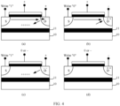
- the gate-all-around field-effect transistor further includes a plurality of insulation structures, where a first insulation structure in the plurality of insulation structures is disposed between the source region and the channel region, and a second insulation structure in the plurality of insulation structures is disposed between the channel region and the drain region.
- each insulation structure in the plurality of insulation structures spans the nanowire.
- references to "first”, “second” and similar terms herein do not imply any order, quantity or importance, but are merely intended to distinguish between different components. Similarly, similar words such as “a” or “an” do not imply a quantitative limit, but rather the existence of at least one.
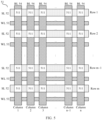
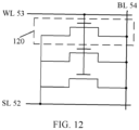
- the memory may be an embedded DRAM, or may be an SRAM, or the like.
- the memory and a logical device may be integrated in a same die, to implement high-speed data exchange between the memory and the logical device.
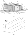
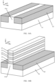
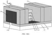
- a structure in which a semiconductor structure 21 (formed of the second semiconductor material) and a nanowire 63 (formed of the first semiconductor material) are sequentially stacked may be formed, as shown in FIG. 14B .
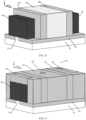
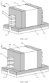
- the semiconductor material may be grown through an in-situ doping method, and then high-temperature annealing is performed on the semiconductor material to form the semiconductor structure 66.
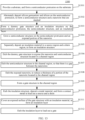
- S1305 Separately deposit an insulation material in a source region and a drain region, to form an insulation structure.
Landscapes
- Engineering & Computer Science (AREA)
- Manufacturing & Machinery (AREA)
- Semiconductor Memories (AREA)
- Thin Film Transistor (AREA)
Applications Claiming Priority (1)
| Application Number | Priority Date | Filing Date | Title |
|---|---|---|---|
| PCT/CN2021/071482 WO2022151044A1 (fr) | 2021-01-13 | 2021-01-13 | Mémoire, transistor à effet de champ à grille enveloppante et procédé de production |
Publications (2)
| Publication Number | Publication Date |
|---|---|
| EP4261889A1 true EP4261889A1 (fr) | 2023-10-18 |
| EP4261889A4 EP4261889A4 (fr) | 2024-03-13 |
Family
ID=82447685
Family Applications (1)
| Application Number | Title | Priority Date | Filing Date |
|---|---|---|---|
| EP21918260.7A Pending EP4261889A4 (fr) | 2021-01-13 | 2021-01-13 | Mémoire, transistor à effet de champ à grille enveloppante et procédé de production |
Country Status (4)
| Country | Link |
|---|---|
| US (1) | US20230352552A1 (fr) |
| EP (1) | EP4261889A4 (fr) |
| CN (1) | CN116601774A (fr) |
| WO (1) | WO2022151044A1 (fr) |
Cited By (1)
| Publication number | Priority date | Publication date | Assignee | Title |
|---|---|---|---|---|
| US20240431099A1 (en) * | 2023-06-21 | 2024-12-26 | Winbond Electronics Corp. | Semiconductor memory device and method for forming the same |
Family Cites Families (11)
| Publication number | Priority date | Publication date | Assignee | Title |
|---|---|---|---|---|
| KR101681396B1 (ko) * | 2011-12-19 | 2016-11-30 | 인텔 코포레이션 | 고전압 트랜지스터와 그 제조방법, 고전압 트랜지스터를 포함하는 시스템 온 칩 및 고전압 트랜지스터를 포함하는 이동 컴퓨팅 장치 |
| KR102037304B1 (ko) * | 2013-03-15 | 2019-10-29 | 인텔 코포레이션 | 하층 에칭 정지를 갖는 나노와이어 트랜지스터 |
| US9647139B2 (en) * | 2015-09-04 | 2017-05-09 | International Business Machines Corporation | Atomic layer deposition sealing integration for nanosheet complementary metal oxide semiconductor with replacement spacer |
| US10157992B2 (en) * | 2015-12-28 | 2018-12-18 | Qualcomm Incorporated | Nanowire device with reduced parasitics |
| US10643899B2 (en) * | 2018-07-27 | 2020-05-05 | International Business Machines Corporation | Gate stack optimization for wide and narrow nanosheet transistor devices |
| CN110875315B (zh) * | 2018-08-31 | 2025-02-07 | 长鑫存储技术有限公司 | 存储器及半导体器件 |
| US11101359B2 (en) * | 2018-11-28 | 2021-08-24 | Taiwan Semiconductor Manufacturing Company, Ltd. | Gate-all-around (GAA) method and devices |
| CN109599335A (zh) * | 2018-12-27 | 2019-04-09 | 中国科学院微电子研究所 | 环栅纳米线晶体管及其制备方法 |
| US10985161B2 (en) * | 2019-05-31 | 2021-04-20 | International Business Machines Corporation | Single diffusion break isolation for gate-all-around field-effect transistor devices |
| US11569370B2 (en) * | 2019-06-27 | 2023-01-31 | Intel Corporation | DEPOP using cyclic selective spacer etch |
| CN112151386B (zh) * | 2020-09-27 | 2023-01-06 | 中国科学院微电子研究所 | 堆叠纳米线环栅器件及其制作方法 |
-
2021
- 2021-01-13 WO PCT/CN2021/071482 patent/WO2022151044A1/fr not_active Ceased
- 2021-01-13 EP EP21918260.7A patent/EP4261889A4/fr active Pending
- 2021-01-13 CN CN202180080029.3A patent/CN116601774A/zh active Pending
-
2023
- 2023-07-11 US US18/350,348 patent/US20230352552A1/en active Pending
Cited By (1)
| Publication number | Priority date | Publication date | Assignee | Title |
|---|---|---|---|---|
| US20240431099A1 (en) * | 2023-06-21 | 2024-12-26 | Winbond Electronics Corp. | Semiconductor memory device and method for forming the same |
Also Published As
| Publication number | Publication date |
|---|---|
| US20230352552A1 (en) | 2023-11-02 |
| EP4261889A4 (fr) | 2024-03-13 |
| CN116601774A (zh) | 2023-08-15 |
| WO2022151044A1 (fr) | 2022-07-21 |
Similar Documents
| Publication | Publication Date | Title |
|---|---|---|
| US11309319B2 (en) | Structures and SRAM bit cells integrating complementary field-effect transistors | |
| US10418449B2 (en) | Circuits based on complementary field-effect transistors | |
| CN113540115A (zh) | 三维存储器件及其形成方法 | |
| CN104134668A (zh) | 存储器件及其制造方法和存取方法 | |
| US12513887B2 (en) | Semiconductor device and method for fabricating the same | |
| US12501602B2 (en) | 3D hybrid memory using horizontally oriented conductive dielectric channel regions | |
| TW202240851A (zh) | 製作半導體裝置的方法 | |
| US20240421216A1 (en) | Integrated circuit semiconductor device | |
| TW202137507A (zh) | 三維記憶體元件以及其製作方法 | |
| US20230352552A1 (en) | Memory, Gate-All-Around Field-Effect Transistor, and Manufacturing Method | |
| CN117279369A (zh) | 半导体器件及其制造方法 | |
| KR20230125597A (ko) | 반도체 장치 및 그 제조 방법 | |
| US12133387B2 (en) | 3D memory with conductive dielectric channel integrated with logic access transistors | |
| CN116896871A (zh) | 半导体器件及其制造方法 | |
| US20250081427A1 (en) | Semiconductor device and method for fabricating the same | |
| EP4658014A1 (fr) | Dispositif semi-conducteur et son procédé de fabrication | |
| US20250040117A1 (en) | Semiconductor device and method for fabricating the same | |
| TWI898772B (zh) | 包括具有較低和較高閘極電極層的字元線結構之記憶體元件及其製備方法 | |
| CN104112747B (zh) | 存储器件及其制造方法和存取方法 | |
| TWI919964B (zh) | 包括具有較低和較高閘極電極層的字元線結構之記憶體元件及其製備方法 | |
| US20240341080A1 (en) | Semiconductor device and method for fabricating the same | |
| US20260059780A1 (en) | Semiconductor device and method for fabricating the same | |
| US20250063717A1 (en) | Semiconductor device and method for fabricating the same | |
| CN119486124A (zh) | 半导体器件及用于制造半导体器件的方法 | |
| CN120021375A (zh) | 存储阵列及其制备方法、存储器、电子设备 |
Legal Events
| Date | Code | Title | Description |
|---|---|---|---|
| STAA | Information on the status of an ep patent application or granted ep patent |
Free format text: STATUS: THE INTERNATIONAL PUBLICATION HAS BEEN MADE |
|
| PUAI | Public reference made under article 153(3) epc to a published international application that has entered the european phase |
Free format text: ORIGINAL CODE: 0009012 |
|
| STAA | Information on the status of an ep patent application or granted ep patent |
Free format text: STATUS: REQUEST FOR EXAMINATION WAS MADE |
|
| 17P | Request for examination filed |
Effective date: 20230710 |
|
| AK | Designated contracting states |
Kind code of ref document: A1 Designated state(s): AL AT BE BG CH CY CZ DE DK EE ES FI FR GB GR HR HU IE IS IT LI LT LU LV MC MK MT NL NO PL PT RO RS SE SI SK SM TR |
|
| REG | Reference to a national code |
Ref country code: DE Ref legal event code: R079 Free format text: PREVIOUS MAIN CLASS: H01L0027108000 Ipc: H10B0012000000 |
|
| A4 | Supplementary search report drawn up and despatched |
Effective date: 20240213 |
|
| RIC1 | Information provided on ipc code assigned before grant |
Ipc: H01L 29/423 20060101ALI20240208BHEP Ipc: H01L 29/66 20060101ALI20240208BHEP Ipc: H01L 29/775 20060101ALI20240208BHEP Ipc: H01L 29/06 20060101ALI20240208BHEP Ipc: H10B 12/00 20230101AFI20240208BHEP |
|
| DAV | Request for validation of the european patent (deleted) | ||
| DAX | Request for extension of the european patent (deleted) |