EP4262073B1 - Elektrische leistungswandler - Google Patents
Elektrische leistungswandler Download PDFInfo
- Publication number
- EP4262073B1 EP4262073B1 EP22911593.6A EP22911593A EP4262073B1 EP 4262073 B1 EP4262073 B1 EP 4262073B1 EP 22911593 A EP22911593 A EP 22911593A EP 4262073 B1 EP4262073 B1 EP 4262073B1
- Authority
- EP
- European Patent Office
- Prior art keywords
- transistor
- resistor
- snubber
- circuit
- selection
- Prior art date
- Legal status (The legal status is an assumption and is not a legal conclusion. Google has not performed a legal analysis and makes no representation as to the accuracy of the status listed.)
- Active
Links
Images



Classifications
-
- H—ELECTRICITY
- H02—GENERATION; CONVERSION OR DISTRIBUTION OF ELECTRIC POWER
- H02M—APPARATUS FOR CONVERSION BETWEEN AC AND AC, BETWEEN AC AND DC, OR BETWEEN DC AND DC, AND FOR USE WITH MAINS OR SIMILAR POWER SUPPLY SYSTEMS; CONVERSION OF DC OR AC INPUT POWER INTO SURGE OUTPUT POWER; CONTROL OR REGULATION THEREOF
- H02M1/00—Details of apparatus for conversion
- H02M1/32—Means for protecting converters other than automatic disconnection
- H02M1/34—Snubber circuits
- H02M1/348—Passive dissipative snubbers
-
- H—ELECTRICITY
- H02—GENERATION; CONVERSION OR DISTRIBUTION OF ELECTRIC POWER
- H02M—APPARATUS FOR CONVERSION BETWEEN AC AND AC, BETWEEN AC AND DC, OR BETWEEN DC AND DC, AND FOR USE WITH MAINS OR SIMILAR POWER SUPPLY SYSTEMS; CONVERSION OF DC OR AC INPUT POWER INTO SURGE OUTPUT POWER; CONTROL OR REGULATION THEREOF
- H02M1/00—Details of apparatus for conversion
- H02M1/32—Means for protecting converters other than automatic disconnection
- H02M1/34—Snubber circuits
-
- H—ELECTRICITY
- H02—GENERATION; CONVERSION OR DISTRIBUTION OF ELECTRIC POWER
- H02M—APPARATUS FOR CONVERSION BETWEEN AC AND AC, BETWEEN AC AND DC, OR BETWEEN DC AND DC, AND FOR USE WITH MAINS OR SIMILAR POWER SUPPLY SYSTEMS; CONVERSION OF DC OR AC INPUT POWER INTO SURGE OUTPUT POWER; CONTROL OR REGULATION THEREOF
- H02M3/00—Conversion of DC power input into DC power output
- H02M3/02—Conversion of DC power input into DC power output without intermediate conversion into AC
- H02M3/04—Conversion of DC power input into DC power output without intermediate conversion into AC by static converters
- H02M3/10—Conversion of DC power input into DC power output without intermediate conversion into AC by static converters using discharge tubes with control electrode or semiconductor devices with control electrode
- H02M3/145—Conversion of DC power input into DC power output without intermediate conversion into AC by static converters using discharge tubes with control electrode or semiconductor devices with control electrode using devices of a triode or transistor type requiring continuous application of a control signal
- H02M3/155—Conversion of DC power input into DC power output without intermediate conversion into AC by static converters using discharge tubes with control electrode or semiconductor devices with control electrode using devices of a triode or transistor type requiring continuous application of a control signal using semiconductor devices only
-
- H—ELECTRICITY
- H02—GENERATION; CONVERSION OR DISTRIBUTION OF ELECTRIC POWER
- H02M—APPARATUS FOR CONVERSION BETWEEN AC AND AC, BETWEEN AC AND DC, OR BETWEEN DC AND DC, AND FOR USE WITH MAINS OR SIMILAR POWER SUPPLY SYSTEMS; CONVERSION OF DC OR AC INPUT POWER INTO SURGE OUTPUT POWER; CONTROL OR REGULATION THEREOF
- H02M3/00—Conversion of DC power input into DC power output
- H02M3/02—Conversion of DC power input into DC power output without intermediate conversion into AC
- H02M3/04—Conversion of DC power input into DC power output without intermediate conversion into AC by static converters
- H02M3/10—Conversion of DC power input into DC power output without intermediate conversion into AC by static converters using discharge tubes with control electrode or semiconductor devices with control electrode
- H02M3/145—Conversion of DC power input into DC power output without intermediate conversion into AC by static converters using discharge tubes with control electrode or semiconductor devices with control electrode using devices of a triode or transistor type requiring continuous application of a control signal
- H02M3/155—Conversion of DC power input into DC power output without intermediate conversion into AC by static converters using discharge tubes with control electrode or semiconductor devices with control electrode using devices of a triode or transistor type requiring continuous application of a control signal using semiconductor devices only
- H02M3/156—Conversion of DC power input into DC power output without intermediate conversion into AC by static converters using discharge tubes with control electrode or semiconductor devices with control electrode using devices of a triode or transistor type requiring continuous application of a control signal using semiconductor devices only with automatic control of output voltage or current, e.g. switching regulators
-
- Y—GENERAL TAGGING OF NEW TECHNOLOGICAL DEVELOPMENTS; GENERAL TAGGING OF CROSS-SECTIONAL TECHNOLOGIES SPANNING OVER SEVERAL SECTIONS OF THE IPC; TECHNICAL SUBJECTS COVERED BY FORMER USPC CROSS-REFERENCE ART COLLECTIONS [XRACs] AND DIGESTS
- Y02—TECHNOLOGIES OR APPLICATIONS FOR MITIGATION OR ADAPTATION AGAINST CLIMATE CHANGE
- Y02B—CLIMATE CHANGE MITIGATION TECHNOLOGIES RELATED TO BUILDINGS, e.g. HOUSING, HOUSE APPLIANCES OR RELATED END-USER APPLICATIONS
- Y02B70/00—Technologies for an efficient end-user side electric power management and consumption
- Y02B70/10—Technologies improving the efficiency by using switched-mode power supplies [SMPS], i.e. efficient power electronics conversion e.g. power factor correction or reduction of losses in power supplies or efficient standby modes
Definitions
- the present disclosure relates to a DC-DC (direct current-direct current) converter.
- the DC-DC converter converts an input voltage and supplies an output voltage having a required voltage level.
- a transient voltage may be generated according to voltage switching.
- a snubber circuit may be applied to the DC-DC converter to prevent component damage due to transient voltage and to remove EMI radiation noise.
- US 2020/0395842 A1 discloses a voltage regulator circuit designed to attenuate ringing in the switch node of a buck converter.
- the voltage regulator includes high-side and low-side field-effect transistors (FETs), an inductor, and a conductive net connecting these components.
- An attenuation circuit which includes an electronic switch, is coupled to the conductive net to control the amount of attenuation.
- the switchable snubber circuit is turned on by the controller to attenuate voltage spikes when needed, thereby reducing power dissipation during normal operation.
- the controller monitors the voltage or current and activates the snubber circuit when the measured values exceed set thresholds.
- US 2020/0204062 A1 discloses a snubber circuit, a control circuit, and an information processing apparatus aimed at reducing noise in circuits with switching elements, such as converters or inverters.
- the snubber circuit includes a first capacitor and a first resistor with a variable resistance value, which can be controlled by a control circuit.
- the information processing apparatus can measure radiation noise and adjust the resistance value of the snubber circuit based on the acquired noise information.
- the snubber circuit can also include multiple resistors and capacitors, with switching elements to vary their connections, further enhancing noise reduction capabilities.
- a DC-DC converter including a snubber circuit
- a DC-DC converter capable of variably applying a snubber value is provided.
- an electric power converter includes an integrated circuit including at least one power transistor and a snubber circuit connected in parallel to the at least one power transistor, and a selection resistor connected between a power supply voltage supplied to the integrated circuit and the snubber circuit, in which the snubber circuit includes at least two snubbers, and each of the at least two snubbers includes a resistor, a first transistor, and a capacitor connected in series, and the selection resistor is connected to a gate of the first transistor of any one of the at least two snubbers.
- the electric power converter further comprises a resistance box circuit.
- the resistance box circuit comprises, for each snubber, an individual resistance box connected to a gate of the first transistor of any the respective one of the at least two snubbers and to a power supply voltage (VCC) through selection terminals of the integrated circuit.
- At least one of the individual resistance boxes for the snubbers includes a selection resistor. Each selection resistor connects the gate of the transistor of the snubber corresponding to the respective individual resistance box to the power supply voltage (VCC) thereby turning on the transistor of said snubber corresponding to the respective individual resistance box.
- the first transistor of any one of the at least two snubbers may be turned on by the power supply voltage supplied through the selection resistor.
- the first transistor of the remaining snubber except any one of the at least two snubbers may be turned off.
- the integrated circuit may further include a switch control circuit configured to receive the power supply voltage and control a switching operation of the at least one power transistor.
- an electric power converter including: an integrated circuit including at least one power transistor and a snubber circuit connected in parallel to the at least one power transistor; and at least two selection resistors connected between a power supply voltage supplied to the integrated circuit and the snubber circuit, in which the snubber circuit includes at least two resistors, at least two first transistors connected in series to the at least two resistors, respectively, at least two capacitors, and at least two second transistors connected in series to the at least two capacitors, respectively.
- the electric power converter further comprises a resistance box circuit comprising a plurality of individual resistance boxes for the snubber circuit.
- Each of the individual resistance boxes is connected to either a gate of one of the first transistors and to a power supply voltage (VCC) through selection terminals of the integrated circuit, or to a gate of one of the second transistors and to the power supply voltage (VCC) through the selection terminals.
- At least two of the individual resistance boxes for the snubber circuit include a selection resistor. Each selection resistor connects either the gate of one of the first transistors or the gate of one of the second transistors to the power supply voltage (VCC) through the selection resistor of the respective individual resistance box to thereby turn on the respective first transistor or the respective second transistor.
- a first selection resistor of the at least two selection resistors is connected to the gate of one of the first transistors connected in series to any one of the at least two resistors, and a second selection resistor of the at least two selection resistors is connected to the gate of one of the second transistors connected in series to any one of the at least two capacitors.
- a first transistor connected in series to any one of the at least two resistors may be turned on by the power supply voltage supplied through the first selection resistor, and a second transistor connected in series to any one of the at least two capacitors may be turned on by the power supply voltage supplied through the second selection resistor.
- the first transistor connected in series to the remaining resistors except any one of the at least two resistors may be turned off, and the second transistor connected in series to the remaining capacitors except any one of the at least two capacitors may be turned off.
- the integrated circuit may further include a switch control circuit configured to receive the power supply voltage and control the at least one power transistor.
- the at least two selection resistors may include a third selection resistor that may be connected to a gate of a first transistor connected in series to another of the at least two resistors, and a resistance value of the snubber circuit may be a parallel synthesis resistance of one of the at least two resistors and another resistor.
- the at least two selection resistors may include a third selection resistor that may be connected to a gate of a second transistor connected in series to another of the at least two capacitors, and a capacitance value of the snubber circuit may be a parallel synthesis capacitance of one of the at least two capacitors and another capacitor.
- the electric power converter may be a DC-DC converter.
- a DC-DC converter including a snubber circuit
- a DC-DC converter capable of selectively configuring a snubber circuit among a plurality of snubbers or variably applying a resistance value and a capacitance of the snubber circuit may be provided.
- FIGS. 1 to 7 illustrate a converter circuit for converting an input DC voltage into a DC voltage, which allows a snubber circuit to be variously configured.
- FIG. 1 is a block diagram schematically illustrating a converter according to an exemplary embodiment.
- the converter 1 may DC-DC-convert an input voltage Vin and output an output voltage Vout.
- the converter 1 includes an integrated circuit (IC) 10, a resistance box 20, and an output unit 30.
- the converter 1 may be mounted on a printed circuit board (PCB).
- the power supply voltage VCC may be supplied to the IC 10 through the terminal P1, and the power supply voltage VCC is supplied to the resistance box 20.
- the input voltage Vin may be supplied to the IC 10 through the terminal P2.
- the IC 10 may DC-DC-convert an input voltage Vin and transmit an output voltage to the output unit 30 through a terminal P4 and a terminal P5.
- the input voltage Vin may be connected to the terminals P2 and P3
- the resistance box 20 selects a configuration of the IC 10 through the plurality of selection terminals P11 to P13.
- FIG. 1 illustrates that the IC 10 includes three selection terminals P11 to P13, the disclosure is not limited thereto, and the IC 10 may be implemented to include two or more selection terminals.
- the IC 10 may convert an input voltage through a plurality of transistors and a switch control circuit.
- the IC 10 may include a switch control circuit 110, a first power transistor Q1, a first resistor R1, a first capacitor C1, a second power transistor Q2, a snubber circuit 120, and an inductor L.
- the switch control circuit 110 may generate transistor control signals QCS1 and QCS2 for controlling switching operations of the first and second power transistors Q1 and Q2 by using the power supply voltage VCC input through the terminal P1 as a power source. Switching operations of the first power transistor Q1 and the second power transistor Q2 may be controlled according to transistor control signals QCS1 and QCS2 supplied from the switch control circuit 110.
- the first resistor R1 and the first capacitor C1 are connected to each other in series, and are connected to the first power transistor Q1 in parallel.
- One end of the first power transistor Q1 is connected to one end of the switch control circuit 110.
- the other end of the first power transistor Q1 is connected to a node to which one end of the second power transistor Q2, a terminal P21 of the snubber circuit 120, and one end of the inductor L are connected.
- the other end of the second power transistor Q2 is connected to a node to which the other end of the switch control circuit 110 and the terminal P22 of the snubber circuit 120 are connected.
- Terminal P23 of snubber circuit 120 is connected to terminal P5 of IC 10.
- the other end of the inductor L is connected to a terminal P4, and a terminal P23 of the snubber circuit 120 is connected to a terminal P5.
- the output unit 30 may include a capacitor C and a load R.
- one end of the output voltage Vout is connected to a node to which one end of the capacitor C and one end of the load R are connected, and the other end of the output voltage Vout is connected to a node to which the other end of the capacitor C and the other end of the load R are connected.
- the on-level of the transistor control signals QCS1 and QCS2 is a high level, and the off-level thereof is a low level.
- the input voltage Vin is supplied to the inductor L so that the current flowing through the inductor L may increase.
- the first power transistor Q1 is turned off and the second power transistor Q2 is turned on by the transistor control signal QCS1 of the low level and the transistor control signal QCS2 of the high level, the current flowing through the inductor L may decrease while flowing through the second power transistor Q2.
- a current flowing through the inductor L may be supplied to the load R, and the output voltage Vout may be smoothed to a constant level by the capacitor C.
- the switch control circuit 110 may sense the output voltage Vout and may control switching operations of the first and second power transistors Q1 and Q2 so that the output voltage Vout may be maintained at a predetermined level.
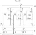
- FIG. 2 is a circuit diagram illustrating an example of implementing a snubber circuit and a resistance box according to a first embodiment of the invention.
- the snubber circuit according to an example illustrated in FIG. 2 is configured to operate in a snubber unit in which a resistor, a capacitor, and a transistor are connected in series.
- the snubber circuit 120 includes a first snubber 121, a second snubber 122, a third snubber 123, and a plurality of gate resistors RG21 to RG23.
- the first snubber 121 includes a resistor R21, a capacitor C21, and a transistor Q21
- the second snubber 122 includes a resistor R22, a capacitor C22, and a transistor Q22
- the third snubber 123 includes a resistor R23, a capacitor C23, and a transistor Q23.
- FIG. 2 illustrates that the snubber circuit 120 includes three snubbers 121 to 123, the present disclosure is not limited thereto, and the snubber circuit 120 may be implemented as including two or more snubbers. As illustrated in FIG. 2 , the number of selection terminals P11 to P13 may be increased or decreased based on the number of snubbers included in the snubber circuit 120.
- One end of the first snubber 121, one end of the second snubber 122, and one end of the third snubber 123 are connected to a terminal P21, and the other end of the first snubber 121, the other end of the second snubber 122, and the other end of the third snubber 123 are connected to a node to which the terminal P22 and the terminal P23 are connected.
- the terminal P21 is connected to a node to which one end of the resistor R21, one end of the resistor R22, and one end of the resistor R23 are connected.
- the other end of the resistor R21 is connected to one end of the transistor Q21.
- the other end of the transistor Q21 is connected to one end of the capacitor C21.
- One end of the gate resistor RG21 is connected to the gate end of the transistor Q21, and the other end of the gate resistor RG21 is connected to the selection terminal P11.
- the other end of the resistor R22 is connected to one end of the transistor Q22.
- the other end of the transistor Q22 is connected to one end of the capacitor C22.
- One end of the gate resistor RG22 is connected to the gate end of the transistor Q22, and the other end of the gate resistor RG22 is connected to the selection terminal P12.
- the other end of the resistor R23 is connected to one end of the transistor Q23.
- the other end of the transistor Q23 is connected to one end of the capacitor C23.
- One end of the gate resistor RG23 is connected to the gate end of the transistor Q23, and the other end of the gate resistor RG23 is connected to the selection terminal P13.
- the other end of the capacitor C21, the other end of the capacitor C22, and the other end of the capacitor C23 are connected to the node to which the terminal P22 and the terminal P23 are connected.
- the snubber circuit 120 operates through at least one selected from among the first snubber 121, the second snubber 122, and the third snubber 123 according to the configuration of the resistance box 20.
- the resistance box 20 includes a plurality of individual resistance boxes 21 to 23.
- the resistance box 20 is illustrated as including three individual resistance boxes 21 to 23, but the present disclosure is not limited thereto, and the resistance box 20 may be implemented as including two or more individual resistance boxes.
- the number of individual resistance boxes may be increased or decreased based on the number of selection terminals P11 to P13.
- Each of a plurality of individual resistance boxes 21 to 23 may include a selection resistor.
- each of a plurality of individual resistance boxes 21 to 23 may be an open circuit.
- a resistance box that does not include the selection resistor among the plurality of individual resistance boxes 21 to 23 will be described as being open.
- FIG. 3 is a circuit diagram illustrating an example of a resistance box according to an exemplary embodiment.
- the selection resistor RS1 is included in the individual resistance box 21, and the selection resistor is not included in the remaining individual resistance boxes 22 and 23.
- the power supply voltage VCC supplied to the resistance box 20 may supply a current to a corresponding selection terminal (e.g., P11) among the plurality of selection terminals P11 to P13 through an individual resistance box (e.g., 21) including a selection resistor among the plurality of individual resistance boxes 21 to 23.
- a corresponding selection terminal e.g., P11
- an individual resistance box e.g., 21
- selection resistor among the plurality of individual resistance boxes 21 to 23.
- the transistor Q21 is turned on by the power supply voltage VCC supplied through the resistor RS1 and the resistor RG21.
- the first snubber 121 is connected in parallel to the second power transistor Q2. That is, the first snubber 121 may operate with respect to a transient voltage that may occur during a switching operation of the second power transistor Q2.
- the resistance value of the snubber circuit 120 may be the resistance value of the resistor R21, and the capacitance of the snubber circuit 120 may be determined as the capacitance of the capacitor C21.
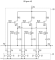
- FIG. 4 is a circuit diagram illustrating an example of implementing a snubber circuit and a resistance box according to a second embodiment of the invention.
- the snubber circuit according to an exemplary embodiment illustrated in FIG. 4 may not operate in a snubber unit, unlike the snubber circuit according to an exemplary embodiment illustrated in FIG. 2 .
- the snubber circuit 120 includes a plurality of resistors R21 to R23, a plurality of capacitors C21 to C23, a plurality of transistors Q21 to Q23, Q211, Q221, and Q231, and a plurality of gate resistors RG21 to RG23, RG211, RG221, and RG231.
- the terminal P21 is connected to a node to which one end of the resistor R21, one end of the resistor R22, and one end of the resistor R23 are connected.
- the other end of the resistor R21 is connected to one end of the transistor Q21.
- One end of the gate resistor RG21 is connected to the gate end of the transistor Q21, and the other end of the gate resistor RG21 is connected to the selection terminal P11.
- One end of the transistor Q211 is connected to one end of the capacitor C21.
- One end of the gate resistor RG211 is connected to the gate end of the transistor Q211, and the other end of the gate resistor RG211 is connected to the selection terminal P14.
- the other end of the resistor R22 is connected to one end of the transistor Q22.
- One end of the gate resistor RG22 is connected to the gate end of the transistor Q22, and the other end of the gate resistor RG22 is connected to the selection terminal P12.
- One end of the transistor Q221 is connected to one end of the capacitor C22.
- One end of the gate resistor RG221 is connected to the gate end of the transistor Q221, and the other end of the gate resistor RG221 is connected to the selection terminal P15.
- the other end of the resistor R23 is connected to one end of the transistor Q23.
- One end of the gate resistor RG23 is connected to the gate end of the transistor Q23, and the other end of the gate resistor RG23 is connected to the selection terminal P13.
- One end of the transistor Q231 is connected to one end of the capacitor C23.
- One end of the gate resistor RG231 is connected to the gate end of the transistor Q231, and the other end of the gate resistor RG231 is connected to the selection terminal P16.
- the other end of the transistor Q21, the other end of the transistor Q211, the other end of the transistor Q22, the other end of the transistor Q221, the other end of the transistor Q23, and the other end of the transistor Q231 are connected to the node NN.
- the other end of the capacitor C21, the other end of the capacitor C22, and the other end of the capacitor C23 are connected to the node to which the terminal P22 and the terminal P23 are connected.
- the snubber circuit 120 operates through at least one selected according to the configuration of the resistance box 20 among the plurality of resistors R21 to R23 and at least one selected according to the configuration of the resistance box 20 among the plurality of capacitors C21 to C23.
- the resistance box 20 includes a plurality of individual resistance boxes 21 to 26.
- the resistance box 20 is illustrated as including six individual resistance boxes 21 to 26, and the number of selection terminals P11 to P16 is illustrated as six.
- Each of a plurality of individual resistance boxes 21 to 26 may include a selection resistor.
- each of a plurality of individual resistance boxes 21 to 26 may be an open circuit.
- a resistance box that does not include the selection resistor among the plurality of individual resistance boxes 21 to 26 will be described as being open.
- FIG. 5 is a circuit diagram illustrating an example of a resistance box according to an exemplary embodiment.
- the individual resistance box 21 includes the selection resistor RS1
- the individual resistance box 25 includes the selection resistor RS5
- the remaining individual resistance boxes 22 to 24 and 26 do not include the selection resistor.
- the power supply voltage VCC supplied to the resistance box 20 may supply a current to a corresponding one of the plurality of selection terminals P11 to P16 (e.g., P11 and P15) through an individual resistance box (e.g., 21 and 25) including a selection resistor among the plurality of individual resistance boxes 21 to 26.
- the transistor Q21 is turned on by the power supply voltage VCC supplied through the resistor RS1 and the resistor RG21, and the transistor Q221 is turned on by the power supply voltage VCC supplied through the resistor RS5 and the resistor RG221.
- the resistor R21 and the capacitor C22 are connected in parallel to the second power transistor Q2 by the transistor Q21 and the transistor Q221 being turned on.
- the resistance value of the snubber circuit 120 may be the resistance value of the resistor R21, and the capacitance of the snubber circuit 120 may be determined as the capacitance of the capacitor C22.
- the resistance value of the snubber circuit 120 may be determined as a composite resistance using a plurality of resistors, or the capacitance of the snubber circuit 120 may be determined as a composite capacitance using a plurality of capacitors.
- FIG. 6 is a circuit diagram illustrating an example of a resistance box according to an exemplary embodiment.
- the individual resistance box 21 includes the selection resistor RS1
- the individual resistance box 23 includes the selection resistor RS3
- the individual resistance box 25 includes the selection resistor RS5
- the remaining individual resistance boxes 22, 24, and 26 do not include the selection resistor.
- the power supply voltage VCC supplied to the resistance box 20 may supply a current to a corresponding selection terminal (e.g., P11, P13, and P15) among the plurality of selection terminals P11 to P16 through an individual resistance box (e.g., 21, 23, and 25) including a selection resistor among the plurality of individual resistance boxes 21 to 26.
- a corresponding selection terminal e.g., P11, P13, and P15
- an individual resistance box e.g., 21, 23, and 25
- a selection resistor among the plurality of individual resistance boxes 21 to 26.
- the transistor Q21 is turned on by the power supply voltage VCC supplied through the resistor RS1 and the resistor RG21
- the transistor Q23 is turned on by the power supply voltage VCC supplied through the resistor RS3 and the resistor RG23
- the transistor Q221 is turned on by the power supply voltage VCC supplied through the resistor RS5 and the resistor RG221.
- the resistance value of the snubber circuit 120 may be a parallel synthesis resistance value of the resistor R21 and the resistor R23, and the capacitance of the snubber circuit 120 may be determined as the capacitance of the capacitor C22.
- FIG. 7 is a circuit diagram illustrating an example of a resistance box according to an exemplary embodiment.
- the selection resistor RS1 is included in the individual resistance box 21
- the selection resistor RS5 is included in the individual resistance box 25
- the selection resistor RS6 is included in the individual resistance box 26
- the selection resistor is not included in the remaining individual resistance boxes 22 to 24.
- the power supply voltage VCC supplied to the resistance box 20 may supply a current to a corresponding selection terminal (e.g., P11, P15, and P16) among the plurality of selection terminals P11 to P16 through an individual resistance box (e.g., 21, 25, and 26) including a selection resistor among the plurality of individual resistance boxes 21 to 26.
- a corresponding selection terminal e.g., P11, P15, and P16
- an individual resistance box e.g., 21, 25, and 26
- a selection resistor among the plurality of individual resistance boxes 21 to 26.
- the transistor Q21 is turned on by the power supply voltage VCC supplied through the resistor RS1 and the resistor RG21
- the transistor Q221 is turned on by the power supply voltage VCC supplied through the resistor RS5 and the resistor RG22
- the transistor Q231 is turned on by the power supply voltage VCC supplied through the resistor RS6 and the resistor RG231.
- the transistor Q21, the transistor Q221, and the transistor Q231 are turned on, the resistor R21, the capacitor C22, and the capacitor C23 are connected in parallel to the second power transistor Q2.
- the resistance value of the snubber circuit 120 may be the resistance value of the resistor R21, and the capacitance of the snubber circuit 120 may be determined as the parallel synthesis capacitance of the capacitor C22 and the capacitor C23.
- the snubber circuit 120 may include a plurality of resistors as illustrated in FIGS. 4 and 6 , or may include a plurality of capacitors as illustrated in FIGS. 4 and 7 .
- the snubber circuit 120 may include a resistance box in which the resistance box illustrated in FIG. 6 and the resistance box illustrated in FIG. 7 are combined to include a plurality of resistors and a plurality of capacitors.
- noise that may be generated in the second power transistor Q2 may be reduced, and a snubber value of the snubber circuit 120 installed in the IC 10 may be adjusted according to a configuration of a selection resistor included in the resistance box 20 located outside the IC 10.
- the snubber value may be adjusted outside the IC 10 to reduce the debugging time for noise removal.
Landscapes
- Engineering & Computer Science (AREA)
- Power Engineering (AREA)
- Power Conversion In General (AREA)
- Dc-Dc Converters (AREA)
- Direct Current Feeding And Distribution (AREA)
Claims (10)
- Elektrischer Leistungswandler, aufweisend:eine integrierte Schaltung (10) mit mindestens einem Leistungstransistor (Q1, Q2) und einer Snubber-Schaltung (120), die parallel zu dem mindestens einen Leistungstransistor (Q1, Q2) geschaltet ist; unddadurch gekennzeichnet, dassdie Snubber-Schaltung (120) mindestens zwei Snubber (121, 122, 123) aufweist, undjeder der mindestens zwei Snubber (121, 122, 123) einen Widerstand (R21, R22, R23), einen Transistor (Q21, Q22, Q23) und einen Kondensator (C21, C22, C23) aufweist, die in Reihe geschaltet sind, undder elektrische Leistungswandler ferner eine Widerstandskastenschaltung (20) aufweist, die für jeden Snubber (121, 122, 123) einen individuellen Widerstandskasten (21, 22, 23) aufweist, der mit einem Gate des Transistors (Q21, Q22, Q23) des jeweiligen der mindestens zwei Snubber (121, 122, 123) durch einen entsprechenden Auswahlanschluss (P11, P12, P13) der integrierten Schaltung (10) verbunden ist und mit einer Leistungsversorgungsspannung (VCC) verbindbar ist,wobei mindestens einer der individuellen Widerstandskästen (21) für die Snubber (121) einen Auswahlwiderstand aufweist, wobei jeder Auswahlwiderstand konfiguriert ist, das Gate des Transistors (Q21, Q22, Q23) des Snubber (121), der dem jeweiligen individuellen Widerstandskasten (21) entspricht, mit der Leistungsversorgungsspannung (VCC) zu verbinden, um den Transistor (Q21) des Snubber (121), der dem jeweiligen individuellen Widerstandskasten (21) entspricht, einzuschalten.
- Elektrischer Leistungswandler nach Anspruch 1, wobei mindestens einer der individuellen Widerstandskästen (22, 23) für die Snubber (122, 123) keinen Auswahlwiderstand aufweist, wobei jeder individuelle Widerstandskasten (22, 23), der keinen Auswahlwiderstand aufweist, einen offenen Stromkreis zwischen dem Gate des Transistors (Q22, Q23) des Snubber (122, 123), der dem jeweiligen individuellen Widerstandskasten (22, 23) entspricht, und der Leistungsversorgungsspannung (VCC) bereitstellt, wodurch der Snubber (122, 123), der dem jeweiligen individuellen Widerstandskasten (22, 23) entspricht, ausgeschaltet wird.
- Elektrischer Leistungswandler nach Anspruch 1 oder 2, wobei:
die integrierte Schaltung (10) ferner eine Schaltsteuerschaltung (110) aufweist, die konfiguriert ist, die Leistungsversorgungsspannung (VCC) zu empfangen und einen Schaltvorgang des mindestens einen Leistungstransistors (Q1, Q2) zu steuern. - Elektrischer Leistungswandler nach einem der Ansprüche 1 bis 3, wobei der elektrische Leistungswandler ein DC-DC-Wandler ist.
- Elektrischer Leistungswandler, aufweisend:eine integrierte Schaltung (10) mit mindestens einer Snubber-Schaltung (120), die parallel zu dem mindestens einen Leistungstransistor (Q1, Q2) geschaltet ist; unddie Snubber-Schaltung (120) aufweist:mindestens zwei Widerstände (R21, R22, R23),mindestens zwei erste Transistoren (Q21, Q22, Q23),mindestens zwei Kondensatoren (C21, C22, C23), undmindestens zwei zweite Transistoren (Q211, Q221, Q231), die jeweils in Reihe mit jedem der mindestens zwei Kondensatoren (C21, C22, C23) geschaltet sind, unddadurch gekennzeichnet, dassdie integrierte Schaltung (10) ferner einen Leistungstransistor (Q1, Q2) aufweist;die mindestens zwei ersten Transistoren (Q21, Q22, Q23) jeweils in Reihe mit den mindestens zwei Widerständen (R21, R22, R23) geschaltet sind, undwobei der elektrische Leistungswandler ferner eine Widerstandskastenschaltung (20) aufweist, die mehrere individuelle Widerstandskästen (21-26) für die Snubber-Schaltung (120) aufweist, wobei jeder individuelle Widerstandskasten eines ersten Satzes der individuellen Widerstandskästen (21, 22, 23) mit einem Gate eines der ersten Transistoren (Q21, Q22, Q23) durch einen entsprechenden Auswahlanschluss (P11, P12, P13) der integrierten Schaltung (10) verbunden ist und mit einer Leistungsversorgungsspannung (VCC) verbindbar ist, und jeder individuelle Widerstandskasten eines zweiten Satzes von Widerstandskästen (24, 25, 26) mit einem Gate eines der zweiten Transistoren (Q211, Q221, Q231) durch einen entsprechenden Auswahlanschluss (P14, P15, P16) der integrierten Schaltung (10) verbunden ist und mit der Leistungsversorgungsspannung (VCC) verbindbar ist,wobei mindestens zwei der individuellen Widerstandskästen (21, 25) für die Snubber-Schaltung (120) einen Auswahlwiderstand aufweisen, wobei jeder Auswahlwiderstand konfiguriert ist, entweder das Gate eines der ersten Transistoren (Q21) oder das Gate eines der zweiten Transistoren (Q221) mit der Leistungsversorgungsspannung (VCC) durch den Auswahlwiderstand des jeweiligen individuellen Widerstandskastens (21, 25) zu verbinden, um dadurch den jeweiligen ersten Transistor (Q21) oder den jeweiligen zweiten Transistor (Q221) einzuschalten, undwobei ein erster Auswahlwiderstand der mindestens zwei Auswahlwiderstände (RS1) mit dem Gate eines der ersten Transistoren (Q21) verbunden ist, der in Reihe mit einem der mindestens zwei Widerstände (R21) geschaltet ist, und ein zweiter Auswahlwiderstand der mindestens zwei Auswahlwiderstände (RS5) mit dem Gate eines der zweiten Transistoren (Q221) verbunden ist, der in Reihe mit einem der mindestens zwei Kondensatoren (C22) geschaltet ist.
- Elektrischer Leistungswandler nach Anspruch 5, wobei:
wobei mindestens einer der individuellen Widerstandskästen (22, 24) für die Snubber-Schaltung (120) keinen Auswahlwiderstand aufweist, wobei jeder individuelle Widerstandskasten (22, 24), der keinen Auswahlwiderstand aufweist, einen offenen Stromkreis zwischen dem Gate des ersten Transistors (Q22), der dem jeweiligen individuellen Widerstandskasten (22) entspricht, und der Leistungsversorgungsspannung (VCC) oder zwischen dem Gate des zweiten Transistors (Q211), der dem jeweiligen individuellen Widerstandskasten (24) entspricht, und der Leistungsversorgungsspannung (VCC) bereitstellt, wodurch der jeweilige erste Transistor (Q22) oder der jeweilige zweite Transistor (Q211), der dem jeweiligen individuellen Widerstandskasten (22, 24) entspricht, ausgeschaltet wird. - Elektrischer Leistungswandler nach Anspruch 5 oder 6, wobei:
die integrierte Schaltung (10) ferner eine Schaltsteuerschaltung (110) aufweist, die konfiguriert ist, die Leistungsversorgungsspannung (VCC) zu empfangen, um den mindestens einen Leistungstransistor (Q1, Q2) zu steuern. - Elektrischer Leistungswandler nach einem der Ansprüche 5 bis 7, wobei:
ein Widerstandswert der Snubber-Schaltung (120) ein paralleler Synthesewiderstand von mindestens zwei der mindestens zwei Widerstände (R21, R22, R23) ist. - Elektrischer Leistungswandler nach einem der Ansprüche 5 bis 8, wobei:die mindestens zwei Auswahlwiderstände ferner einen dritten Auswahlwiderstand aufweisen, der mit einem Gate eines der zweiten Transistoren (Q231) verbunden ist, der in Reihe mit einem anderen der mindestens zwei Kondensatoren (C23) geschaltet ist, undein Kapazitätswert der Snubber-Schaltung (120) eine parallele Synthesekapazität eines der mindestens zwei Kondensatoren (C22) und eines anderen (C23) ist.
- Elektrischer Leistungswandler nach einem der Ansprüche 5 bis 9, wobei der elektrische Leistungswandler ein DC-DC-Wandler ist.
Applications Claiming Priority (2)
| Application Number | Priority Date | Filing Date | Title |
|---|---|---|---|
| KR1020210182457A KR102954859B1 (ko) | 2021-12-20 | 2021-12-20 | Dc-dc 컨버터 |
| PCT/KR2022/016944 WO2023120955A1 (ko) | 2021-12-20 | 2022-11-01 | Dc-dc 컨버터 |
Publications (3)
| Publication Number | Publication Date |
|---|---|
| EP4262073A1 EP4262073A1 (de) | 2023-10-18 |
| EP4262073A4 EP4262073A4 (de) | 2024-07-24 |
| EP4262073B1 true EP4262073B1 (de) | 2025-05-28 |
Family
ID=86902882
Family Applications (1)
| Application Number | Title | Priority Date | Filing Date |
|---|---|---|---|
| EP22911593.6A Active EP4262073B1 (de) | 2021-12-20 | 2022-11-01 | Elektrische leistungswandler |
Country Status (9)
| Country | Link |
|---|---|
| US (1) | US12362657B2 (de) |
| EP (1) | EP4262073B1 (de) |
| JP (1) | JP7679585B2 (de) |
| KR (1) | KR102954859B1 (de) |
| CN (1) | CN116830443A (de) |
| ES (1) | ES3039693T3 (de) |
| HU (1) | HUE071876T2 (de) |
| PL (1) | PL4262073T3 (de) |
| WO (1) | WO2023120955A1 (de) |
Family Cites Families (18)
| Publication number | Priority date | Publication date | Assignee | Title |
|---|---|---|---|---|
| JPH05276654A (ja) | 1992-03-21 | 1993-10-22 | Ngk Insulators Ltd | 半導体素子の保護方法 |
| JPH08250310A (ja) | 1995-03-09 | 1996-09-27 | Yokogawa Electric Corp | 抵抗のトリミング回路 |
| KR101239801B1 (ko) | 2006-07-18 | 2013-03-06 | 엘지전자 주식회사 | 에스엠피에스 피드백 전원 장치 |
| JP5138002B2 (ja) | 2010-06-17 | 2013-02-06 | Tdkラムダ株式会社 | Dcdcコンバータ |
| JP5742227B2 (ja) | 2011-01-06 | 2015-07-01 | 株式会社デンソー | スイッチング装置 |
| JP5456096B2 (ja) | 2012-05-23 | 2014-03-26 | 三菱電機株式会社 | 誘導加熱調理器 |
| CN107667461A (zh) | 2015-05-27 | 2018-02-06 | 皇家飞利浦有限公司 | Dc到dc转换器 |
| WO2017082885A1 (en) | 2015-11-10 | 2017-05-18 | General Electric Company | Active snubber system and method of operating the same |
| JP6910115B2 (ja) | 2016-07-28 | 2021-07-28 | Fdk株式会社 | アクティブスナバ回路 |
| US9768678B1 (en) | 2016-11-16 | 2017-09-19 | Silanna Asia Pte Ltd | Switching regulator synchronous node snubber circuit |
| CN106953511B (zh) * | 2017-04-28 | 2019-06-21 | 昆山龙腾光电有限公司 | 开关电源电路及其调节方法 |
| JP7053291B2 (ja) | 2018-02-05 | 2022-04-12 | Fdk株式会社 | 電力変換装置 |
| KR102140951B1 (ko) | 2018-11-12 | 2020-08-05 | 엘지전자 주식회사 | 전력 공급 장치 및 이를 포함하는 공기조화기 |
| JP2020103008A (ja) | 2018-12-25 | 2020-07-02 | 日本電産株式会社 | スナバ回路、制御回路、及び情報処理装置 |
| KR102707050B1 (ko) * | 2019-02-15 | 2024-09-13 | 삼성전자주식회사 | 고조파들을 억압하는 전압 변환기 |
| US10910940B2 (en) * | 2019-06-13 | 2021-02-02 | Lenovo Enterprise Solutions (Singapore) Pte. Ltd. | Voltage regulator having a switchable attenuation circuit |
| JP7327016B2 (ja) | 2019-09-05 | 2023-08-16 | 株式会社村田製作所 | スナバ回路、及び、電力変換回路 |
| US12424930B2 (en) * | 2023-01-09 | 2025-09-23 | Texas Instruments Incorporated | Active snubber circuit |
-
2021
- 2021-12-20 KR KR1020210182457A patent/KR102954859B1/ko active Active
-
2022
- 2022-11-01 JP JP2023537088A patent/JP7679585B2/ja active Active
- 2022-11-01 HU HUE22911593A patent/HUE071876T2/hu unknown
- 2022-11-01 ES ES22911593T patent/ES3039693T3/es active Active
- 2022-11-01 EP EP22911593.6A patent/EP4262073B1/de active Active
- 2022-11-01 PL PL22911593.6T patent/PL4262073T3/pl unknown
- 2022-11-01 CN CN202280014429.9A patent/CN116830443A/zh active Pending
- 2022-11-01 WO PCT/KR2022/016944 patent/WO2023120955A1/ko not_active Ceased
- 2022-11-01 US US18/274,428 patent/US12362657B2/en active Active
Also Published As
| Publication number | Publication date |
|---|---|
| PL4262073T3 (pl) | 2025-10-06 |
| JP7679585B2 (ja) | 2025-05-20 |
| HUE071876T2 (hu) | 2025-09-28 |
| CN116830443A (zh) | 2023-09-29 |
| JP2024503580A (ja) | 2024-01-26 |
| KR20230093646A (ko) | 2023-06-27 |
| KR102954859B1 (ko) | 2026-04-17 |
| US20240106324A1 (en) | 2024-03-28 |
| EP4262073A1 (de) | 2023-10-18 |
| US12362657B2 (en) | 2025-07-15 |
| ES3039693T3 (en) | 2025-10-23 |
| WO2023120955A1 (ko) | 2023-06-29 |
| EP4262073A4 (de) | 2024-07-24 |
Similar Documents
| Publication | Publication Date | Title |
|---|---|---|
| USRE37738E1 (en) | Simple and efficient switching regulator for fast transient loads such as microprocessors | |
| KR102369236B1 (ko) | 단일 제어 루프를 갖는 다중-출력 부스트 레귤레이터 | |
| CN101931321B (zh) | 电源转换电路 | |
| US10177650B2 (en) | Switching regulator synchronous node snubber circuit | |
| US10432093B2 (en) | Multiphase DC-DC converter with configurable current sharing and phase management | |
| US7380146B2 (en) | Power management system | |
| US20170237349A1 (en) | Multi-master power controller with multiple feedback loops | |
| CN102239628A (zh) | 用于减少来自环振荡的emi的切换功率转换器及其控制方法 | |
| US8076918B2 (en) | Multi-phase driving circuit with phase adjusting function | |
| EP2485379B1 (de) | Stromversorgungsschaltung mit skalierbarer leistung und verfahren zum betrieb einer stromversorgungsschaltung | |
| EP4262073A1 (de) | Gleichspannungswandler | |
| EP1979798A2 (de) | Schaltung und verfahren zum ändern der flüchtigen reaktionsmerkmale eines gleichstrom-/wechselstromwandlermoduls | |
| EP1780880A2 (de) | Leistungswandler mit auf getrennte Leiterplatte angebrachten Steuervorrichtung und Leistungsbestandteil | |
| JP6071205B2 (ja) | Dc/dcコンバータ | |
| US20230318442A1 (en) | Battery surge reduction based on early warning signal | |
| US6661117B2 (en) | Load driving system and method thereof | |
| JP3732734B2 (ja) | 昇圧チョッパ回路 | |
| WO2009123644A1 (en) | Dc-to-dc converter with independent compensation logic | |
| US20260031717A1 (en) | Multi-phase power converter circuit layout to minimize drive loop and power loop inductances | |
| US20250233514A1 (en) | Power conversion device | |
| US10673329B2 (en) | Multiphase voltage regulator | |
| EP4736305A1 (de) | Pulsfrequenzmodulationsmodus für einen mehrphasigen wandler | |
| JP2024119597A (ja) | マルチフェーズdc/dcコンバータならびにそのコントローラ回路 |
Legal Events
| Date | Code | Title | Description |
|---|---|---|---|
| STAA | Information on the status of an ep patent application or granted ep patent |
Free format text: STATUS: THE INTERNATIONAL PUBLICATION HAS BEEN MADE |
|
| PUAI | Public reference made under article 153(3) epc to a published international application that has entered the european phase |
Free format text: ORIGINAL CODE: 0009012 |
|
| STAA | Information on the status of an ep patent application or granted ep patent |
Free format text: STATUS: REQUEST FOR EXAMINATION WAS MADE |
|
| 17P | Request for examination filed |
Effective date: 20230712 |
|
| AK | Designated contracting states |
Kind code of ref document: A1 Designated state(s): AL AT BE BG CH CY CZ DE DK EE ES FI FR GB GR HR HU IE IS IT LI LT LU LV MC ME MK MT NL NO PL PT RO RS SE SI SK SM TR |
|
| A4 | Supplementary search report drawn up and despatched |
Effective date: 20240625 |
|
| RIC1 | Information provided on ipc code assigned before grant |
Ipc: H02M 3/155 20060101ALI20240619BHEP Ipc: H02M 1/34 20070101AFI20240619BHEP |
|
| GRAP | Despatch of communication of intention to grant a patent |
Free format text: ORIGINAL CODE: EPIDOSNIGR1 |
|
| STAA | Information on the status of an ep patent application or granted ep patent |
Free format text: STATUS: GRANT OF PATENT IS INTENDED |
|
| DAV | Request for validation of the european patent (deleted) | ||
| DAX | Request for extension of the european patent (deleted) | ||
| INTG | Intention to grant announced |
Effective date: 20250306 |
|
| GRAS | Grant fee paid |
Free format text: ORIGINAL CODE: EPIDOSNIGR3 |
|
| GRAA | (expected) grant |
Free format text: ORIGINAL CODE: 0009210 |
|
| STAA | Information on the status of an ep patent application or granted ep patent |
Free format text: STATUS: THE PATENT HAS BEEN GRANTED |
|
| P01 | Opt-out of the competence of the unified patent court (upc) registered |
Free format text: CASE NUMBER: APP_15988/2025 Effective date: 20250402 |
|
| AK | Designated contracting states |
Kind code of ref document: B1 Designated state(s): AL AT BE BG CH CY CZ DE DK EE ES FI FR GB GR HR HU IE IS IT LI LT LU LV MC ME MK MT NL NO PL PT RO RS SE SI SK SM TR |
|
| REG | Reference to a national code |
Ref country code: GB Ref legal event code: FG4D |
|
| REG | Reference to a national code |
Ref country code: CH Ref legal event code: EP |
|
| REG | Reference to a national code |
Ref country code: IE Ref legal event code: FG4D Ref country code: DE Ref legal event code: R096 Ref document number: 602022015305 Country of ref document: DE |
|
| REG | Reference to a national code |
Ref country code: SE Ref legal event code: TRGR |
|
| REG | Reference to a national code |
Ref country code: HU Ref legal event code: AG4A Ref document number: E071876 Country of ref document: HU |
|
| REG | Reference to a national code |
Ref country code: NL Ref legal event code: MP Effective date: 20250528 |
|
| PG25 | Lapsed in a contracting state [announced via postgrant information from national office to epo] |
Ref country code: FI Free format text: LAPSE BECAUSE OF FAILURE TO SUBMIT A TRANSLATION OF THE DESCRIPTION OR TO PAY THE FEE WITHIN THE PRESCRIBED TIME-LIMIT Effective date: 20250528 |
|
| REG | Reference to a national code |
Ref country code: LT Ref legal event code: MG9D |
|
| PG25 | Lapsed in a contracting state [announced via postgrant information from national office to epo] |
Ref country code: GR Free format text: LAPSE BECAUSE OF FAILURE TO SUBMIT A TRANSLATION OF THE DESCRIPTION OR TO PAY THE FEE WITHIN THE PRESCRIBED TIME-LIMIT Effective date: 20250829 Ref country code: NO Free format text: LAPSE BECAUSE OF FAILURE TO SUBMIT A TRANSLATION OF THE DESCRIPTION OR TO PAY THE FEE WITHIN THE PRESCRIBED TIME-LIMIT Effective date: 20250828 |
|
| PG25 | Lapsed in a contracting state [announced via postgrant information from national office to epo] |
Ref country code: NL Free format text: LAPSE BECAUSE OF FAILURE TO SUBMIT A TRANSLATION OF THE DESCRIPTION OR TO PAY THE FEE WITHIN THE PRESCRIBED TIME-LIMIT Effective date: 20250528 |
|
| PG25 | Lapsed in a contracting state [announced via postgrant information from national office to epo] |
Ref country code: BG Free format text: LAPSE BECAUSE OF FAILURE TO SUBMIT A TRANSLATION OF THE DESCRIPTION OR TO PAY THE FEE WITHIN THE PRESCRIBED TIME-LIMIT Effective date: 20250528 |
|
| PG25 | Lapsed in a contracting state [announced via postgrant information from national office to epo] |
Ref country code: HR Free format text: LAPSE BECAUSE OF FAILURE TO SUBMIT A TRANSLATION OF THE DESCRIPTION OR TO PAY THE FEE WITHIN THE PRESCRIBED TIME-LIMIT Effective date: 20250528 |
|
| PG25 | Lapsed in a contracting state [announced via postgrant information from national office to epo] |
Ref country code: RS Free format text: LAPSE BECAUSE OF FAILURE TO SUBMIT A TRANSLATION OF THE DESCRIPTION OR TO PAY THE FEE WITHIN THE PRESCRIBED TIME-LIMIT Effective date: 20250828 |
|
| REG | Reference to a national code |
Ref country code: ES Ref legal event code: FG2A Ref document number: 3039693 Country of ref document: ES Kind code of ref document: T3 Effective date: 20251023 |
|
| PG25 | Lapsed in a contracting state [announced via postgrant information from national office to epo] |
Ref country code: IS Free format text: LAPSE BECAUSE OF FAILURE TO SUBMIT A TRANSLATION OF THE DESCRIPTION OR TO PAY THE FEE WITHIN THE PRESCRIBED TIME-LIMIT Effective date: 20250928 |
|
| PG25 | Lapsed in a contracting state [announced via postgrant information from national office to epo] |
Ref country code: LV Free format text: LAPSE BECAUSE OF FAILURE TO SUBMIT A TRANSLATION OF THE DESCRIPTION OR TO PAY THE FEE WITHIN THE PRESCRIBED TIME-LIMIT Effective date: 20250528 |
|
| PGFP | Annual fee paid to national office [announced via postgrant information from national office to epo] |
Ref country code: HU Payment date: 20251127 Year of fee payment: 4 |
|
| REG | Reference to a national code |
Ref country code: AT Ref legal event code: MK05 Ref document number: 1799233 Country of ref document: AT Kind code of ref document: T Effective date: 20250528 |
|
| PGFP | Annual fee paid to national office [announced via postgrant information from national office to epo] |
Ref country code: DE Payment date: 20251020 Year of fee payment: 4 |
|
| PG25 | Lapsed in a contracting state [announced via postgrant information from national office to epo] |
Ref country code: SM Free format text: LAPSE BECAUSE OF FAILURE TO SUBMIT A TRANSLATION OF THE DESCRIPTION OR TO PAY THE FEE WITHIN THE PRESCRIBED TIME-LIMIT Effective date: 20250528 Ref country code: DK Free format text: LAPSE BECAUSE OF FAILURE TO SUBMIT A TRANSLATION OF THE DESCRIPTION OR TO PAY THE FEE WITHIN THE PRESCRIBED TIME-LIMIT Effective date: 20250528 Ref country code: AT Free format text: LAPSE BECAUSE OF FAILURE TO SUBMIT A TRANSLATION OF THE DESCRIPTION OR TO PAY THE FEE WITHIN THE PRESCRIBED TIME-LIMIT Effective date: 20250528 |
|
| PGFP | Annual fee paid to national office [announced via postgrant information from national office to epo] |
Ref country code: FR Payment date: 20251021 Year of fee payment: 4 |
|
| PGFP | Annual fee paid to national office [announced via postgrant information from national office to epo] |
Ref country code: BE Payment date: 20251020 Year of fee payment: 4 |
|
| PGFP | Annual fee paid to national office [announced via postgrant information from national office to epo] |
Ref country code: SE Payment date: 20251021 Year of fee payment: 4 |
|
| PG25 | Lapsed in a contracting state [announced via postgrant information from national office to epo] |
Ref country code: CZ Free format text: LAPSE BECAUSE OF FAILURE TO SUBMIT A TRANSLATION OF THE DESCRIPTION OR TO PAY THE FEE WITHIN THE PRESCRIBED TIME-LIMIT Effective date: 20250528 |
|
| PGFP | Annual fee paid to national office [announced via postgrant information from national office to epo] |
Ref country code: PL Payment date: 20251020 Year of fee payment: 4 |
|
| PG25 | Lapsed in a contracting state [announced via postgrant information from national office to epo] |
Ref country code: EE Free format text: LAPSE BECAUSE OF FAILURE TO SUBMIT A TRANSLATION OF THE DESCRIPTION OR TO PAY THE FEE WITHIN THE PRESCRIBED TIME-LIMIT Effective date: 20250528 |
|
| PG25 | Lapsed in a contracting state [announced via postgrant information from national office to epo] |
Ref country code: SK Free format text: LAPSE BECAUSE OF FAILURE TO SUBMIT A TRANSLATION OF THE DESCRIPTION OR TO PAY THE FEE WITHIN THE PRESCRIBED TIME-LIMIT Effective date: 20250528 |
|
| PG25 | Lapsed in a contracting state [announced via postgrant information from national office to epo] |
Ref country code: IT Free format text: LAPSE BECAUSE OF FAILURE TO SUBMIT A TRANSLATION OF THE DESCRIPTION OR TO PAY THE FEE WITHIN THE PRESCRIBED TIME-LIMIT Effective date: 20250528 |
|
| PGFP | Annual fee paid to national office [announced via postgrant information from national office to epo] |
Ref country code: ES Payment date: 20251215 Year of fee payment: 4 |
|
| REG | Reference to a national code |
Ref country code: DE Ref legal event code: R097 Ref document number: 602022015305 Country of ref document: DE |
|
| PG25 | Lapsed in a contracting state [announced via postgrant information from national office to epo] |
Ref country code: RO Free format text: LAPSE BECAUSE OF FAILURE TO SUBMIT A TRANSLATION OF THE DESCRIPTION OR TO PAY THE FEE WITHIN THE PRESCRIBED TIME-LIMIT Effective date: 20250528 |
|
| PLBE | No opposition filed within time limit |
Free format text: ORIGINAL CODE: 0009261 |
|
| STAA | Information on the status of an ep patent application or granted ep patent |
Free format text: STATUS: NO OPPOSITION FILED WITHIN TIME LIMIT |
|
| REG | Reference to a national code |
Ref country code: CH Ref legal event code: L10 Free format text: ST27 STATUS EVENT CODE: U-0-0-L10-L00 (AS PROVIDED BY THE NATIONAL OFFICE) Effective date: 20260409 |
|
| 26N | No opposition filed |
Effective date: 20260303 |