EP4262093A1 - Procédé de notification d'état, module optique, dispositif de réseau et système de réseau - Google Patents
Procédé de notification d'état, module optique, dispositif de réseau et système de réseau Download PDFInfo
- Publication number
- EP4262093A1 EP4262093A1 EP21917270.7A EP21917270A EP4262093A1 EP 4262093 A1 EP4262093 A1 EP 4262093A1 EP 21917270 A EP21917270 A EP 21917270A EP 4262093 A1 EP4262093 A1 EP 4262093A1
- Authority
- EP
- European Patent Office
- Prior art keywords
- optical module
- notification information
- locked
- logical
- lanes
- Prior art date
- Legal status (The legal status is an assumption and is not a legal conclusion. Google has not performed a legal analysis and makes no representation as to the accuracy of the status listed.)
- Granted
Links
Images






Classifications
-
- H—ELECTRICITY
- H04—ELECTRIC COMMUNICATION TECHNIQUE
- H04Q—SELECTING
- H04Q11/00—Selecting arrangements for multiplex systems
-
- H—ELECTRICITY
- H04—ELECTRIC COMMUNICATION TECHNIQUE
- H04B—TRANSMISSION
- H04B10/00—Transmission systems employing electromagnetic waves other than radio-waves, e.g. infrared, visible or ultraviolet light, or employing corpuscular radiation, e.g. quantum communication
- H04B10/80—Optical aspects relating to the use of optical transmission for specific applications, not provided for in groups H04B10/03 - H04B10/70, e.g. optical power feeding or optical transmission through water
- H04B10/85—Protection from unauthorised access, e.g. eavesdrop protection
-
- H—ELECTRICITY
- H04—ELECTRIC COMMUNICATION TECHNIQUE
- H04Q—SELECTING
- H04Q11/00—Selecting arrangements for multiplex systems
- H04Q11/0001—Selecting arrangements for multiplex systems using optical switching
- H04Q11/0062—Network aspects
-
- H—ELECTRICITY
- H04—ELECTRIC COMMUNICATION TECHNIQUE
- H04B—TRANSMISSION
- H04B10/00—Transmission systems employing electromagnetic waves other than radio-waves, e.g. infrared, visible or ultraviolet light, or employing corpuscular radiation, e.g. quantum communication
- H04B10/25—Arrangements specific to fibre transmission
-
- H—ELECTRICITY
- H04—ELECTRIC COMMUNICATION TECHNIQUE
- H04L—TRANSMISSION OF DIGITAL INFORMATION, e.g. TELEGRAPHIC COMMUNICATION
- H04L63/00—Network architectures or network communication protocols for network security
- H04L63/04—Network architectures or network communication protocols for network security for providing a confidential data exchange among entities communicating through data packet networks
- H04L63/0428—Network architectures or network communication protocols for network security for providing a confidential data exchange among entities communicating through data packet networks wherein the data content is protected, e.g. by encrypting or encapsulating the payload
-
- H—ELECTRICITY
- H04—ELECTRIC COMMUNICATION TECHNIQUE
- H04L—TRANSMISSION OF DIGITAL INFORMATION, e.g. TELEGRAPHIC COMMUNICATION
- H04L63/00—Network architectures or network communication protocols for network security
- H04L63/20—Network architectures or network communication protocols for network security for managing network security; network security policies in general
-
- H—ELECTRICITY
- H04—ELECTRIC COMMUNICATION TECHNIQUE
- H04L—TRANSMISSION OF DIGITAL INFORMATION, e.g. TELEGRAPHIC COMMUNICATION
- H04L9/00—Cryptographic mechanisms or cryptographic arrangements for secret or secure communications; Network security protocols
- H04L9/32—Cryptographic mechanisms or cryptographic arrangements for secret or secure communications; Network security protocols including means for verifying the identity or authority of a user of the system or for message authentication, e.g. authorization, entity authentication, data integrity or data verification, non-repudiation, key authentication or verification of credentials
- H04L9/321—Cryptographic mechanisms or cryptographic arrangements for secret or secure communications; Network security protocols including means for verifying the identity or authority of a user of the system or for message authentication, e.g. authorization, entity authentication, data integrity or data verification, non-repudiation, key authentication or verification of credentials involving a third party or a trusted authority
Definitions
- This application relates to a network communication technology, and in particular, to a status notification method, an optical module, a network device, and a network system.
- the data encryption technology may be applied to an application layer, a transport layer, a network layer, a data link layer, or a physical layer of an open system interconnection (Open System Interconnection) model.
- This application provides a status notification method, an optical module, a network device, and a network system, to implement reliability of data encryption at a physical layer.
- a first aspect of this application provides a status notification method.
- the method includes: determining a lock status of a logical lane in a first optical module, where the first optical module belongs to a first network device, and the lock status includes a locked state or an unlocked state; and sending, by the first network device or the first optical module, uplink notification information when the lock status indicates that the logical lane in the first optical module is locked, where the uplink notification information is used to enable a second optical module to determine that the logical lane in the first optical module is locked, the second optical module belongs to a second network device, and the first optical module is connected to the second optical module.
- the logical lane in the first optical module is generated by performing bit multiplexing on a physical lane of the optical module.
- the uplink notification information is sent, so that the second optical module of a communication peer end determines that the logical lane in the first optical module is locked.
- the second optical module may perform an operation such as encryption on data to be sent to the first optical module, or perform an operation such as decryption on data received from the first optical module. Therefore, reliability of data encryption at a physical layer is improved.
- the method further includes: obtaining downlink notification information, where the downlink notification information is used to enable the first optical module to determine that a logical lane in the second optical module is locked.
- the first optical module encrypts data sent to the second optical module, or the first optical module decrypts data received from the second optical module.
- the first optical module may perform the operation such as encryption on the data to be sent to the second optical module, or perform the operation such as decryption on data received from the first optical module.
- the reliability of the data encryption at the physical layer can be further improved.
- the lock status of the logical lane in the first optical module may be determined by the first optical module, or the processing component of the first network device may obtain, from the first optical module, the lock status of the logical lane in the first optical module.
- the lock status of the logical lane in the first optical module may be determined by the first optical module or the processing component of the first network device to which the first optical module belongs. Therefore, flexibility of the foregoing method according to this application is improved.
- logical lanes in the first optical module include M transmitting logical lanes and M receiving logical lanes, M is greater than or equal to 1, and the determining a lock status of a logical lane in a first optical module includes: determining a status of each transmitting logical lane in the M transmitting logical lanes; and/or determining a status of each receiving logical lane in the M receiving logical lanes.
- the status of each transmitting logical lane or each receiving logical lane in the first optical module may be determined, so that the obtained status of the logical lane in the first optical module is more accurate.
- that the logical lane in the first optical module is locked includes: The M transmitting logical lanes are all locked, and/or the M receiving logical lanes are all locked.
- the first optical module sends M pieces of first uplink notification information to the second optical module respectively over the M transmitting logical lanes, where each piece of first uplink notification information in the M pieces of first uplink notification information indicates that a transmitting logical lane for sending the first uplink notification information is locked, and/or indicates that a receiving logical lane corresponding to the transmitting logical lane of the first uplink notification information is locked.
- the processing component of the first network device sends second uplink notification information to a processing component of the second network device, where the second uplink notification information indicates that the M transmitting logical lanes and/or the M receiving logical lanes of the first optical module are all locked.
- the uplink notification information in this application may be sent by the first optical module, or may be sent by the first network device.
- the first optical module sends one piece of first uplink notification information over each transmitting logical lane of the M transmitting logical lanes.
- the second optical module may receive M pieces of first uplink notification information in total.
- the second optical module may know, based on the M pieces of first uplink notification information, that the logical lanes in the first optical module are all locked (based on configuration, which may mean that the transmitting logical lanes and/or the receiving logical lanes are all locked).
- the first network device may send only one piece of second uplink lane information, where the second uplink lane information includes information indicating that the transmitting logical lanes and/or the receiving logical lanes of the first optical module are all locked.
- the information may be a flag, or tunnel identifiers of all the transmitting logical lanes and/or the receiving logical lanes.
- the uplink notification information is sent by the first optical module or the first network device. Therefore, the implementation is more flexible.
- that the logical lane in the first optical module is locked includes one or more of the following: One of the M transmitting logical lanes is locked; one of the M receiving logical lanes is locked; and one of the M transmitting logical lanes and a corresponding receiving logical lane are locked.
- the first optical module sends first uplink notification information to the second optical module over j transmitting logical lanes, where the first uplink notification information indicates that the j transmitting logical lanes are locked, that receiving logical lanes corresponding to the j transmitting logical lanes are locked, or that the j transmitting logical lanes and the corresponding receiving logical lanes are locked; j is greater than 1 and less than M; and when the j transmitting logical lanes include a plurality of transmitting logical lanes, each transmitting logical lane corresponds to one piece of first uplink notification information.
- the processing component of the first network device sends third uplink notification information to a processing component of the second network device, where the third uplink notification information indicates that j transmitting logical lanes are locked, that receiving logical lanes corresponding to the j transmitting logical lanes are locked, or that the j transmitting logical lanes and the corresponding receiving logical lanes are locked; and j is greater than 1 and less than M.
- the first optical module or the first network device sends the uplink notification information.
- the first uplink notification information sent by the first optical module may be carried in a bit stream of the physical layer.
- the second uplink notification information and the third uplink notification information sent by the first network device may be carried in a layer 2 Ethernet frame or an IP data packet. Therefore, the implementation is more flexible.
- each piece of first uplink notification information (a piece of first uplink notification information sent over any one of the M transmitting logical lanes) includes an identifier of a transmitting logical lane for sending the first uplink notification information, and a lock flag.
- the first uplink notification information is an alignment marker.
- the alignment marker may be, for example, a standard alignment marker corresponding to 200 GB/400 GB, or an alignment marker in another specified format, and the alignment marker can be used to determine whether the logical lane is locked.
- the lock flag is obtained by modifying a specified field in the alignment marker.
- the specified field is a UP x field in the 200 GB/400 GB alignment marker.
- the standard alignment marker is required to be modified.
- the implementation can be compatible with an existing method, be easily implemented, and ensure that no additional bandwidth is added in a data transmission process.
- the lock flag repeatedly appears in the UP x field.
- the UP x field carries a plurality of lock flags. This manner can avoid a bit error in the transmission process, and ensure that the second optical module can accurately obtain the status of the first optical module.
- the first optical module receives M pieces of first downlink notification information over the M receiving logical lanes, where the M pieces of first downlink notification information indicate that a logical lane in the second optical module is locked.
- the processing component of the first network device receives second downlink notification information sent by the processing component of the second network device, and sends the second downlink notification information to the first optical module, where the second downlink notification information indicates that a logical lane in the second optical module is locked.
- the first optical module receives first downlink notification information over p receiving logical lanes in the M receiving logical lanes, where the first downlink notification information indicates that transmitting logical lanes and receiving logical lanes that are of the second optical module and that correspond to the p receiving logical lanes are locked, p is greater than 1 and less than M, and when the p receiving logical lanes include a plurality of receiving logical lanes, each receiving logical lane corresponds to one piece of first downlink notification information.
- the processing component of the first network device receives third downlink notification information sent by the processing component of the second network device, and sends the third downlink notification information to the first optical module, where the third downlink notification information indicates that transmitting logical lanes and receiving logical lanes that are of the second optical module and that correspond to p receiving logical lanes are locked, and p is greater than 1 and less than M.
- the first optical module may further obtain the status of the logical lane in the second optical module.
- a specific manner may include: The first optical module directly receives the first downlink notification information; or the first optical module receives the second downlink notification information or the third downlink notification information by using the processing module of the first network device.
- For a transmission mode of the first downlink notification information refer to the first uplink notification information.
- For transmission modes of the second downlink notification information and the third downlink notification information refer to the second uplink notification information and the third uplink notification information.
- the first optical module and the second optical module in this application may obtain the lock status of the logical lane of each other, and perform corresponding processing when the lock status meets a preset rule. Therefore, reliability of data processing (including encryption and decryption) can be improved.
- the status of each logical lane may be separately determined, without considering interference caused by a status of another logical lane. Therefore, processing overheads are reduced.
- network bandwidth is not increased, so that waste of bandwidth resources can be avoided.
- a second aspect of this application provides an optical module, where the optical module is the first optical module in the first aspect, and includes a status determining unit and a notification unit.
- the status determining unit is configured to determine a lock status of a logical lane in the first optical module, where the first optical module belongs to a first network device, and the lock status includes a locked state or an unlocked state.
- the notification unit is configured to send uplink notification information when the lock status indicates that the logical lane in the first optical module is locked, where the uplink notification information is used to enable a second optical module to determine that the logical lane in the first optical module is locked, the second optical module belongs to a second network device, and the first optical module is connected to the second optical module.
- the status determining unit is further configured to obtain downlink notification information, where the downlink notification information is used to enable the status determining unit to determine that a logical lane in the second optical module is locked.
- the first optical module further includes an encryption/decryption unit, configured to: after the logical lane in the first optical module is locked and the logical lane in the second optical module is locked, encrypt data sent to the second optical module, or decrypt data received from the second optical module.
- an encryption/decryption unit configured to: after the logical lane in the first optical module is locked and the logical lane in the second optical module is locked, encrypt data sent to the second optical module, or decrypt data received from the second optical module.
- logical lanes in the first optical module include M transmitting logical lanes and M receiving logical lanes.
- the status determining unit is configured to: determine a status of each transmitting logical lane in the M transmitting logical lanes, and/or determine a status of each transmitting logical lane in the M transmitting logical lanes.
- the logical lane in the first optical module is locked includes: The M transmitting logical lanes are all locked, and/or the M receiving logical lanes are all locked.
- the notification unit is configured to: send M pieces of first uplink notification information to the second optical module respectively over the M transmitting logical lanes, where each piece of first uplink notification information in the M pieces of first uplink notification information indicates that a transmitting logical lane for sending the first uplink notification information is locked, and/or indicates that a receiving logical lane corresponding to the transmitting logical lane of the first uplink notification information is locked; or send second uplink notification information to a processing component of the first network device, so that the processing component of the first network device sends the second uplink notification information to a processing component of the second network device, where the second uplink notification information indicates that the M transmitting logical lanes and/or the M receiving logical lanes of the first optical module are all locked.
- the logical lane in the first optical module is locked includes one or more of the following: One of the M transmitting logical lanes is locked; one of the M receiving logical lanes is locked; and one of the M transmitting logical lanes and a corresponding receiving logical lane are locked.
- the notification unit is configured to: send first uplink notification information to the second optical module over j transmitting logical lanes, where the first uplink notification information indicates that the j transmitting logical lanes are locked, that receiving logical lanes corresponding to the j transmitting logical lanes are locked, or that the j transmitting logical lanes and the corresponding receiving logical lanes are locked; j is greater than 1 and less than M; and when the j transmitting logical lanes include a plurality of transmitting logical lanes, each transmitting logical lane corresponds to one piece of first uplink notification information; or send third uplink notification information to a processing component of the first network device, so that the processing component of the first network device sends the third uplink notification information to a processing component of the second network device, where the third uplink notification information indicates that j transmitting logical lanes are locked, that receiving logical lanes corresponding to the j transmitting logical lanes are locked, or that the j transmitting logical lanes and the corresponding receiving
- the notification unit when the notification unit sends the first uplink notification information, the first uplink notification information includes an identifier of a transmitting logical lane for sending the first uplink notification information, and a lock flag.
- the first uplink notification information is an alignment marker
- the lock flag is obtained by modifying a specified field in the alignment marker.
- the first optical module is an optical module with a 200 GB or higher rate
- the specified field is a UP x field in the 200 GB/400 GB alignment marker
- the lock flag repeatedly appears in the UP x field.
- the status determining unit is configured to: receive M pieces of first downlink notification information over the M receiving logical lanes, where the M pieces of first downlink notification information indicate that a logical lane in the second optical module is locked; or receive second downlink notification information sent by the processing component of the first network device, where the second downlink notification information indicates that a logical lane in the second optical module is locked.
- the status determining unit is configured to: receive first downlink notification information over p receiving logical lanes in the M receiving logical lanes, where the first downlink notification information indicates that transmitting logical lanes and receiving logical lanes that are of the second optical module and that correspond to the p receiving logical lanes are locked; p is greater than 1 and less than M; or receive third downlink notification information sent by the processing component of the first network device, where the third downlink notification information indicates that transmitting logical lanes and receiving logical lanes that are of the second optical module and that correspond to p receiving logical lanes are locked, and p is greater than 1 and less than M.
- the status determining unit, the notification unit, and the encryption/decryption unit may be independent components, or may be integrated in one component.
- the optical module further includes an N:M bit multiplexer and an M:K bit multiplexer.
- the N:M bit multiplexer is configured to convert N physical lane signals into M logical lane signals
- the M:K bit multiplexer is configured to convert M logical lane signals into K logical lane signals.
- An encryption/decryption component is provided between the N:M bit multiplexer and the M:K bit multiplexer.
- the encryption/decryption component includes the foregoing status determining unit, the notification unit, and the encryption/decryption unit.
- the foregoing encryption/decryption component is disposed between the N:M bit multiplexer and the M:K bit multiplexer, so that a process in which the optical module performs the method according to the first aspect of this application is invisible to the outside.
- An existing device is modified slightly.
- the foregoing status determining unit, the notification unit, and the encryption/decryption unit may be implemented by using software or hardware.
- a third aspect of this application provides a network device.
- the network device includes a processing component and a first optical module.
- the first optical module is the optical module according to the second aspect and the implementations of the second aspect.
- the processing component is configured to:
- the uplink notification information is the second uplink notification information in the foregoing first aspect.
- the second uplink notification information indicates that the M transmitting logical lanes and/or the M receiving logical lanes of the first optical module are all locked.
- the uplink notification information is the third uplink notification information in the foregoing second aspect.
- the third uplink notification information indicates that j transmitting logical lanes of the first optical module are locked, that receiving logical lanes corresponding to the j transmitting logical lanes are locked, or that the j transmitting logical lanes and the corresponding receiving logical lanes are locked; and j is greater than 1 and less than M.
- the processing component is further configured to: receive downlink notification information sent by the second network device, and send the downlink notification information to the first optical module.
- the downlink notification information is the second downlink notification information in the foregoing first aspect, where the second downlink notification information indicates that the logical lane in the second optical module is locked (which may be that the M receiving logical lanes and the M transmitting logical lanes are all locked); or the downlink notification information is the third downlink notification information in the foregoing first aspect, where the third downlink notification information indicates that transmitting logical lanes and receiving logical lanes that are of the second optical module and that correspond to p receiving logical lanes are locked, and p is greater than 1 and less than M.
- the second optical module belongs to the second network device, and the second optical module is connected to the first optical module.
- a fourth aspect of this application provides a network system, including a first network device and a second network device.
- the first network device is the network device according to the third aspect and any implementation of the third aspect, and the first network device is configured to implement related steps in the method according to the first aspect. Functions of the second network device and the first network device are the same.
- a fifth aspect of this application provides a logic circuit.
- the logic circuit runs, functions implemented by the first optical module in the first aspect and the implementations in the first aspect of this application can be implemented.
- the logic circuit may be integrated into the optical module according to the second aspect and the implementations of the second aspect in this application.
- a sixth aspect of this application provides a chip.
- the chip may include the logic circuit provided in the fifth aspect.
- This application provides an encryption method, to improve reliability of encryption at a physical layer. This application may be applied to a physical layer of Ethernet. An Ethernet protocol is described below with reference to FIG. 1A and FIG. 1B .
- FIG. 1A is a schematic diagram of a structure of an Ethernet protocol.
- the Ethernet includes a physical layer (physical layer) and a media access control (media access control, MAC) layer.
- the physical layer includes a transmission module and a physical layer (physical layer entity, PHY) entity.
- the transmission module includes a transmission medium, and the transmission medium is used to transmit data.
- the transmission medium may be, for example, an electrical cable or an optical module.
- the optical module is connected to an optical fiber.
- the foregoing PHY entity includes a physical medium dependent (physical medium dependent, PMD) sublayer, a physical medium attachment (physical medium attachment, PMA) sublayer, and a physical coding sublayer (physical coding sublayer).
- the MAC layer of the Ethernet mainly includes a MAC control (MAC control) sublayer and a reconciliation sublayer (reconciliation sublayer, RS).
- FIG. 1B shows correspondences of layers of an open systems interconnection reference model, and the MAC layer and the PHY layer of the Ethernet.
- a data link layer of the OSI reference model corresponds to a function of the reconciliation sublayer of the MAC layer
- a physical layer of the OSI reference model corresponds to the PHY layer and the reconciliation sublayer of the MAC layer.
- a MAC/PHY architecture can support data transmission at a plurality of rates. Different transmission rates require different transmission media and media independent interfaces (media independent interface, MII).
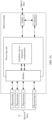
- FIG. 2A is a schematic diagram of a structure of an optical module.
- the optical module includes an optoelectronic transceiver (TX/RX for short), a controller, and a processing unit.
- the controller is configured to control the optoelectronic transceiver and the processing unit to perform various operations.
- the controller may be a micro-controller unit (micro-controller unit, MCU).
- the processing unit may be configured to: encode and decode a digital signal/analog signal, and perform compensation for a plurality of costs in a transmission link, for example, dispersion compensation in long-distance transmission.
- the processing unit may further include a bit multiplexer/demultiplexer (referred to as BitMux in this application).
- the BitMux is configured to map signals received over N physical lanes to an internal processing lane in the processing unit. There may be one or more internal processing lanes.
- the processing unit may be, for example, an optical digital signal processor (optical digital signal processor, oDSP).
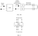
- FIG. 2B is a schematic diagram of an operating circuit of the oDSP. In a transmit direction, a digital signal is processed by the oDSP and converted into an analog modulated electrical signal by using a modulation algorithm.
- the modulation algorithm may be cross-quadrature amplitude modulation (cross-quadrature amplitude modulation, XQAM).
- the analog modulated electrical signal is processed by an optical transmitter TX, and is then converted into a modulated optical signal; and the modulated optical signal is sent.
- the optical signal is processed by an optical receiver, and is then converted into an analog modulated electrical signal.
- the analog modulated electrical signal is processed by the oDSP and is then converted into a digital signal.
- a network device when a network device serves as a transmitting end, the network device receives data, and a MAC layer of the network device forms an Ethernet frame based on a received data stream. Then, the Ethernet frame is sent to a PCS.
- the PCS performs code block encoding on the data, and sends encoded data to a plurality of logical lanes in the PCS.
- the encoded data is sent to a PMA over the plurality of logical lanes.
- bit mux bit multiplexing
- the PMA distributes the data to one or more physical lanes.
- the data on the one or more physical lanes is processed by a PMD sublayer, and is then converted into an analog signal. Then, the analog signal is sent to a transmission medium through a media dependent interface (MDI). Processing in the receive direction is in reverse to that in the transmit direction.
- MDI media dependent interface
- the foregoing logical lanes may also be referred to as virtual lanes (virtual lanes), and in this application, are referred to as PCS lanes or forward error correction (forward error correction, FEC) lanes (referred to as the FEC lanes in a 100 GB standard, and the PCS lanes in a 200 GB/400 GB standard).
- FEC forward error correction
- These lanes are generally distributed inside an implementation unit of the PCS. For example, in a 200 GB Ethernet, eight PCS lanes or FEC lanes are specified; in a 400 GB Ethernet, 16 logical lanes are specified; and in a 100 GB Ethernet, four logical lanes are specified.
- the foregoing physical lane means a PMA lane.
- One physical lane may carry data of one or more logical lanes. In the 100 GB/200 GB/400 GB high-speed Ethernet, a quantity of physical lanes varies based on different implementations.
- bit multiplexing is a function, applicable to counting of all input/output lanes and transmission in all directions.
- Data streams (data streams)/data bits (data bits) received over m input lanes may be sent to n output lanes in a bit interleaving mode.
- FIG. 3 is a schematic diagram of a bit multiplexing process. In FIG. 3 , bit multiplexing is performed on signal streams of four input lanes at a PMA sublayer, and signal streams obtained through the bit multiplexing are sent to two output lanes.
- an alignment marker (alignment marker, AM) is designed in the IEEE 802.3 standard.
- AM alignment marker
- a PCS at a transmitting end periodically inserts AMs into a data stream of each PCS lane.
- the receiving end performs AM lock based on the AMs of each lane (that is, locks a lane corresponding to the AMs), so that a plurality of signals are combined into one serial signal.
- Formats of alignment markers corresponding to different transmission rates may be different. Formats of AMs in 200 GB/s and 400 GB/s are shown in FIG. 4 .
- CM 0 , CM 1 , CM 2 , CM 3 , CM 4 , and CM 5 are common markers of all logical lanes, and UM 0 , UM 1 , UM 2 , UM 3 , UM 4 , and UM 5 are used to uniquely identify a logical lane, that is, different logical lanes have different combinations of "UM 0 , UM 1 , UM 2 , UM 3 , UM 4 , and UM 5 ".
- UP 0 , UP 1 , and UP 2 fields are editable by a user.
- Lengths of AMs in 200 GB and 400 GB are 120 bits (bits), and the bits are arranged at 0 to 119 positions (positions).
- ⁇ CM 0 , CM 1 , CM 2 ⁇ , ⁇ CM 3 , CM 4 , CM 5 ⁇ , ⁇ UM 0 , UM 1 , UM 2 ⁇ , and ⁇ UM 3 , UM 4 , UM 5 ⁇ each occupy 24 bits
- ⁇ UP 0 ⁇ , ⁇ UP 1 ⁇ , and ⁇ UP 2 ⁇ each occupy 8 bits.
- 200 GB corresponds to eight logical lanes
- 400 GB corresponds to 16 logical lanes.
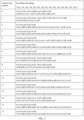
- the 400 GB lanes are used as an example, and an encoding structure of an alignment marker of each logical lane is shown in FIG. 5 .
- CM 0 to CM 5 are divided into 12 symbols, and each symbol occupies 4 bits (namely, a nibble, nibble).
- the receiving end compares CM 0 to CM 5 in a received AM with CM 0 to CM 5 in FIG. 5 . Only when the received AM has less than or equal to 3 nibbles that do not match those of CM 0 to CM 5 in FIG. 5 , a logical lane may be locked, and a logical lane number (number) may be correctly identified.
- an encryption protocol MACsec is proposed in this field.
- the encryption protocol MACsec runs at a MAC layer, and can implement integrity and confidentiality of connectionless data based on a media access independent protocol.
- MACsec uses an advanced encryption standard (Advanced Encryption Standard, AES) for encrypting groups by using a symmetric key, to generate encrypted data.
- AES Advanced Encryption Standard
- Grouping means that plaintext (plaintext) is divided into different groups. Lengths of all group are the same.
- One group of data is encrypted at one time until the entire plaintext is encrypted.
- the length of the group may be 128 bits, 192 bits, 256 bits, or the like.
- ICV Integrity Check Value
- IV Initialization Vector
- MACsec implements data encryption and decryption based on an Ethernet data link layer (layer 2), with an improvement in system capacity and an increase in port bandwidth, a high-speed and large-capacity chip requires increasingly higher power consumption to implement the MACsec function.
- impact of a delay of a new service becomes more obvious.
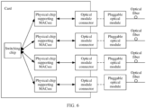
- a physical chip supporting a MACsec function is usually disposed outside a switching chip of a network device in the industry.
- the MACsec function may also be implemented by the switching chip.
- the switching chip may be deployed on a card (also referred to as a line card).
- the implementation is closely related to board hardware, regardless of whether the implementation is based on the physical chip or the switching chip. Therefore, the implementation fails to meet a requirement of a customer for implementing MACsec encryption and decryption based on an existing conventional board.
- a port encryption requirement of a user an individual or entity that has purchased and used a network device
- a demand at time of purchasing the network device can be met provided that there are eight fixed ports supporting the MACsec function. If more MACsec ports are required in subsequent application, it is necessary to update hardware and increase investment. If MACsec ports on the purchased network device are far more than ports that are actually needed, excessive investment may occur. Therefore, for an existing conventional hardware system or a dynamic change in the site application, this solution fails to meet the requirement of the customer.
- an optical module encryption solution shown in FIG. 7 is provided in this application. Because an optical module may be independent of a board, a user only needs to purchase an optical module supporting encryption, and a new encryption requirement can be met.
- a modifiable field of an AM is used to carry an encryption parameter, without adding extra bandwidth.
- the foregoing modifiable field may be, for example, one or more of fields UP 0 , UP 1 , and UP 2 (which are collectively referred to as a UP x field in this application) in a 200 GB or 400 GB AM.
- padding (padding) information may be inserted at a specific position of a data stream to carry the encryption parameter.
- AM lock has been completed at both an encryption side device and a decryption side.
- the AM lock means that when two consecutive AMs are found from a data stream on a logical lane, and the two consecutive AMs match AMs of the lane (that is, the two consecutive AMs are the same as the AMs of the lane or a comparison result of the two consecutive AMs and the AMs of the lane meets a matching rule), it is considered that the lane is locked.
- an operation for example, inserting the encryption parameter or aligning lanes
- Alignment is used to compensate for a deviation caused by transmission over different lanes, so that a receiving end performs corresponding processing only after receiving a complete data block from the lanes.
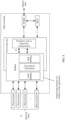
- FIG. 8 is a schematic diagram of a structure of an improved optical module according to this application.
- the optical module includes a controller, a processing unit, and TX/RX. Further, the optical module further includes BitMux to perform a bit multiplexing function.
- the BitMux may be deployed on or outside the processing unit.
- the BitMux may include two sub-bit multiplexing functions: N:M BitMux and M:K BitMux.
- N (N ⁇ 1) is a quantity of external physical lanes
- M (M ⁇ 1) is a quantity of internal virtual lanes of the BitMux
- K (K ⁇ 1) is a quantity of physical lanes supported by the optical module.
- the BitMux further includes an encryption/decryption component.
- the optical module receives N physical lane data streams transmitted by a PMD (or another electrical chip) at a physical layer.
- the N:M BitMux converts the N physical lane data streams input to the optical module into M logical lane data streams.
- the encryption/decryption component identifies an AM of each logical lane from the M logical lane data streams, adds an encryption parameter to the AM of each logical lane, and encrypts a data message to obtain encrypted M data streams.
- the M:K BitMux multiplexes the encrypted M logical lane data streams to K data streams at K physical lanes of the processing unit.
- the processing unit performs algorithm processing (for example, dispersion compensation preprocessing, optionally) on the K data streams. Then, processed K data streams are converted into optical signals by the TX, and the optical signals are sent to another optical module. When applied to a receiving end, the optical module receives an optical signal from another optical module, where the optical signal carries an encrypted data stream. The optical signal is converted into an electrical signal by the RX.
- the processing unit performs algorithm processing (for example, dispersion compensation) on the electrical signal to obtain a digital signal, and sends the digital signal to the M:K BitMux over the K physical lanes.
- the M:K BitMux converts K physical lane data streams into M logical lane data streams.
- the encryption/decryption component identifies AMs in the M logical lane data streams, obtains encryption parameters in the data streams, decrypts the M logical lane data streams to obtain decrypted M data streams, and sends the decrypted M data streams to the N:M BitMux over the M logical lanes.
- the N:M BitMux converts the received M logical lane data streams into N physical lane data streams, and transmits the N physical lane data streams to the PMD or another electrical chip at the physical layer.
- this application provides a status notification method and a related apparatus, to enable a network device (that is, a device located at either end of a lane, which may be the encryption side device or the decryption side device) to obtain an AM lock status of the lane, and determine, based on the AM lock status of the lane, whether an encryption/decryption operation can be performed.
- the AM lock status of the lane may be AM lock statuses of all lanes between devices at both ends, or an AM lock status of one lane.
- a device at one end of the lane is a local end
- a device at the other end of the lane is a peer end.
- the AM lock status of the lane includes: A local end AM is not locked, and a peer end AM is not locked; a local end AM is not locked, and a peer end AM is locked; a local end AM is locked, and a peer end AM is not locked; and a local end AM is locked, and a peer end AM is locked.
- the status notification method according to this application may be applied to a scenario shown in FIG. 9 .
- an edge node A is connected to an edge node D through intermediate nodes B and C. Based on the Ethernet, the edge node A is connected to the intermediate node B, the intermediate node B is connected to the intermediate node C, and the intermediate node C is connected to the edge node D.
- the status notification method in this application is applicable.
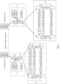
- the network system includes a first network device 100 and a second network device 200.
- the first network device 100 and the second network device 200 may be any two of the nodes in FIG. 9 .
- the first network device 100 includes a first optical module 1010
- the second network device includes a second optical module 2010.
- the first optical module 1010 of the first network device 100 is connected to the second optical module 2010 of the second network device 200.
- An encryption/decryption component of the first optical module 1010 further includes a status determining unit 1011, a notification unit 1012, an encryption/decryption unit 1013, M logical lanes (referred to as transmitting logical lanes in this application) in a transmit direction, and M logical lanes (referred to as receiving logical lanes in this application) in a receive direction.
- the second optical module 2010 and the first optical module 1010 have similar structures and functions. For brevity, this application merely shows a schematic diagram of a structure of the encryption/decryption component in the first optical module 1010. Implementations of the status determining unit 1011, the notification unit 1012, and the encryption/decryption unit 1013 are not limited in this application.
- the first optical module 1010 determines a lock status of a logical lane of the first optical module 1010, sends first uplink notification information to the second optical module 2010 of the second network device 200 after the logical lane of the first optical module 1010 is locked (for ease of description, in this application, a direction from the first network device 100 to the second network device 200 is referred to as an uplink direction; a direction from the second network device 200 to the first network device 100 is referred to as a downlink direction; and correspondingly, notification information sent from the first network device 100 to the second network device 200 is referred to as uplink notification information, and notification information sent from the second network device 200 to the first network device 100 is referred to as downlink notification information), or triggers a processing component 1020 (deployed outside the optical module 1010) of the first network device 100 to send second uplink notification information or third uplink notification information to the second network device.
- a processing component 1020 deployed outside the optical module 1010
- the first uplink notification information, the second uplink notification information, or the third uplink notification information is used to enable the second optical module 2010 to determine that the logical lane of the first optical module 1010 is locked.
- the first optical module 1010 or the second optical module 2010 performs a corresponding encryption/decryption operation only after determining that logical lanes of both a local end and a peer end are locked.
- the first network device is used as an encryption side device
- the second network device is used as a decryption side device, and vice versa.
- the following uses an example in which the first network device is a transmitting end (the encryption side device) and the second network device is a receiving end (the decryption side device) to describe a status notification method of this application in detail.
- FIG. 11 is a schematic flowchart of the status notification method according to this application, and the method includes steps S101 to S104. The method is performed by the first optical module 1010 or the first network device 100 shown in FIG. 10A to FIG. 10C .
- step S101 a lock status of a logical lane in the first optical module is determined.
- the first optical module 1010 receives N physical lane signals over the N physical lanes in FIG. 10A to FIG. 10C , and converts, by using N:M BitMux, the N physical lane signals into M logical lane signals that are respectively transmitted over the M transmitting logical lanes, where each logical lane signal includes alignment markers inserted at spacing by a PCS of the first network device 100.
- the first optical module receives K physical lane signals over the K physical lanes in FIG. 10A to FIG. 10C , and converts, by using M:K BitMux, the K physical lane signals into M logical lane signals that are respectively transmitted over the M receiving logical lanes, where each logical lane signal includes alignment markers inserted by a PCS of the second network device.
- the determining a lock status of a logical lane in the first optical module includes: determining a status of each transmitting logical lane in the M transmitting logical lanes; or determining a status of each logical lane in the M transmitting logical lanes and the M receiving logical lanes.
- the status of each logical lane includes a locked state or an unlocked state. That the logical lane is locked means that alignment markers that meet a matching rule exist on the logical lane, and positions of the alignment markers can be accurately identified. After the logical lane is locked, data can be transmitted over the logical lane.
- Step S101 may be specifically performed by the status determining unit 1011 of the first optical module 1010.
- the status determining unit 1011 of the first optical module 1010 determines the status of each transmitting logical lane in the M transmitting logical lanes in the following manner.
- a format (format) of the first alignment marker may be the same as that of an alignment marker used in a 200 GB/400 GB lane shown in FIG. 4 .
- the status determining unit 1011 determines the status of the transmitting logical lane i based on the first alignment marker, where the status of the transmitting logical lane i includes a locked state or an unlocked state.
- the status determining unit 1011 of the first optical module 1010 determines the status of each receiving logical lane in the M receiving logical lanes in the following manner.
- a format (format) of the second alignment marker may be the same as that of the alignment marker used in the 200 GB/400 GB lane shown in FIG. 4 . That is, formats of the second alignment marker and the first alignment marker are the same.
- the status determining unit 1011 determines a status of the receiving logical lane q based on the second alignment marker, where the status of the receiving logical lane q includes a locked state or an unlocked state.
- a method for determining the status of the transmitting logical lane i based on the first alignment marker is the same as a method for determining the status of the receiving logical lane q based on the second alignment marker.
- the following uses an example in which the status of the transmitting logical lane i is determined based on the first alignment marker to describe how to determine a status of a logical lane.
- the transmitting logical lane i is locked.
- the transmitting logical lane i is not locked.
- a corresponding reference alignment marker is provided for each transmitting logical lane.
- the reference alignment marker may be an alignment marker specified in the IEEE 802.3 standard, or may be an alignment marker in another format used to determine whether a logical lane is locked.
- M when M is 16, a reference alignment identifier of each logical lane may be shown in FIG. 5 .
- That the first alignment marker matches the reference alignment marker of the transmitting logical lane i means that the first alignment marker is the same as the reference alignment marker, that a quantity of bits that are of the first alignment marker and that are inconsistent with those of the reference alignment marker is less than or equal to a specified threshold (for example, values of two bits of the first alignment marker are allowed to be different from those of corresponding bits of the reference marker), or that a quantity of bits that are of the first alignment marker and that are the same as those of the reference alignment marker reaches a specified proportion (for example, values of 98% or more bits in the first alignment marker are the same as those of corresponding bits in the reference alignment marker).
- a specified threshold for example, values of two bits of the first alignment marker are allowed to be different from those of corresponding bits of the reference marker
- a specified proportion for example, values of 98% or more bits in the first alignment marker are the same as those of corresponding bits in the reference alignment marker.
- Step S101 is performed, so that the first optical module 1010 (for example, the status determining unit 1011 of the first optical module 1010) determines the status of each logical lane in the M transmitting logical lanes and the M receiving logical lanes in first optical module.
- the first network device 100 (for example, specifically, the processing component of the first network device 100) may also obtain, from the first optical module 1010, the lock status of each logical lane in the first optical module 1010.
- the status determining unit 1011 of the first optical module 1010 may send the lock status of each logical lane to the first network device 100 in real time.
- the status determining unit 1011 of the first optical module 1010 may also send lock statuses of all the M transmitting logical lanes and the M receiving logical lanes to the first network device 100 at one time.
- the first network device 100 may also poll each logical lane of the first optical module 1010 to obtain the lock status of each logical lane in real time.
- a manner in which the first network device 100 obtains the lock status of the logical lane in the first optical module 1010 is not limited in this application.
- step S102 uplink notification information is sent when the lock status indicates that the logical lane in the first optical module is locked.
- the uplink notification information is used to enable the second optical module to determine that the logical lane in the first optical module is locked, the second optical module belongs to the second network device, and the first optical module is connected to the second optical module. Based on different scenarios, the uplink notification information may be first uplink communication information, second uplink notification information, or third uplink notification information, which is described in detail below.
- the first optical module 1010 or the first network device 100 After the first optical module 1010 or the first network device 100 obtains lock statuses of all logical lanes in the first optical module 1010, the first optical module 1010 or the first network device 100 determines, based on a preset rule, whether the logical lane in the first optical module is locked (step S1011). If the logical lane is not locked, step S101 is performed; and if the logical lane is locked, step S102 is performed.
- the preset rule is used to determine whether the logical lane in the first optical module is locked. To be specific, when the preset rule is met, the logical lane in the first optical module is locked; and when the preset rule is not met, the logical lane in the first optical module is not locked.
- the preset rule includes any one or more of the following.
- the M transmitting logical lanes are all locked, and/or the M transmitting logical lanes are locked; one of the M transmitting logical lanes is locked;
- mapping relationships need to be configured on the first optical module 1010 or the first network device 100.
- the mapping relationships record a correspondence between the transmitting logical lane and the receiving logical lane on the first optical module 1010.
- the mapping relationship may further include a correspondence between a transmitting logical lane and a receiving logical lane on the second optical module 2010.
- A represents a logical lane on the first optical module
- B represents a logical lane on the second optical module
- T represents a transmitting logical lane
- R represents a receiving logical lane
- a numeral represents a logical lane number.
- Table 1 AT0 AR1 BT1 BR2 AT1 AR3 BT0 BR1 AT2 AR2 BT3 BR3 ... ... ... ... ...
- step S102 further includes the following implementations.
- Manner 1 If the preset rule is that the M transmitting logical lanes are all locked, and/or the M receiving logical lanes are all locked, the first optical module 1010 sends, when the preset rule is met, M pieces of first uplink notification information to the second optical module 2010 respectively over the M transmitting logical lanes. That is, one piece of first uplink notification information is sent over one transmitting logical lane, where each piece of first uplink notification information indicates that the transmitting logical lane for sending the first uplink notification information is locked, and/or indicates that a receiving logical lane corresponding to the transmitting logical lane of the first uplink notification information is locked.
- Manner 2 If the preset rule is that the M transmitting logical lanes are all locked, and/or the M transmitting logical lanes and the M receiving logical lanes are all locked, when the preset rule is met, the processing component 1020 of the first network device sends, second uplink notification information to a processing component 2020 of the second network device, where the second uplink notification information indicates that the M transmitting logical lanes of the first optical module are all locked and/or the M receiving logical lanes are all locked.
- Manner 3 If the preset rule is that one of the M transmitting logical lanes is locked, one of the M receiving logical lanes is locked, or one of the M transmitting logical lanes and a corresponding receiving logical lane are locked, when the preset rule is met, it is assumed, that j transmitting logical lanes in the M transmitting logical lanes are locked, receiving lanes corresponding to the j transmitting logical lanes are locked, or the j transmitting logical lanes and the corresponding logical lanes are locked.
- the first optical module 1010 sends first uplink notification information to the second optical module over the j transmitting logical lanes, where the first uplink notification information indicates that the j transmitting logical lanes are locked, that receiving logical lanes corresponding to the j transmitting logical lanes are locked, or that the j transmitting logical lanes and the corresponding receiving logical lanes are locked; j is greater than 1 and less than M; and when the j transmitting logical lanes includes a plurality of transmitting logical lanes, each transmitting logical lane corresponds to one piece of first uplink notification information.
- Manner 4 If the preset rule is that one or more of the M transmitting logical lanes are locked, one or more of the M receiving logical lanes are locked, or one or more of the M transmitting logical lanes and corresponding receiving logical lanes are locked, when the preset rule is met, it is assumed, that j transmitting logical lanes in the M transmitting logical lanes are locked, receiving lanes corresponding to the j transmitting logical lanes are locked, or the j transmitting logical lanes and the corresponding logical lanes are locked.
- the processing component 1020 of the first network device 100 sends third uplink notification information to a processing component 2020 of the second network device 200, where the third uplink notification information indicates that the j transmitting logical lanes are locked, that the receiving lanes corresponding to the j transmitting logical lanes are locked, or that the transmitting logical j and the corresponding receiving logical lanes are locked; and j is greater than 1 and less than M.
- the first uplink notification information, the second uplink notification information, or the third uplink information may indicate lock of a logical lane in different scenarios.
- the information may be configured as required to specifically indicate a scenario of logical lane lock.
- a format of the first uplink notification information in the foregoing manner 1 is the same as that of the first uplink notification information in the foregoing manner 3.
- Each piece of first uplink notification information includes an identifier of a transmitting logical lane for sending the first uplink notification information, and a lock flag.
- the lock flag indicates that the transmitting logical lane of the first uplink notification information is locked.
- First uplink notification information transmitted over different transmitting logical lanes includes different lane identifiers.
- the first uplink notification information transmitted over the different transmitting logical lanes may include a same lock flag.
- the lock flag is obtained by modifying a specified field in the alignment marker.
- the lock flag may appear for one time or repeatedly for a plurality of times. When the lock flag appears repeatedly for a plurality of times, it can ensure that a receiving end correctly identifies the lock flag.
- the foregoing first uplink notification information may be obtained by modifying the alignment marker shown in FIG. 4 or FIG. 5 , or may be obtained by modifying a specified field in an alignment marker of another format. For example, when the first optical module is a 200 GB/400 GB optical module, values of one or more fields of UP 0 , UP 1 , and UP 2 in the alignment marker (namely, the reference alignment marker) of the transmitting logical lane shown in FIG.
- modified ⁇ UP 0 , UP 1 , UP 2 ⁇ is used as a lock flag to indicate that one transmitting logical lane is locked, the M transmitting logical lanes are all locked, or the M transmitting logical lanes and the M receiving logical lanes are locked.
- lock flags of M pieces of first uplink communication information respectively transmitted over the M transmitting logical lanes are the same.
- a format of the second uplink notification information in the foregoing manner 2 may be the same as or different from that of the third uplink notification information in the foregoing manner 4.
- the foregoing second uplink notification information and the third uplink notification information may be carried in a layer 2 Ethernet frame or an IP data packet.
- the first network device 100 may notify, by using one piece of second uplink notification information, that the transmitting logical lanes are all locked/or the receiving logical lanes are all locked.
- the first network device 100 may send the third uplink notification information when determining that one or more transmitting logical lanes are locked and one or more receiving logical lanes are locked, or determining that one transmitting logical lane and a corresponding receiving logical lane are locked.
- the first optical module 1010 or the first network device 100 may enable the second optical module 2010 to obtain lock statuses of logical lanes in the first optical module 1010.
- the status determining unit 1011 may determine whether the lock status of the logical lane in the first optical module 1010 meets the preset rule, and trigger, when the lock status of the logical lane in the first optical module 1010 meets the preset rule, the notification unit 1012 to send the first uplink notification information.
- the notification unit 1012 may determine, based on a lock status that is of the logical lane in the first optical module 1010 and that is detected by the status determining unit 1011, whether the lock status of the logical lane in the first optical module 1010 meets the preset rule.
- step S103 the first network device or the first optical module obtains downlink notification information, where the downlink notification information is used to enable the first optical module to determine that a logical lane in the second optical module is locked.
- the downlink notification information is sent by the second network device 200 or the second optical module 2010.
- a generation condition and a sending mode of the downlink notification information are similar to those of the foregoing uplink notification information. Examples are as follows.
- the first optical module 1010 receives M pieces of first downlink notification information over the M receiving logical lanes, where the M pieces of first downlink notification information indicate that a logical lane in the second optical module 2010 is locked. That a logical lane in the second optical module 2010 is locked includes that M receiving logical lanes and M transmitting logical lanes of the second optical module 2010 are locked.
- the processing component 1020 of the first network device 100 receives second downlink notification information sent by the processing component 2020 of the second network device 200, and sends the second downlink notification information to the first optical module 1010, where the second downlink notification information indicates that a logical lane in the second optical module 2010 is locked. That a logical lane in the second optical module 2010 is locked includes that M receiving logical lanes and M transmitting logical lanes of the second optical module 2010 are locked.
- the first optical module 1010 receives first downlink notification information over p receiving logical lanes in the M receiving logical lanes, where the first downlink notification information indicates that transmitting logical lanes and receiving logical lanes that are of the second optical module 2010 and that correspond to the p receiving logical lanes are locked, p is greater than 1 and less than M, and when the p receiving logical lanes include a plurality of receiving logical lanes, each receiving logical lane corresponds to one piece of first downlink notification information.
- the processing component 1020 of the first network device 100 receives third downlink notification information sent by the processing component 2020 of the second network device 200, and sends the third downlink notification information to the first optical module 1010, where the second downlink notification information indicates that transmitting logical lanes and receiving logical lanes that are of the second optical module 2010 and that correspond to p receiving logical lanes are locked, and p is greater than 1 and less than M.
- the second optical module 2010 is a receiving end, and the second optical module 2010 may return data to the first optical module 1010. This indicates that the receiving logical lane of the second optical module is definitely locked. Therefore, in the scenario 1 and the scenario 2, the M pieces of first downlink notification information and the second downlink notification information indicate that the M receiving logical lanes and the M transmitting logical lanes of the second optical module 2010 are all locked. In the scenario 3 and the scenario 4, the first downlink notification and the third downlink notification indicate that the transmitting logical lanes and receiving logical lanes that are of the second optical module 2010 and that correspond to the p receiving logical lanes are locked.
- the first downlink notification information in the foregoing scenario 1 and the scenario 3 may be received by the status determining unit 1012 in the first optical module 1010.
- the second downlink notification information in the foregoing scenario 2 and the third downlink notification information in the foregoing scenario 4 may be received by the processing component 1020 in the first network device 100, and sent to the status determining unit 1012 in the first optical module 1010.
- the processing component 1020 may convert the second downlink notification information and the fourth downlink notification information into a format that can be recognized by the status determining unit 1012 of the first optical module 1010, and then send the converted second downlink notification information and the converted fourth downlink notification information.
- the foregoing second downlink notification information and the third downlink notification information may be carried in a layer 2 Ethernet frame or an IP data packet.
- step S104 after the logical lane in the first optical module is locked and the logical lane in the second optical module is locked, the first optical module processes data. Specifically, the first optical module encrypts data sent to the second optical module, or the first optical module decrypts data received from the second optical module. The processing may further include inserting handshake information into the data, and the like.
- Step S104 may be performed by the encryption/decryption unit 1013 in the first optical module 1010, and the data encryption operation or the data decryption operation in step S104 is only a data processing manner.
- the first optical module 1010 may further include another processing unit.
- step S104 may be replaced with another data processing operation.
- the following describes application of the status notification method provided in embodiments of this application with reference to the alignment marker formats in FIG. 4 and FIG. 5 and the schematic diagram of the data transmission process in FIG. 12 .
- the PCS of the first network device 100 When the first network device 100 transmits data to the second network device 200, as shown in FIG. 12 , the PCS of the first network device 100 periodically inserts AMs into a data stream, and the AMs inserted by the PCS are the standard AMs shown in FIG. 4 or FIG. 5 .
- the status determining unit of the first optical module 1010 detects a status of each transmitting logical lane and each receiving logical lane of the first optical module in real time.
- the first optical module 1010 sends the data stream to the M transmitting logical lanes, identifies, for each transmitting logical lane and/or receiving logical lane, the AM in the data stream transmitted over the transmitting logical lane and/or the receiving logical lane, and determines, based on the AM, and a reference AM (the reference AM is the AM listed in FIG.
- the first optical module 1010 When the logical lane in the first optical module 1010 is not locked, the first optical module sends the standard AM inserted by the PCS (that is, the first optical module directly sends the AM without modifying the AM).
- the first optical module modifies the obtained AM, so that modified AM carries a lock flag.
- the AM is the AM shown in FIG. 5 .
- the lock flag is obtained by modifying a UP x field in the AM shown in FIG. 5 .
- the UP x field may be one or more of the UP 0 , the UP 1 , and the UP 2 .
- the lock flag may occupy one or more bits, and a value of the lock flag may be set, for example, the lock flag may be "01" or "0011".
- the lock flag may be repeatedly transmitted (that is, the lock flag repeatedly appears in the AM). For example, in FIG. 12 , if the lock flag is "01 ", values of UP 0 , UP 1 , and UP 2 are all "01010101". In this way, the lock flag may be transmitted for 12 times by using one AM, and a probability that the lock flag is incorrect is low.
- bit error rate bit error ratio
- a probability that an AMlock bit sequence is correct is P 2 .
- a time periodicity in which the AMs appear on each lane is considered, and an error occurs in the bit sequence in about ten thousand years. Therefore, the reliability is high.
- the first optical module 101 modifies a first AM that is obtained after the logical lane is locked and that corresponds to the logical lane, so that the AM includes a multiframe flag.
- the multiframe flag indicates that data transmitted after the AM is processed data.
- the multiframe flag may occupy one or more bits, and the multiframe flag is different from the lock flag.
- the multiframe flag may also appear repeatedly in the AM, to improve transmission reliability. As shown in FIG. 12 , if the multiframe is marked as "10", values of UP 0 , UP 1 , and UP 2 are all "01010101".
- An AM following the AM that includes the multiframe flag may include encryption information such as a key and an IV, so that after receiving a data stream, the second optical module 2010 decrypts the data stream based on the key and the IV
- FIG. 13 is a schematic diagram of another data transmission process according to this embodiment of this application. Different from FIG. 12, FIG. 13 does not include a multiframe flag.
- the first optical module 1010 modifies each AM that is obtained after the logical lanes are locked and that corresponds to the logical lane, so that the AM includes an encryption flag.
- the encryption flag indicates that a data stream after the AM is an encrypted data stream.
- the second optical module 2010 decrypts the data stream.
- multiframe flag and the encryption flag in FIG. 12 and FIG. 13 may also be replaced with other information, so that the optical module implements more operations.
- the lock status of the logical lane in the optical module may be indicated without increasing the transmission bandwidth of the network device.
- the optical module performs encryption/decryption or another operation after the logical lanes at the local end and the peer end are locked, thereby improving operation reliability.
- the encryption/decryption component in the first optical module 1011 in this application may be implemented by software, or may be implemented by hardware.
- the encryption/decryption component may be implemented by an independent chip, or may be implemented by a logic circuit.
- the chip or the logic circuit may be integrated into the optical module.
- a plurality of mentioned in embodiments of this application means two or more.
- the term “and/or” describes an association relationship for describing associated objects and represents that three relationships may exist.
- a and/or B may represent the following three cases: Only A exists, both A and B exist, and only B exists.
- the character “/” generally indicates an "or" relationship between the associated objects.
- Names or numbers of steps in this application do not mean that the steps in the method procedure need to be performed in a time/logical sequence indicated by the names or numbers.
- An execution sequence of the steps in the procedure that have been named or numbered can be changed based on a technical objective to be achieved, provided that same or similar technical effects can be achieved.
- Division into units in this application is logical division. During actual application, there may be another division manner. For example, a plurality of units may be combined or integrated into another system, or some features may be ignored or not performed.
- the displayed or discussed mutual couplings or direct couplings or communication connections may be implemented through some interfaces.
- the indirect couplings or communication connections between the units may be implemented in electrical or other similar forms. This is not limited in this application.
- units or subunits described as separate parts may or may not be physically separate, may or may not be physical units, or may be distributed into a plurality of circuit units. All or a part of the units may be selected based on actual requirements to achieve the objectives of the solutions of this application.
Landscapes
- Engineering & Computer Science (AREA)
- Computer Security & Cryptography (AREA)
- Computer Networks & Wireless Communication (AREA)
- Signal Processing (AREA)
- Computer Hardware Design (AREA)
- Computing Systems (AREA)
- General Engineering & Computer Science (AREA)
- Physics & Mathematics (AREA)
- Electromagnetism (AREA)
- Small-Scale Networks (AREA)
Applications Claiming Priority (3)
| Application Number | Priority Date | Filing Date | Title |
|---|---|---|---|
| CN202110021317 | 2021-01-08 | ||
| CN202110363540.6A CN114760544A (zh) | 2021-01-08 | 2021-04-02 | 一种物理层状态通知方法、光模块、网络设备以及网络系统 |
| PCT/CN2021/139424 WO2022148230A1 (fr) | 2021-01-08 | 2021-12-18 | Procédé de notification d'état, module optique, dispositif de réseau et système de réseau |
Publications (3)
| Publication Number | Publication Date |
|---|---|
| EP4262093A1 true EP4262093A1 (fr) | 2023-10-18 |
| EP4262093A4 EP4262093A4 (fr) | 2024-06-05 |
| EP4262093B1 EP4262093B1 (fr) | 2025-05-21 |
Family
ID=82326236
Family Applications (1)
| Application Number | Title | Priority Date | Filing Date |
|---|---|---|---|
| EP21917270.7A Active EP4262093B1 (fr) | 2021-01-08 | 2021-12-18 | Procédé de notification d'état, module optique, dispositif de réseau et système de réseau |
Country Status (4)
| Country | Link |
|---|---|
| US (1) | US12537607B2 (fr) |
| EP (1) | EP4262093B1 (fr) |
| CN (1) | CN114760544A (fr) |
| WO (1) | WO2022148230A1 (fr) |
Families Citing this family (3)
| Publication number | Priority date | Publication date | Assignee | Title |
|---|---|---|---|---|
| CN117675101A (zh) * | 2022-09-08 | 2024-03-08 | 华为技术有限公司 | 数据传输方法、装置、系统及计算机可读存储介质 |
| CN117040843B (zh) * | 2023-08-10 | 2025-03-04 | 昆高新芯微电子(江苏)有限公司 | 多DP交换芯片实现MACsec的方法和装置 |
| CN120034289A (zh) * | 2023-11-21 | 2025-05-23 | 华为技术有限公司 | 前向纠错模式通告方法、装置、设备、系统及存储介质 |
Family Cites Families (12)
| Publication number | Priority date | Publication date | Assignee | Title |
|---|---|---|---|---|
| US8370704B2 (en) * | 2009-03-09 | 2013-02-05 | Intel Corporation | Cable interconnection techniques |
| US8307265B2 (en) * | 2009-03-09 | 2012-11-06 | Intel Corporation | Interconnection techniques |
| KR101250538B1 (ko) * | 2009-06-26 | 2013-04-03 | 한국전자통신연구원 | 이더넷 장치 및 이더넷 장치의 레인 운용 방법 |
| KR101238917B1 (ko) * | 2009-11-12 | 2013-03-06 | 한국전자통신연구원 | 이더넷 장치 및 그의 전송률 조절 방법 |
| US9692715B2 (en) * | 2014-02-21 | 2017-06-27 | Cavium, Inc. | Multiple ethernet ports and port types using a shared data path |
| US9413454B1 (en) * | 2014-06-30 | 2016-08-09 | Juniper Networks, Inc. | Automatic bandwidth adjustment on multi-fiber optics |
| US9876709B1 (en) * | 2014-08-28 | 2018-01-23 | Xilinx, Inc. | Alignment detection in a multi-lane network interface |
| US10944478B2 (en) * | 2016-04-12 | 2021-03-09 | Cable Television Laboratories, Inc. | Fiber communication systems and methods |
| US10762731B2 (en) * | 2017-06-13 | 2020-09-01 | United States Postal Service | Mobile device for safe, secure, and accurate delivery of items |
| CN111385678B (zh) * | 2018-12-29 | 2023-05-12 | 中兴通讯股份有限公司 | 一种实现光链路通道自协商的方法和装置 |
| CN117692099A (zh) | 2019-06-04 | 2024-03-12 | 华为技术有限公司 | 一种以太网数据传输的方法和通信设备 |
| US11705694B1 (en) * | 2020-02-26 | 2023-07-18 | Cable Television Laboratories, Inc. | Systems and methods for optical injection-locking in an access network |
-
2021
- 2021-04-02 CN CN202110363540.6A patent/CN114760544A/zh active Pending
- 2021-12-18 WO PCT/CN2021/139424 patent/WO2022148230A1/fr not_active Ceased
- 2021-12-18 EP EP21917270.7A patent/EP4262093B1/fr active Active
-
2023
- 2023-07-10 US US18/349,645 patent/US12537607B2/en active Active
Also Published As
| Publication number | Publication date |
|---|---|
| CN114760544A (zh) | 2022-07-15 |
| EP4262093A4 (fr) | 2024-06-05 |
| US20230353255A1 (en) | 2023-11-02 |
| US12537607B2 (en) | 2026-01-27 |
| EP4262093B1 (fr) | 2025-05-21 |
| WO2022148230A1 (fr) | 2022-07-14 |
Similar Documents
| Publication | Publication Date | Title |
|---|---|---|
| US12537607B2 (en) | Status notification method, optical module, network device, and network system | |
| US12470363B2 (en) | Data transmission method, communication apparatus, and communication system | |
| US7979693B2 (en) | Relay apparatus for encrypting and relaying a frame | |
| JP3774455B2 (ja) | イーサネット(登録商標)受動型光加入者網システムにおけるデータ転送方法 | |
| US20250007691A1 (en) | Data Transmission Method, Device, Readable Storage Medium, and Chip System | |
| CN104426631A (zh) | 对数据进行处理的方法及装置 | |
| KR20080110672A (ko) | 전자 통신에서 적응적 보안 레벨을 제공하는 방법 및 장치 | |
| US12413391B2 (en) | Devices, systems, and methods for integrating encryption service channels with a data path | |
| US20140362989A1 (en) | Securing Virtual Lane Physical Layers | |
| CN107683592A (zh) | 数据处理方法、装置和系统 | |
| US20230269074A1 (en) | Encryption/decryption system, optical module, and related apparatus and system | |
| WO2007099045A1 (fr) | Procédé, système de communication, unité de communication centrale et périphérique pour transfert par paquets de l'information | |
| CN115766046B (zh) | 一种数据传输方法、设备、可读存储介质和芯片系统 | |
| CN111935112B (zh) | 一种基于串行的跨网数据安全摆渡设备和方法 | |
| CN222215742U (zh) | 一种具有加解密通信功能的光模块 | |
| CN114584333A (zh) | 一种数据传输方法、通信装置及通信系统 | |
| EP4645727A2 (fr) | Procédé d'ajustement de débit de transmission, processeur, dispositif de réseau et système de réseau | |
| CN118945644B (zh) | 一种基于编码和加密的数据安全传输方法及电子设备 | |
| CN121603228A (zh) | 数据传输方法、设备、可读存储介质和计算机程序产品 | |
| CN113709172B (zh) | 一种sdh超帧结构及其纠错方法 | |
| KR100798921B1 (ko) | Mac 보안 서비스망에서의 보안 채널 제어 방법 및 이를구현하는 단말 장치 | |
| CN121603229A (zh) | 数据传输方法、装置、设备及存储介质 | |
| WO2026040638A1 (fr) | Procédé et appareil de transmission de données, dispositif et support de stockage | |
| RU16963U1 (ru) | Система защиты пакетов данных в процессе их передачи в выделенном защищаемом фрагменте сети передачи данных общего пользования с коммутацией пакетов, реализующей интернет-протокол, от несанкционированных воздействий | |
| Fiber | IEEE Standard for Ethernet |
Legal Events
| Date | Code | Title | Description |
|---|---|---|---|
| STAA | Information on the status of an ep patent application or granted ep patent |
Free format text: STATUS: THE INTERNATIONAL PUBLICATION HAS BEEN MADE |
|
| PUAI | Public reference made under article 153(3) epc to a published international application that has entered the european phase |
Free format text: ORIGINAL CODE: 0009012 |
|
| STAA | Information on the status of an ep patent application or granted ep patent |
Free format text: STATUS: REQUEST FOR EXAMINATION WAS MADE |
|
| 17P | Request for examination filed |
Effective date: 20230710 |
|
| AK | Designated contracting states |
Kind code of ref document: A1 Designated state(s): AL AT BE BG CH CY CZ DE DK EE ES FI FR GB GR HR HU IE IS IT LI LT LU LV MC MK MT NL NO PL PT RO RS SE SI SK SM TR |
|
| DAV | Request for validation of the european patent (deleted) | ||
| DAX | Request for extension of the european patent (deleted) | ||
| REG | Reference to a national code |
Ref country code: DE Ref legal event code: R079 Ref country code: DE Ref legal event code: R079 Ref document number: 602021031305 Country of ref document: DE Free format text: PREVIOUS MAIN CLASS: H03M0013050000 Ipc: H04B0010250000 |
|
| A4 | Supplementary search report drawn up and despatched |
Effective date: 20240508 |
|
| RIC1 | Information provided on ipc code assigned before grant |
Ipc: H03M 13/05 20060101ALI20240502BHEP Ipc: H04Q 11/00 20060101ALI20240502BHEP Ipc: H04L 9/40 20220101ALI20240502BHEP Ipc: H04B 10/25 20130101AFI20240502BHEP |
|
| GRAP | Despatch of communication of intention to grant a patent |
Free format text: ORIGINAL CODE: EPIDOSNIGR1 |
|
| STAA | Information on the status of an ep patent application or granted ep patent |
Free format text: STATUS: GRANT OF PATENT IS INTENDED |
|
| RIC1 | Information provided on ipc code assigned before grant |
Ipc: H03M 13/05 20060101ALI20241207BHEP Ipc: H04Q 11/00 20060101ALI20241207BHEP Ipc: H04L 9/40 20220101ALI20241207BHEP Ipc: H04B 10/25 20130101AFI20241207BHEP |
|
| INTG | Intention to grant announced |
Effective date: 20250102 |
|
| GRAS | Grant fee paid |
Free format text: ORIGINAL CODE: EPIDOSNIGR3 |
|
| GRAA | (expected) grant |
Free format text: ORIGINAL CODE: 0009210 |
|
| STAA | Information on the status of an ep patent application or granted ep patent |
Free format text: STATUS: THE PATENT HAS BEEN GRANTED |
|
| AK | Designated contracting states |
Kind code of ref document: B1 Designated state(s): AL AT BE BG CH CY CZ DE DK EE ES FI FR GB GR HR HU IE IS IT LI LT LU LV MC MK MT NL NO PL PT RO RS SE SI SK SM TR |
|
| REG | Reference to a national code |
Ref country code: GB Ref legal event code: FG4D |
|
| REG | Reference to a national code |
Ref country code: CH Ref legal event code: EP |
|
| REG | Reference to a national code |
Ref country code: DE Ref legal event code: R096 Ref document number: 602021031305 Country of ref document: DE |
|
| REG | Reference to a national code |
Ref country code: IE Ref legal event code: FG4D |
|
| REG | Reference to a national code |
Ref country code: NL Ref legal event code: MP Effective date: 20250521 |
|
| PG25 | Lapsed in a contracting state [announced via postgrant information from national office to epo] |
Ref country code: PT Free format text: LAPSE BECAUSE OF FAILURE TO SUBMIT A TRANSLATION OF THE DESCRIPTION OR TO PAY THE FEE WITHIN THE PRESCRIBED TIME-LIMIT Effective date: 20250922 Ref country code: ES Free format text: LAPSE BECAUSE OF FAILURE TO SUBMIT A TRANSLATION OF THE DESCRIPTION OR TO PAY THE FEE WITHIN THE PRESCRIBED TIME-LIMIT Effective date: 20250521 Ref country code: FI Free format text: LAPSE BECAUSE OF FAILURE TO SUBMIT A TRANSLATION OF THE DESCRIPTION OR TO PAY THE FEE WITHIN THE PRESCRIBED TIME-LIMIT Effective date: 20250521 |
|
| REG | Reference to a national code |
Ref country code: LT Ref legal event code: MG9D |
|
| PG25 | Lapsed in a contracting state [announced via postgrant information from national office to epo] |
Ref country code: GR Free format text: LAPSE BECAUSE OF FAILURE TO SUBMIT A TRANSLATION OF THE DESCRIPTION OR TO PAY THE FEE WITHIN THE PRESCRIBED TIME-LIMIT Effective date: 20250822 Ref country code: NO Free format text: LAPSE BECAUSE OF FAILURE TO SUBMIT A TRANSLATION OF THE DESCRIPTION OR TO PAY THE FEE WITHIN THE PRESCRIBED TIME-LIMIT Effective date: 20250821 |
|
| PG25 | Lapsed in a contracting state [announced via postgrant information from national office to epo] |
Ref country code: PL Free format text: LAPSE BECAUSE OF FAILURE TO SUBMIT A TRANSLATION OF THE DESCRIPTION OR TO PAY THE FEE WITHIN THE PRESCRIBED TIME-LIMIT Effective date: 20250521 Ref country code: NL Free format text: LAPSE BECAUSE OF FAILURE TO SUBMIT A TRANSLATION OF THE DESCRIPTION OR TO PAY THE FEE WITHIN THE PRESCRIBED TIME-LIMIT Effective date: 20250521 |
|
| PG25 | Lapsed in a contracting state [announced via postgrant information from national office to epo] |
Ref country code: BG Free format text: LAPSE BECAUSE OF FAILURE TO SUBMIT A TRANSLATION OF THE DESCRIPTION OR TO PAY THE FEE WITHIN THE PRESCRIBED TIME-LIMIT Effective date: 20250521 |
|
| PG25 | Lapsed in a contracting state [announced via postgrant information from national office to epo] |
Ref country code: HR Free format text: LAPSE BECAUSE OF FAILURE TO SUBMIT A TRANSLATION OF THE DESCRIPTION OR TO PAY THE FEE WITHIN THE PRESCRIBED TIME-LIMIT Effective date: 20250521 |
|
| PG25 | Lapsed in a contracting state [announced via postgrant information from national office to epo] |
Ref country code: RS Free format text: LAPSE BECAUSE OF FAILURE TO SUBMIT A TRANSLATION OF THE DESCRIPTION OR TO PAY THE FEE WITHIN THE PRESCRIBED TIME-LIMIT Effective date: 20250821 |
|
| PG25 | Lapsed in a contracting state [announced via postgrant information from national office to epo] |
Ref country code: IS Free format text: LAPSE BECAUSE OF FAILURE TO SUBMIT A TRANSLATION OF THE DESCRIPTION OR TO PAY THE FEE WITHIN THE PRESCRIBED TIME-LIMIT Effective date: 20250921 |
|
| PG25 | Lapsed in a contracting state [announced via postgrant information from national office to epo] |
Ref country code: LV Free format text: LAPSE BECAUSE OF FAILURE TO SUBMIT A TRANSLATION OF THE DESCRIPTION OR TO PAY THE FEE WITHIN THE PRESCRIBED TIME-LIMIT Effective date: 20250521 |
|
| REG | Reference to a national code |
Ref country code: AT Ref legal event code: MK05 Ref document number: 1797722 Country of ref document: AT Kind code of ref document: T Effective date: 20250521 |
|
| PGFP | Annual fee paid to national office [announced via postgrant information from national office to epo] |
Ref country code: DE Payment date: 20251104 Year of fee payment: 5 |
|
| PG25 | Lapsed in a contracting state [announced via postgrant information from national office to epo] |
Ref country code: DK Free format text: LAPSE BECAUSE OF FAILURE TO SUBMIT A TRANSLATION OF THE DESCRIPTION OR TO PAY THE FEE WITHIN THE PRESCRIBED TIME-LIMIT Effective date: 20250521 Ref country code: AT Free format text: LAPSE BECAUSE OF FAILURE TO SUBMIT A TRANSLATION OF THE DESCRIPTION OR TO PAY THE FEE WITHIN THE PRESCRIBED TIME-LIMIT Effective date: 20250521 Ref country code: SM Free format text: LAPSE BECAUSE OF FAILURE TO SUBMIT A TRANSLATION OF THE DESCRIPTION OR TO PAY THE FEE WITHIN THE PRESCRIBED TIME-LIMIT Effective date: 20250521 |
|
| PG25 | Lapsed in a contracting state [announced via postgrant information from national office to epo] |
Ref country code: CZ Free format text: LAPSE BECAUSE OF FAILURE TO SUBMIT A TRANSLATION OF THE DESCRIPTION OR TO PAY THE FEE WITHIN THE PRESCRIBED TIME-LIMIT Effective date: 20250521 |
|
| PG25 | Lapsed in a contracting state [announced via postgrant information from national office to epo] |
Ref country code: EE Free format text: LAPSE BECAUSE OF FAILURE TO SUBMIT A TRANSLATION OF THE DESCRIPTION OR TO PAY THE FEE WITHIN THE PRESCRIBED TIME-LIMIT Effective date: 20250521 |
|
| PG25 | Lapsed in a contracting state [announced via postgrant information from national office to epo] |
Ref country code: SK Free format text: LAPSE BECAUSE OF FAILURE TO SUBMIT A TRANSLATION OF THE DESCRIPTION OR TO PAY THE FEE WITHIN THE PRESCRIBED TIME-LIMIT Effective date: 20250521 |
|
| PG25 | Lapsed in a contracting state [announced via postgrant information from national office to epo] |
Ref country code: IT Free format text: LAPSE BECAUSE OF FAILURE TO SUBMIT A TRANSLATION OF THE DESCRIPTION OR TO PAY THE FEE WITHIN THE PRESCRIBED TIME-LIMIT Effective date: 20250521 |
|
| REG | Reference to a national code |
Ref country code: DE Ref legal event code: R097 Ref document number: 602021031305 Country of ref document: DE |
|
| PG25 | Lapsed in a contracting state [announced via postgrant information from national office to epo] |
Ref country code: RO Free format text: LAPSE BECAUSE OF FAILURE TO SUBMIT A TRANSLATION OF THE DESCRIPTION OR TO PAY THE FEE WITHIN THE PRESCRIBED TIME-LIMIT Effective date: 20250521 |
|
| PLBE | No opposition filed within time limit |
Free format text: ORIGINAL CODE: 0009261 |
|
| STAA | Information on the status of an ep patent application or granted ep patent |
Free format text: STATUS: NO OPPOSITION FILED WITHIN TIME LIMIT |
|
| REG | Reference to a national code |
Ref country code: CH Ref legal event code: L10 Free format text: ST27 STATUS EVENT CODE: U-0-0-L10-L00 (AS PROVIDED BY THE NATIONAL OFFICE) Effective date: 20260402 |
|
| 26N | No opposition filed |
Effective date: 20260224 |