EP4262096A1 - Dispositif d'émission de porteuse terahertz et dispositif de réception de porteuse terahertz - Google Patents
Dispositif d'émission de porteuse terahertz et dispositif de réception de porteuse terahertz Download PDFInfo
- Publication number
- EP4262096A1 EP4262096A1 EP21914038.1A EP21914038A EP4262096A1 EP 4262096 A1 EP4262096 A1 EP 4262096A1 EP 21914038 A EP21914038 A EP 21914038A EP 4262096 A1 EP4262096 A1 EP 4262096A1
- Authority
- EP
- European Patent Office
- Prior art keywords
- terahertz
- metal layer
- radio frequency
- transmission line
- mode conversion
- Prior art date
- Legal status (The legal status is an assumption and is not a legal conclusion. Google has not performed a legal analysis and makes no representation as to the accuracy of the status listed.)
- Pending
Links
Images


Classifications
-
- H—ELECTRICITY
- H01—ELECTRIC ELEMENTS
- H01P—WAVEGUIDES; RESONATORS, LINES, OR OTHER DEVICES OF THE WAVEGUIDE TYPE
- H01P5/00—Coupling devices of the waveguide type
- H01P5/08—Coupling devices of the waveguide type for linking dissimilar lines or devices
- H01P5/087—Transitions to a dielectric waveguide
-
- H—ELECTRICITY
- H04—ELECTRIC COMMUNICATION TECHNIQUE
- H04B—TRANSMISSION
- H04B5/00—Near-field transmission systems, e.g. inductive or capacitive transmission systems
- H04B5/20—Near-field transmission systems, e.g. inductive or capacitive transmission systems characterised by the transmission technique; characterised by the transmission medium
- H04B5/28—Near-field transmission systems, e.g. inductive or capacitive transmission systems characterised by the transmission technique; characterised by the transmission medium using the near field of leaky cables, e.g. of leaky coaxial cables
-
- H—ELECTRICITY
- H01—ELECTRIC ELEMENTS
- H01Q—ANTENNAS, i.e. RADIO AERIALS
- H01Q21/00—Antenna arrays or systems
- H01Q21/0006—Particular feeding systems
- H01Q21/0037—Particular feeding systems linear waveguide fed arrays
- H01Q21/0043—Slotted waveguides
- H01Q21/0062—Slotted waveguides the slots being disposed around the feeding waveguide
-
- H—ELECTRICITY
- H01—ELECTRIC ELEMENTS
- H01Q—ANTENNAS, i.e. RADIO AERIALS
- H01Q1/00—Details of, or arrangements associated with, antennas
- H01Q1/36—Structural form of radiating elements, e.g. cone, spiral, umbrella; Particular materials used therewith
- H01Q1/38—Structural form of radiating elements, e.g. cone, spiral, umbrella; Particular materials used therewith formed by a conductive layer on an insulating support
-
- H—ELECTRICITY
- H01—ELECTRIC ELEMENTS
- H01Q—ANTENNAS, i.e. RADIO AERIALS
- H01Q21/00—Antenna arrays or systems
- H01Q21/28—Combinations of substantially independent non-interacting antenna units or systems
-
- H—ELECTRICITY
- H04—ELECTRIC COMMUNICATION TECHNIQUE
- H04B—TRANSMISSION
- H04B3/00—Line transmission systems
- H04B3/02—Details
- H04B3/04—Control of transmission; Equalising
-
- H—ELECTRICITY
- H01—ELECTRIC ELEMENTS
- H01Q—ANTENNAS, i.e. RADIO AERIALS
- H01Q13/00—Waveguide horns or mouths; Slot antennas; Leaky-waveguide antennas; Equivalent structures causing radiation along the transmission path of a guided wave
- H01Q13/08—Radiating ends of two-conductor microwave transmission lines, e.g. of coaxial lines, of microstrip lines
- H01Q13/085—Slot-line radiating ends
-
- H—ELECTRICITY
- H01—ELECTRIC ELEMENTS
- H01Q—ANTENNAS, i.e. RADIO AERIALS
- H01Q9/00—Electrically-short antennas having dimensions not more than twice the operating wavelength and consisting of conductive active radiating elements
- H01Q9/04—Resonant antennas
- H01Q9/16—Resonant antennas with feed intermediate between the extremities of the antenna, e.g. centre-fed dipole
- H01Q9/28—Conical, cylindrical, cage, strip, gauze, or like elements having an extended radiating surface; Elements comprising two conical surfaces having collinear axes and adjacent apices and fed by two-conductor transmission lines
- H01Q9/285—Planar dipole
Definitions
- the present invention relates to the field of terahertz communication, and in particular, to a terahertz carrier sending apparatus and a terahertz carrier receiving apparatus.
- a connection manner for short-range communication is using a direct attach copper cable.
- an increased metal loss largely limits a transmission distance and a transmission rate of the copper cable.
- Another connection manner is using an optical cable.
- optical-to-electrical conversion is required for transmitting and receiving, power consumption and costs are greatly increased.
- a radiator on a radio frequency chip radiates a terahertz signal to a terahertz transmission line through free space, and transmits the signal to a receiving end through the terahertz transmission line.
- a radiation gain is low, and electromagnetic coupling efficiency is low. Therefore, transmission bandwidth of a system is reduced.
- Embodiments of the present invention provide a terahertz carrier sending apparatus and a terahertz carrier receiving apparatus, to implement efficient electromagnetic coupling and improve data transmission bandwidth.
- an embodiment of the present invention provides a terahertz carrier sending apparatus, including a radio frequency sending chip, a mode conversion structure, a terahertz transmission line, and a circuit board.
- the radio frequency sending chip is packaged on the circuit board, and includes a radio frequency sending circuit, a feed transmission line, and a mode excitation structure.
- the mode conversion structure includes a metal inner wall, configured to couple a terahertz signal excited by the mode excitation structure into the terahertz transmission line.
- the terahertz transmission line is configured to transmit the terahertz signal. In this way, efficient electromagnetic coupling is implemented, and data transmission bandwidth is improved.
- the mode excitation structure includes a top metal layer and a bottom metal layer, and a dielectric layer is included between the top metal layer and the bottom metal layer. Therefore, coupling efficiency is further improved.
- a thickness of the dielectric layer is between 1.5 times and 200 times that of a larger one between the top metal layer and the bottom metal layer. Therefore, coupling efficiency is further improved.
- the dielectric layer includes one or more layers of dielectric materials. Therefore, coupling efficiency is further improved.
- the excitation structure at the top metal layer and the excitation structure at the bottom metal layer are linearly tapered slot antennas or dipole antenna structures. Therefore, coupling efficiency is further improved.
- the radio frequency sending chip further includes an impedance matching structure, configured to match impedance between the feed transmission line and the mode excitation structure. Therefore, coupling efficiency is further improved.
- the mode conversion structure includes a positioning slot, configured to insert a part of the circuit board into the mode conversion structure, so that a phase center of the mode excitation structure is on a geometric central axis of the mode conversion structure. Therefore, coupling efficiency is further improved.
- an inner cross section of the mode conversion structure is a square, a rectangle, an ellipse, or a circle
- an outer contour of a cross section of the transmission line is a square, a rectangle, an ellipse, or a circle. Therefore, use adaptability is further improved.
- a material of the mode conversion structure is metal or a dielectric material. Therefore, coupling efficiency is further improved.
- the circuit board is a pluggable module, and adopts a packaging manner such as QSFP, SFP, CXP, CX4, CFP, or CDFP. Therefore, availability is improved.
- a plurality of radio frequency sending chips are packaged on the circuit board. Therefore, transmission efficiency of a system is improved.
- an embodiment of the present invention provides a terahertz carrier receiving apparatus, including a terahertz transmission line, a mode conversion structure, a radio frequency receiving chip, and a circuit board.
- the terahertz transmission line is configured to transmit a terahertz signal.
- the mode conversion structure includes a metal inner wall, configured to couple the terahertz signal in the terahertz transmission line into a mode excitation structure of the radio frequency receiving chip.
- the radio frequency receiving chip is packaged on the circuit board, and includes a mode excitation structure, a feed transmission line, and a radio frequency receiving circuit. In this way, efficient electromagnetic coupling is implemented, and data transmission bandwidth is improved.
- the mode excitation structure includes a top metal layer and a bottom metal layer, and a dielectric layer is included between the top metal layer and the bottom metal layer. Therefore, coupling efficiency is further improved.
- a thickness of the dielectric layer is between 1.5 times and 200 times that of a larger one between the top metal layer and the bottom metal layer. Therefore, coupling efficiency is further improved.
- the dielectric layer includes one or more layers of dielectric materials. Therefore, coupling efficiency is further improved.
- the excitation structure at the top metal layer and the excitation structure at the bottom metal layer are linearly tapered slot antennas or dipole antenna structures. Therefore, coupling efficiency is further improved.
- the radio frequency receiving chip further includes an impedance matching structure, configured to match impedance between the feed transmission line and the mode excitation structure. Therefore, coupling efficiency is further improved.
- the mode conversion structure includes a positioning slot, configured to insert a part of the circuit board into the mode conversion structure, so that a phase center of the mode excitation structure is on a geometric central axis of the mode conversion structure. Therefore, coupling efficiency is further improved.
- an inner cross section of the mode conversion structure is a square, a rectangle, an ellipse, or a circle
- an outer contour of a cross section of the transmission line is a square, a rectangle, an ellipse, or a circle. Therefore, use adaptability is further improved.
- a material of the mode conversion structure is metal or a dielectric material. Therefore, coupling efficiency is further improved.
- the circuit board is a pluggable module, and adopts a packaging manner such as QSFP, SFP, CXP, CX4, CFP, or CDFP. Therefore, availability is improved.
- a plurality of radio frequency receiving chips are packaged on the circuit board. Therefore, transmission efficiency of a system is improved.
- a terahertz carrier sending apparatus and a terahertz carrier receiving apparatus may be applied to a high-speed interconnection scenario, for example, a data center.
- the terahertz carrier sending apparatus and the terahertz carrier receiving apparatus may form a unidirectional transceiver cable, and one end of the unidirectional transceiver cable sends a terahertz signal and the other end receives a terahertz signal.
- the terahertz carrier sending apparatus and the terahertz carrier receiving apparatus may also form a bidirectional transceiver cable, and each end of the bidirectional transceiver cable sends a terahertz signal to the opposite end and receives a terahertz signal from the opposite end.
- FIG. 1 is a pluggable bidirectional terahertz cable according to an embodiment of the present invention, including connector parts and transmission line parts at both ends.
- the connector part at one end of the cable includes a circuit board 101, a terahertz radio frequency sending chip 102 packaged on the circuit board, and a mode conversion structure 103.
- the mode conversion structure 103 is configured to couple a terahertz signal output by the radio frequency sending chip into a terahertz transmission line 104.
- the connector part at the other end of the cable includes a mode conversion structure 105 and a terahertz radio frequency receiving chip 106.
- the mode conversion structure 105 is configured to couple a terahertz signal transmitted through the terahertz transmission line 104 into the radio frequency receiving chip 106. In this way, a unidirectional communication link for a terahertz carrier is formed.
- the cable shown in FIG. 1 includes two unidirectional transceiver links. Therefore, a bidirectional transceiver ter
- the radio frequency sending chip and the radio frequency receiving chip at a same end of the bidirectional cable may be integrated into one chip, and the chip is a radio frequency transceiver chip.
- the terahertz cable can be used to implement bidirectional transmitting and receiving through one cable, and can also be used to implement transmission in two directions at two different terahertz frequencies.
- one mode conversion structure may be used for bidirectional coupling, and may not only couple a terahertz signal output by the radio frequency sending chip into the terahertz transmission line, but also couple a terahertz signal transmitted in the terahertz transmission line into the radio frequency receiving chip.
- Packaging of the connector part of the bidirectional terahertz cable may be similar to that of a conventional optical module, and a standard packaging manner such as QSFP, SFP, CXP, CX4, CFP, or CDFP is adopted.
- a baseband signal processing chip may be integrated with the radio frequency transceiver chip, or may be packaged on a board of a service device.
- a terahertz carrier sending and receiving apparatus (which is usually a bidirectional terahertz cable) may be applied to data transmission between devices in a data center.
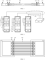
- the bidirectional terahertz cable 201 may be applied between service devices 202 and a cabinet top switch 203 in a same cabinet, may be applied between the service device 202 and the cabinet top switch 203 in another cabinet, or may be applied between the cabinet top switch 203 and a convergence switch 204.
- boards of two devices may be interconnected through a plurality of pairs of terahertz cables.
- boards 301 of devices at two communication ends are connected through a plurality of pairs of terahertz transmission lines.
- a plurality of radio frequency transceiver chips 302 are installed on the boards 301 of the devices, and each radio frequency transceiver chip 302 is coupled to the terahertz transmission line 304 through the mode conversion structure 303, to receive and transmit a terahertz signal. In this way, direct on-board high-density interconnection can be implemented between two devices.
- FIG. 4 A structure of the terahertz carrier sending apparatus provided in this embodiment of the present invention is shown in FIG. 4 , and includes a printed circuit board (PCB) 401, a radio frequency sending chip 402, a mode conversion structure 403, and a terahertz transmission line 404.
- the radio frequency sending chip 402 includes a radio frequency sending circuit 421, a feed transmission line 422, and a mode excitation structure 423.
- a terahertz signal is generated by the radio frequency sending circuit 421 and output to the mode excitation structure 423 through the feed transmission line 422.
- the mode conversion structure 403 couples the terahertz signal in the mode excitation structure 423 into the terahertz transmission line 404, and transmits the terahertz signal to a receiver.
- a baseband signal processing chip 405 is further packaged on the PCB.
- the baseband signal processing chip may not be packaged in the terahertz carrier sending apparatus, but is packaged on a service processing board of a transmitting device.
- FIG. 5 A schematic diagram of a structure of the terahertz carrier receiving apparatus according to an embodiment of the present invention is shown in FIG. 5 , and the terahertz carrier receiving apparatus includes a printed circuit board (PCB) 501, a radio frequency receiving chip 502, a mode conversion structure 503, and a terahertz transmission line 504.
- the radio frequency receiving chip 502 includes a mode excitation structure 523, a feed transmission line 522, and a radio frequency receiving circuit 521.
- the mode excitation structure 503 couples a terahertz signal received through the terahertz transmission line 504 into the mode excitation structure 523, and transmits the terahertz signal to the radio frequency receiving circuit 521 through the feed transmission line 522.
- a baseband signal processing chip 505 is further packaged on the PCB board shown in FIG. 5 . Similarly, the baseband signal processing chip may not be packaged in the terahertz carrier receiving apparatus, but is packaged on a service processing board of a receiving device.
- a terahertz carrier sending apparatus and a terahertz carrier receiving apparatus at a communication end may be combined into one transceiver apparatus.
- the radio frequency sending chip 402 and the radio frequency receiving chip 502 may be combined into one radio frequency transceiver chip, and the transceiver apparatus includes a radio frequency sending circuit and a radio frequency receiving circuit (referred to as a radio frequency transceiver circuit below), a feed transmission line, and a mode excitation structure.
- the feed transmission line and the mode excitation structure may be used for both signal transmission and signal reception.
- the mode conversion structure and the terahertz transmission line may also be used for transmission and reception. The following uses an example for description.
- FIG. 6 is a schematic diagram of a three-dimensional structure of components of a terahertz carrier transceiver apparatus according to an embodiment of the present invention
- the terahertz carrier transceiver apparatus includes a printed circuit board (PCB) 601, a radio frequency transceiver chip 602, a mode conversion structure 603, and a terahertz transmission line 604.
- PCB printed circuit board
- a radio frequency transceiver chip 602 a mode conversion structure 603
- a baseband signal processing chip 605 is further packaged on the PCB.
- FIG. 7a A schematic diagram of a three-dimensional structure of a radio frequency transceiver chip is shown in FIG. 7a , and the radio frequency transceiver chip includes a radio frequency transceiver circuit 701, a feed transmission line 702, and a mode excitation structure 703. Further, refer to FIG. 7b.
- FIG. 7b is a cross-sectional view of the radio frequency transceiver chip shown in FIG. 7a .
- a left part of the dashed line corresponds to the radio frequency transceiver circuit 701
- a right part of the dashed line corresponds to the feed transmission line 702 and the mode excitation structure 703.
- CMOS chip When the chip is manufactured, a standard CMOS chip may generally be used.
- an on-chip feed transmission line, a metal ground, and an on-chip mode excitation structure are constructed by using a top metal layer 711, a bottom metal layer 712, and a dielectric layer 714 between the top metal layer 711 and the bottom metal layer 712 together.
- a part or all of a metal distribution structure 715 between the feed transmission line and the on-chip mode excitation structure is etched off by using a standard CMOS chip processing technology, to form one or more layers of dielectric layers.
- the mode excitation structure 703 may be a linearly tapered slot antenna structure, or may be a dipole antenna structure.
- FIG. 7a shows the mode excitation structure 703 in the dipole antenna structure.
- An example of the mode excitation structure 703 in the linearly tapered slot antenna structure is described later.
- the dielectric layer between the top metal layer 711 and the bottom metal 712 may be a single layer or a plurality of layers.
- a thickness Sub_t of the dielectric layer is controlled between 1.5 to 200 times that of a larger one between the top metal layer and the bottom metal layer, that is, the following formula 1 condition is met. 1.5 ⁇ Max Top _ t , Bottom _ t ⁇ Sub _ t ⁇ 200 ⁇ Max Top _ t , Bottom _ t
- Top_t is a thickness of the top metal layer
- Bottom_t is a thickness of the bottom metal layer.
- an inner wall of the mode conversion structure 603 is metal, and an inner cavity enclosed by the metal inner wall is coupled to the mode excitation structure of the radio frequency transceiver chip.
- a to-be-sent terahertz signal is transmitted from the radio frequency sending circuit to the mode excitation structure, and the mode conversion structure 603 couples the terahertz signal in the mode excitation structure 703 into the terahertz transmission line for sending.
- the mode conversion structure 603 couples a terahertz signal received by the terahertz transmission line into the mode excitation structure 703, and then transmits the terahertz signal to the radio frequency receiving circuit for processing.
- the inner cavity enclosed by the metal inner wall of the mode conversion structure 603 may be columnar, and a cross section of the inner cavity may be a circle, a rectangle, or the like.
- An outer contour of the mode conversion structure 603 may be a cylinder, a cuboid shape, or the like, and a cross section of the mode conversion structure 603 may be a circle, a rectangle, or the like.
- a rectangular positioning slot 631 may be provided at an eccentric position of the inner cavity, and is configured to locate and fasten the PCB board 601. The PCB board 601 is inserted into the eccentric rectangular positioning slot 631, so that the on-chip mode excitation structure of the radio frequency transceiver chip 602 is located in the inner cavity of the mode conversion structure.
- a height and a depth of the rectangular slot and a position relationship between the rectangular slot and the PCB board are set, to ensure that an equivalent phase center of the on-chip mode excitation structure 703 is on a geometric central axis of the mode conversion structure 603. Therefore, high-efficiency coupling can be implemented.
- the terahertz transmission line 604 may be inserted into the mode conversion structure 603, to form a terahertz radio frequency link.
- the terahertz transmission line may be a solid core transmission line or a hollow core transmission line.
- a cross section of the terahertz transmission line may be a circle, a rectangle, or other shapes.
- a service signal enters the terahertz radio frequency link through a baseband signal processing chip at the transmitting end, and is transmitted to the receiving end. Then, the service signal is converted into a service signal through a baseband signal processing chip at the receiving end. In this way, high-speed interconnection of service signals is implemented.
- FIG. 8a is a three-dimensional schematic diagram of a packaged terahertz carrier transceiver apparatus according to an embodiment of the present invention
- the terahertz carrier transceiver apparatus includes a printed circuit board (PCB) 801, a radio frequency transceiver chip 802, a mode conversion structure 803, and a terahertz transmission line 804.
- PCB printed circuit board
- the following uses a CMOS process as an example to describe a detailed design of the terahertz carrier transceiver apparatus.
- a specific structure of the radio frequency transceiver chip 802 is shown in FIG. 8b , and the radio frequency transceiver chip 802 includes a feed transmission line 821, a tapered microstrip line 822, a substrate integrated waveguide 823, and a mode excitation structure 824.
- an M1 metal layer is bottom metal
- an M9 metal layer is top metal.
- all metal between M1 and M9 is etched away, to form a plurality of layers of equivalent dielectric layers.
- a top metal layer in the on-chip feed transmission line area is a microstrip structure of the on-chip feed transmission line
- an equivalent dielectric layer is a dielectric substrate
- a bottom metal layer is a metal ground.
- the on-chip feed transmission line 821 is connected to a radio frequency transceiver circuit.
- the radio frequency transceiver chip further has a tapered microstrip line 822, the tapered microstrip line 822 is a first segment of an impedance matching structure, and the tapered microstrip line 822 implements connection between the on-chip feed transmission line 821 and the substrate integrated waveguide 823.
- the on-chip tapered microstrip line 822 also uses a top metal layer as an on-chip microstrip structure, an equivalent dielectric layer as a dielectric substrate, and a bottom metal layer as a metal ground.
- the substrate integrated waveguide 823 on the radio frequency transceiver chip is a second segment of the impedance matching structure, and uses top layer metal and bottom layer metal in the chip respectively as upper and lower layers of metal of the substrate integrated waveguide, and an equivalent dielectric layer is used as an intermediate dielectric layer.
- the on-chip feed transmission line 821 is connected to an on-chip radiator, that is, the mode excitation structure 824, through the tapered microstrip line 822, and the substrate integrated waveguide 823.
- the on-chip mode excitation structure 824 shown in FIG. 8b uses an end-fire linearly tapered slot antenna, and has a triangular metal patch radiator on both a top metal layer and a bottom metal layer.
- the two metal patch radiators are mirror-symmetric along a y-axis direction shown in the figure by using a central axis of the equivalent dielectric layer as a center line.
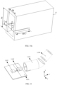
- FIG. 8c A specific structure of the mode conversion structure 803 is shown in FIG. 8c .
- An inner wall of the mode conversion structure 803 forms a cylindrical inner cavity, a material of the inner wall is metal, and an outer contour of the mode conversion structure 803 is a square cylinder.
- a rectangular positioning slot is provided in an eccentric direction of an x-axis of the mode conversion structure 803, and the PCB board is aligned with and fastened to the positioning slot, so that a part or all of the on-chip feed transmission line and the mode excitation structure on the radio frequency transceiver chip 802 can be inserted into the mode conversion structure.
- an axis of an equivalent phase center of the on-chip mode excitation structure coincides with a central axis of the cylindrical inner cavity of the metal mode conversion structure. Therefore, high-efficiency coupling can be implemented.
- One end of the terahertz transmission line 804 that is inserted into the mode conversion structure 803 has a tapered structure that can couple a terahertz signal into the transmission line.
- the other end of the solid core dielectric terahertz transmission line with a same tapered structure is inserted into the mode conversion structure, so that a terahertz signal in the transmission line can be coupled into the mode excitation structure in the radio frequency receiving chip, to form a terahertz radio frequency link. Therefore, high-speed interconnection of high-speed service signals from a transmitting end to a receiving end can be implemented.
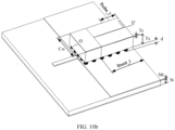
- Tc is a thickness from the top metal layer to the bottom metal layer of the radio frequency transceiver chip
- Ts is a thickness of the silicon-based substrate of the radio frequency transceiver chip
- d is a height from the silicon-based substrate of the chip to the PCB board
- S_d is an eccentric distance of the rectangular positioning slot.
- a diameter Cd of the inner cavity of the mode conversion structure 803 should be greater than or equal to a width Cw of the radio frequency transceiver chip 802.
- Slot_h is a height of the rectangular positioning slot of the mode conversion structure 803
- Mt is a thickness of a top metal layer of the PCB board
- Mt is a thickness of a bottom metal layer of the PCB board
- St is a thickness of a middle layer of the PCB board.
- Insert_1 is a depth at which the PCB board is inserted into the mode conversion structure
- Slot_l is a depth of the rectangular positioning slot of the mode conversion structure
- Probe_1 is a length of the on-chip mode excitation structure.
- a central axis OO of a dielectric substrate of the on-chip mode excitation structure 824 should coincide with a central axis QQ of the mode conversion structure 803, that is, the two central axes need to coincide and need to be less than a set error range during installation.
- simulation is performed by using a 65 nm silicon-based CMOS chip process as an example.
- the terahertz transmission line is a solid core wire with a round section, a diameter of 1.65 mm and a material of polytetrafluoroethylene.
- the circular cross-sectional diameter of the cylindrical inner cavity of the mode conversion structure is set to be 1.65 mm, which is the same as the diameter of the terahertz transmission line.
- a width Cw of the radio frequency transceiver chip is 1.40 mm
- a metal thickness of the M9 layer is 3.40 ⁇ m
- a metal thickness of the M1 layer is 0.77 ⁇ m
- a thickness of the equivalent dielectric layer is 10.28 ⁇ m
- a length Probe_1 of an excitation probe is 0.80 mm
- a length Insert_1 for the chip to enter the mode conversion structure is 2.00 mm.
- FIG. 9a a schematic diagram of electric field mode distribution shown in FIG. 9a may be obtained through electromagnetic simulation calculation.
- An electromagnetic signal is connected from the radio frequency sending circuit to the on-chip substrate integrated waveguide 823 through the on-chip feed microstrip line 821, to convert from a quasi-transverse electro-magnetic (Transverse Electro-Magnetic, TEM) mode to a quasi-transverse electro 10 (Transverse Electro, TE 10 ) mode.
- TEM Transverse Electro-Magnetic
- TE 10 quasi-transverse electro 10
- the electromagnetic signal is transmitted to the linearly tapered slot mode excitation structure 824, to excite a transmission fundamental mode transverse electro 11 (Transverse Electro, TE 11 ) mode in the circular metal mode conversion structure, and an electromagnetic wave is coupled, through the mode conversion structure 803, into the solid core terahertz transmission line 804 with a tapered end face, to implement fundamental mode transmission in a hybrid electro 11 (Hybrid Electro, HE 11 ) mode.
- a transmission parameter from the radio frequency sending circuit to the terahertz transmission line is greater than -4 dB. This indicates that coupling efficiency from the radio frequency sending circuit to the terahertz transmission line is very high. Therefore, a link interconnection length can be significantly increased by using such a terahertz transceiver.
- FIG. 9b a schematic diagram of spatial electric field distribution shown in FIG. 9b may also be obtained through electromagnetic simulation calculation. From FIG. 9b , it can be learned that an electromagnetic signal is fed from the on-chip microstrip line 821, enters the mode excitation structure 824 through the substrate integrated waveguide 823, and is coupled into the solid core terahertz transmission line 804 through the mode conversion structure 803. There is almost no electromagnetic energy leakage in space. This indicates that this embodiment of the present invention has good electromagnetic shielding performance, excellent anti-electromagnetic interference capability, and further improves transmission bandwidth.
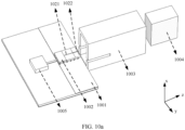
- An embodiment of the present invention further provides a terahertz transceiver apparatus, as shown in FIG. 10a .
- a mode excitation structure 1022 on a radio frequency transceiver chip 1002 uses a dipole antenna, and feeds the dipole antenna through an on-chip microstrip line 1021, and the on-chip dipole antenna has an L-shaped metal patch radiator on both a top metal layer and a bottom metal layer.
- the two metal radiators are mirror-symmetric along a y-axis direction as shown in the figure, and use an axis of an equivalent dielectric layer as a center line.
- a cross section of an inner cavity of a mode conversion structure 1003 is rectangular, a material of an inner wall of the mode conversion structure 1003 is metal, and a cross section of an outer contour of the mode conversion structure 1003 is also rectangular.
- a terahertz transmission line 1004 has a rectangular cross section, a cross section dimension of the terahertz transmission line 1004 is the same as an inner wall dimension of a cross section of the mode conversion structure, and the terahertz transmission line 1004 may be inserted into the mode conversion structure 1003.
- the mode conversion structure 1003 is provided with a rectangular positioning slot in an x-axis eccentric direction, and all the feed part and the mode excitation part on the radio frequency transceiver chip 1002 may be inserted into the mode conversion structure 1003.
- the PCB board 1001 is aligned with and fastened to and the rectangular positioning slot, so that it can be ensured that an axis on which an equivalent phase center in the on-chip mode excitation structure is located coincides with a central axis of the metal mode conversion structure. Therefore, high-efficiency coupling can be implemented.
- the conditions that related dimensions need to meet include the following formulas 5, 6, and 7.
- Tc is a thickness from the top metal layer to the bottom metal layer of the radio frequency transceiver chip
- Ts is a thickness of the silicon-based substrate of the radio frequency transceiver chip
- d is a height from the silicon-based substrate of the chip to the PCB board
- S_d is an eccentric distance of the rectangular positioning slot.
- a length Rb of the inner cavity of the mode conversion structure 1003 along the y-axis direction should be greater than or equal to a width Cw of the radio frequency transceiver chip 1002.
- Slot_h is a height of the rectangular positioning slot of the mode conversion structure 1003
- Mt is a thickness of a top metal layer of the PCB board
- Mt is a thickness of a bottom metal layer of the PCB board
- St is a thickness of a middle layer of the PCB board.
- Insert_1 is a depth at which the PCB board is inserted into the mode conversion structure
- Slot_1 is a depth of the rectangular positioning slot of the mode conversion structure
- Probe_1 is a length of the on-chip mode excitation structure.
- a central axis OO of a dielectric substrate of the on-chip mode excitation structure 1022 should coincide with a central axis QQ of the mode conversion structure 1003, that is, the two central axes need to coincide and need to be less than a set error range during installation.
- An embodiment of the present invention further provides a terahertz transceiver apparatus, as shown in FIG. 11 .
- a mode conversion structure 1103 uses a curved end face structure, so that non-parallel coupling between a terahertz transmission line and a radio frequency transceiver chip can be implemented, and adaptation of the terahertz transceiver apparatus can be improved.
Landscapes
- Engineering & Computer Science (AREA)
- Computer Networks & Wireless Communication (AREA)
- Signal Processing (AREA)
- Waveguide Aerials (AREA)
- Transceivers (AREA)
Applications Claiming Priority (2)
| Application Number | Priority Date | Filing Date | Title |
|---|---|---|---|
| CN202011636176.8A CN114696874A (zh) | 2020-12-31 | 2020-12-31 | 太赫兹载波发送装置和接收装置 |
| PCT/CN2021/140075 WO2022143299A1 (fr) | 2020-12-31 | 2021-12-21 | Dispositif d'émission de porteuse terahertz et dispositif de réception de porteuse terahertz |
Publications (2)
| Publication Number | Publication Date |
|---|---|
| EP4262096A1 true EP4262096A1 (fr) | 2023-10-18 |
| EP4262096A4 EP4262096A4 (fr) | 2024-06-26 |
Family
ID=82133389
Family Applications (1)
| Application Number | Title | Priority Date | Filing Date |
|---|---|---|---|
| EP21914038.1A Pending EP4262096A4 (fr) | 2020-12-31 | 2021-12-21 | Dispositif d'émission de porteuse terahertz et dispositif de réception de porteuse terahertz |
Country Status (4)
| Country | Link |
|---|---|
| US (1) | US12476382B2 (fr) |
| EP (1) | EP4262096A4 (fr) |
| CN (1) | CN114696874A (fr) |
| WO (1) | WO2022143299A1 (fr) |
Families Citing this family (1)
| Publication number | Priority date | Publication date | Assignee | Title |
|---|---|---|---|---|
| FR3090109B1 (fr) * | 2018-12-14 | 2024-06-28 | Univ Paris Sud | Capteur micro-onde du type à micro-ruban |
Family Cites Families (14)
| Publication number | Priority date | Publication date | Assignee | Title |
|---|---|---|---|---|
| US6967347B2 (en) * | 2001-05-21 | 2005-11-22 | The Regents Of The University Of Colorado | Terahertz interconnect system and applications |
| JP4127087B2 (ja) * | 2003-03-20 | 2008-07-30 | 旭硝子株式会社 | アンテナ装置および無線装置 |
| US9191263B2 (en) * | 2008-12-23 | 2015-11-17 | Keyssa, Inc. | Contactless replacement for cabled standards-based interfaces |
| CN101794953A (zh) * | 2010-02-01 | 2010-08-04 | 湖南大学 | 基于光学四波混频效应的太赫兹波产生装置及方法 |
| CN103119714B (zh) | 2010-09-21 | 2016-08-17 | 德克萨斯仪器股份有限公司 | 利用亚毫米波和介电波导的芯片到芯片通信 |
| WO2014171292A1 (fr) * | 2013-04-18 | 2014-10-23 | ソニー株式会社 | Dispositif de connecteur et système de transmission sans fil |
| US9461706B1 (en) * | 2015-07-31 | 2016-10-04 | At&T Intellectual Property I, Lp | Method and apparatus for exchanging communication signals |
| DE112015005575T5 (de) * | 2014-12-12 | 2017-09-28 | Sony Corporation | Mikrowellenantennenvorrichtung, einheit und herstellungsverfahren |
| US10587223B2 (en) * | 2015-02-20 | 2020-03-10 | Cornell University | Device for terahertz signal generation and transmitter |
| CN109473757B (zh) * | 2015-07-30 | 2020-03-10 | 上海理工大学 | 一种宽频传输线芯片 |
| US9490518B1 (en) | 2015-09-28 | 2016-11-08 | Texas Instruments Incorporated | System for launching a signal into a dielectric waveguide |
| US10581141B2 (en) * | 2016-10-21 | 2020-03-03 | DISH Technologies L.L.C. | RF antenna arrangement configured to be a part of a lid to an apparatus |
| KR102456844B1 (ko) * | 2018-11-27 | 2022-10-21 | 한국전자통신연구원 | 초고주파 기반 빔포밍 안테나 및 이를 이용한 통신 방법 |
| CN114204247B (zh) * | 2020-09-16 | 2025-09-05 | 华为技术有限公司 | 射频芯片、信号收发机和通信设备 |
-
2020
- 2020-12-31 CN CN202011636176.8A patent/CN114696874A/zh active Pending
-
2021
- 2021-12-21 EP EP21914038.1A patent/EP4262096A4/fr active Pending
- 2021-12-21 WO PCT/CN2021/140075 patent/WO2022143299A1/fr not_active Ceased
-
2023
- 2023-06-29 US US18/216,433 patent/US12476382B2/en active Active
Also Published As
| Publication number | Publication date |
|---|---|
| EP4262096A4 (fr) | 2024-06-26 |
| CN114696874A (zh) | 2022-07-01 |
| US12476382B2 (en) | 2025-11-18 |
| WO2022143299A1 (fr) | 2022-07-07 |
| US20230344145A1 (en) | 2023-10-26 |
Similar Documents
| Publication | Publication Date | Title |
|---|---|---|
| KR102614892B1 (ko) | 안테나 유닛 및 단말 장비 | |
| KR101605218B1 (ko) | 밀리미터파 유전체 내 전송 장치 및 그 제조 방법, 및 무선 전송 장치 및 무선 전송 방법 | |
| JP7313479B2 (ja) | アンテナユニット及び端末機器 | |
| EP2988365B1 (fr) | Dispositif de connecteur et système de transmission sans fil | |
| JP4995174B2 (ja) | 無線通信装置 | |
| EP2652879B1 (fr) | Directeurs de champ proche périodique (pnfd) pour interconnexion sans fil en ondes millimétriques (interconnexion m2w2) à courte portée | |
| EP3890107B1 (fr) | Antenne bande à ultra large et terminal de communication | |
| US20230352807A1 (en) | Terahertz Carrier Sending Apparatus and Terahertz Carrier Receiving Apparatus | |
| EP3849015A1 (fr) | Antenne et terminal mobile | |
| US12476382B2 (en) | Terahertz carrier sending apparatus and terahertz carrier receiving apparatus | |
| CN202444055U (zh) | 微带阵列天线 | |
| US20240372237A1 (en) | Transformative apparatus, arrayed transformative apparatus, and communication device | |
| TWI539668B (zh) | Antenna device and communication device | |
| KR101001664B1 (ko) | 수직 편파 및 수평 편파의 동시 송수신이 가능한 안테나 | |
| CN116601828B (zh) | 基站天线 | |
| CN116014400A (zh) | 一种矩形波导、喇叭天线及片上系统 | |
| US10938089B2 (en) | Millimeter wave communication through device case | |
| CN115441167A (zh) | 集成有双工器的紧凑型低剖面开孔天线 | |
| CN214589253U (zh) | 一种背馈单孔双馈微带天线 | |
| EP4518030A1 (fr) | Module d'antenne et dispositif de communication | |
| US20250141111A1 (en) | Antenna array and ground station | |
| CN120709724A (zh) | 毫米波天线和通信设备 | |
| CN120581858A (zh) | 天线及电子设备 | |
| JP5727177B2 (ja) | アンテナ装置、及び、通信装置 | |
| CN107681269A (zh) | 射频电流抑制结构及射频收发系统 |
Legal Events
| Date | Code | Title | Description |
|---|---|---|---|
| STAA | Information on the status of an ep patent application or granted ep patent |
Free format text: STATUS: THE INTERNATIONAL PUBLICATION HAS BEEN MADE |
|
| PUAI | Public reference made under article 153(3) epc to a published international application that has entered the european phase |
Free format text: ORIGINAL CODE: 0009012 |
|
| STAA | Information on the status of an ep patent application or granted ep patent |
Free format text: STATUS: REQUEST FOR EXAMINATION WAS MADE |
|
| 17P | Request for examination filed |
Effective date: 20230712 |
|
| AK | Designated contracting states |
Kind code of ref document: A1 Designated state(s): AL AT BE BG CH CY CZ DE DK EE ES FI FR GB GR HR HU IE IS IT LI LT LU LV MC MK MT NL NO PL PT RO RS SE SI SK SM TR |
|
| DAV | Request for validation of the european patent (deleted) | ||
| DAX | Request for extension of the european patent (deleted) | ||
| REG | Reference to a national code |
Ref country code: DE Ref legal event code: R079 Free format text: PREVIOUS MAIN CLASS: H04B0005000000 Ipc: H01P0005080000 |
|
| A4 | Supplementary search report drawn up and despatched |
Effective date: 20240524 |
|
| RIC1 | Information provided on ipc code assigned before grant |
Ipc: H01Q 13/08 20060101ALN20240517BHEP Ipc: H01Q 9/28 20060101ALN20240517BHEP Ipc: H04B 3/04 20060101ALI20240517BHEP Ipc: H01P 5/08 20060101AFI20240517BHEP |