EP4264669B1 - Multispektraler infrarot-fotodetektor - Google Patents
Multispektraler infrarot-fotodetektor Download PDFInfo
- Publication number
- EP4264669B1 EP4264669B1 EP21851681.3A EP21851681A EP4264669B1 EP 4264669 B1 EP4264669 B1 EP 4264669B1 EP 21851681 A EP21851681 A EP 21851681A EP 4264669 B1 EP4264669 B1 EP 4264669B1
- Authority
- EP
- European Patent Office
- Prior art keywords
- filtering
- stage
- matrix
- wavelengths
- spectral band
- Prior art date
- Legal status (The legal status is an assumption and is not a legal conclusion. Google has not performed a legal analysis and makes no representation as to the accuracy of the status listed.)
- Active
Links
Images


Classifications
-
- H—ELECTRICITY
- H10—SEMICONDUCTOR DEVICES; ELECTRIC SOLID-STATE DEVICES NOT OTHERWISE PROVIDED FOR
- H10F—INORGANIC SEMICONDUCTOR DEVICES SENSITIVE TO INFRARED RADIATION, LIGHT, ELECTROMAGNETIC RADIATION OF SHORTER WAVELENGTH OR CORPUSCULAR RADIATION
- H10F39/00—Integrated devices, or assemblies of multiple devices, comprising at least one element covered by group H10F30/00, e.g. radiation detectors comprising photodiode arrays
- H10F39/80—Constructional details of image sensors
- H10F39/805—Coatings
-
- H—ELECTRICITY
- H10—SEMICONDUCTOR DEVICES; ELECTRIC SOLID-STATE DEVICES NOT OTHERWISE PROVIDED FOR
- H10F—INORGANIC SEMICONDUCTOR DEVICES SENSITIVE TO INFRARED RADIATION, LIGHT, ELECTROMAGNETIC RADIATION OF SHORTER WAVELENGTH OR CORPUSCULAR RADIATION
- H10F39/00—Integrated devices, or assemblies of multiple devices, comprising at least one element covered by group H10F30/00, e.g. radiation detectors comprising photodiode arrays
- H10F39/011—Manufacture or treatment of image sensors covered by group H10F39/12
- H10F39/021—Manufacture or treatment of image sensors covered by group H10F39/12 of image sensors having active layers comprising only Group III-V materials, e.g. GaAs, AlGaAs or InP
-
- H—ELECTRICITY
- H10—SEMICONDUCTOR DEVICES; ELECTRIC SOLID-STATE DEVICES NOT OTHERWISE PROVIDED FOR
- H10F—INORGANIC SEMICONDUCTOR DEVICES SENSITIVE TO INFRARED RADIATION, LIGHT, ELECTROMAGNETIC RADIATION OF SHORTER WAVELENGTH OR CORPUSCULAR RADIATION
- H10F39/00—Integrated devices, or assemblies of multiple devices, comprising at least one element covered by group H10F30/00, e.g. radiation detectors comprising photodiode arrays
- H10F39/011—Manufacture or treatment of image sensors covered by group H10F39/12
- H10F39/024—Manufacture or treatment of image sensors covered by group H10F39/12 of coatings or optical elements
-
- H—ELECTRICITY
- H10—SEMICONDUCTOR DEVICES; ELECTRIC SOLID-STATE DEVICES NOT OTHERWISE PROVIDED FOR
- H10F—INORGANIC SEMICONDUCTOR DEVICES SENSITIVE TO INFRARED RADIATION, LIGHT, ELECTROMAGNETIC RADIATION OF SHORTER WAVELENGTH OR CORPUSCULAR RADIATION
- H10F39/00—Integrated devices, or assemblies of multiple devices, comprising at least one element covered by group H10F30/00, e.g. radiation detectors comprising photodiode arrays
- H10F39/10—Integrated devices
- H10F39/12—Image sensors
- H10F39/18—Complementary metal-oxide-semiconductor [CMOS] image sensors; Photodiode array image sensors
- H10F39/184—Infrared image sensors
- H10F39/1843—Infrared image sensors of the hybrid type
-
- H—ELECTRICITY
- H10—SEMICONDUCTOR DEVICES; ELECTRIC SOLID-STATE DEVICES NOT OTHERWISE PROVIDED FOR
- H10F—INORGANIC SEMICONDUCTOR DEVICES SENSITIVE TO INFRARED RADIATION, LIGHT, ELECTROMAGNETIC RADIATION OF SHORTER WAVELENGTH OR CORPUSCULAR RADIATION
- H10F39/00—Integrated devices, or assemblies of multiple devices, comprising at least one element covered by group H10F30/00, e.g. radiation detectors comprising photodiode arrays
- H10F39/10—Integrated devices
- H10F39/12—Image sensors
- H10F39/191—Photoconductor image sensors
- H10F39/193—Infrared image sensors
- H10F39/1935—Infrared image sensors of the hybrid type
-
- H—ELECTRICITY
- H10—SEMICONDUCTOR DEVICES; ELECTRIC SOLID-STATE DEVICES NOT OTHERWISE PROVIDED FOR
- H10F—INORGANIC SEMICONDUCTOR DEVICES SENSITIVE TO INFRARED RADIATION, LIGHT, ELECTROMAGNETIC RADIATION OF SHORTER WAVELENGTH OR CORPUSCULAR RADIATION
- H10F39/00—Integrated devices, or assemblies of multiple devices, comprising at least one element covered by group H10F30/00, e.g. radiation detectors comprising photodiode arrays
- H10F39/80—Constructional details of image sensors
- H10F39/806—Optical elements or arrangements associated with the image sensors
-
- H—ELECTRICITY
- H10—SEMICONDUCTOR DEVICES; ELECTRIC SOLID-STATE DEVICES NOT OTHERWISE PROVIDED FOR
- H10F—INORGANIC SEMICONDUCTOR DEVICES SENSITIVE TO INFRARED RADIATION, LIGHT, ELECTROMAGNETIC RADIATION OF SHORTER WAVELENGTH OR CORPUSCULAR RADIATION
- H10F39/00—Integrated devices, or assemblies of multiple devices, comprising at least one element covered by group H10F30/00, e.g. radiation detectors comprising photodiode arrays
- H10F39/80—Constructional details of image sensors
- H10F39/806—Optical elements or arrangements associated with the image sensors
- H10F39/8063—Microlenses
-
- H—ELECTRICITY
- H10—SEMICONDUCTOR DEVICES; ELECTRIC SOLID-STATE DEVICES NOT OTHERWISE PROVIDED FOR
- H10F—INORGANIC SEMICONDUCTOR DEVICES SENSITIVE TO INFRARED RADIATION, LIGHT, ELECTROMAGNETIC RADIATION OF SHORTER WAVELENGTH OR CORPUSCULAR RADIATION
- H10F39/00—Integrated devices, or assemblies of multiple devices, comprising at least one element covered by group H10F30/00, e.g. radiation detectors comprising photodiode arrays
- H10F39/80—Constructional details of image sensors
- H10F39/806—Optical elements or arrangements associated with the image sensors
- H10F39/8067—Reflectors
-
- H—ELECTRICITY
- H10—SEMICONDUCTOR DEVICES; ELECTRIC SOLID-STATE DEVICES NOT OTHERWISE PROVIDED FOR
- H10F—INORGANIC SEMICONDUCTOR DEVICES SENSITIVE TO INFRARED RADIATION, LIGHT, ELECTROMAGNETIC RADIATION OF SHORTER WAVELENGTH OR CORPUSCULAR RADIATION
- H10F39/00—Integrated devices, or assemblies of multiple devices, comprising at least one element covered by group H10F30/00, e.g. radiation detectors comprising photodiode arrays
- H10F39/10—Integrated devices
- H10F39/12—Image sensors
- H10F39/199—Back-illuminated image sensors
-
- H—ELECTRICITY
- H10—SEMICONDUCTOR DEVICES; ELECTRIC SOLID-STATE DEVICES NOT OTHERWISE PROVIDED FOR
- H10F—INORGANIC SEMICONDUCTOR DEVICES SENSITIVE TO INFRARED RADIATION, LIGHT, ELECTROMAGNETIC RADIATION OF SHORTER WAVELENGTH OR CORPUSCULAR RADIATION
- H10F39/00—Integrated devices, or assemblies of multiple devices, comprising at least one element covered by group H10F30/00, e.g. radiation detectors comprising photodiode arrays
- H10F39/80—Constructional details of image sensors
- H10F39/811—Interconnections
-
- H—ELECTRICITY
- H10—SEMICONDUCTOR DEVICES; ELECTRIC SOLID-STATE DEVICES NOT OTHERWISE PROVIDED FOR
- H10W—GENERIC PACKAGES, INTERCONNECTIONS, CONNECTORS OR OTHER CONSTRUCTIONAL DETAILS OF DEVICES COVERED BY CLASS H10
- H10W72/00—Interconnections or connectors in packages
- H10W72/20—Bump connectors, e.g. solder bumps or copper pillars; Dummy bumps; Thermal bumps
- H10W72/251—Materials
- H10W72/252—Materials comprising solid metals or solid metalloids, e.g. PbSn, Ag or Cu
-
- H—ELECTRICITY
- H10—SEMICONDUCTOR DEVICES; ELECTRIC SOLID-STATE DEVICES NOT OTHERWISE PROVIDED FOR
- H10W—GENERIC PACKAGES, INTERCONNECTIONS, CONNECTORS OR OTHER CONSTRUCTIONAL DETAILS OF DEVICES COVERED BY CLASS H10
- H10W90/00—Package configurations
- H10W90/701—Package configurations characterised by the relative positions of pads or connectors relative to package parts
- H10W90/721—Package configurations characterised by the relative positions of pads or connectors relative to package parts of bump connectors
- H10W90/722—Package configurations characterised by the relative positions of pads or connectors relative to package parts of bump connectors between stacked chips
Definitions
- the invention relates to a multispectral infrared photodetection device, i.e. a photon detection device, sensitive in the infrared, and comprising at least two types of pixels which differ by their respective spectral sensitivity ranges.
- a multispectral infrared photodetection device i.e. a photon detection device, sensitive in the infrared, and comprising at least two types of pixels which differ by their respective spectral sensitivity ranges.
- a multispectral infrared photodetection device i.e. a photon detection device, sensitive in the infrared, and comprising at least two types of pixels which differ by their respective spectral sensitivity ranges.
- a device is coupled to a cooler, to lower its temperature to cryogenic temperatures.
- a multispectral infrared photodetection device conventionally comprises a matrix of photodiodes integrated in a semiconductor substrate, and spectral filters to filter the infrared light arriving on the photodiodes.
- the semiconductor substrate here called active layer, advantageously rests on a support substrate (growth substrate after thinning) which gives the assembly the desired mechanical rigidity.
- the invention relates more particularly to a so-called “hybridized” photodetection device, i.e. incorporating a photodiode reading circuit which is located under the photodiode matrix.
- the reading circuit is electrically connected to each of the photodiodes of the photodiode matrix, generally by metal balls.
- An objective of the present invention is to propose a hybridized multi-spectral infrared photo-detection device offering improved performance in terms of color reconstruction, in comparison with the prior art.
- the support substrate may correspond to the residual part of an active layer growth substrate, after thinning.
- An interference filter is a filter in which the separation of wavelengths is based on the transmission of light in one wavelength range and the reflection of light in another wavelength range (as opposed to absorbent filters consisting, for example, of a colored resin in the visible range).
- the photodetection stage including the photodiode array and its readout circuit, forms a hybrid component.
- the active layer is formed on a growth substrate, then hybridized with it on the reading circuit. Then, the growth substrate is thinned, to form the support substrate.
- This method makes it possible to have the flattest possible surface at the support substrate, on the side opposite the active layer.
- the planarization cannot be perfect.
- the hybridized component is brought to very low temperatures, which exacerbates the residual flatness defect (due in particular to the difference in thermal expansion coefficient between the material of the reading circuit and the material of the active layer).
- the filtering stage is preferably made separately and then attached by gluing to the photodetection stage.
- This layer of glue advantageously has a thickness that varies in space, to compensate for the lack of flatness of the support substrate.
- pixels are defined, each comprising a single photodiode of the photodiode matrix.
- it is necessary to bring the filtering stage and the photodiode matrix as close as possible. It is also necessary to maintain a certain thickness of the support substrate, to guarantee good mechanical stability of the device according to the invention.
- the bringing together of the filtering stage and the photodiode matrix then involves a layer of glue that is as thin as possible.
- the inventors then made the following observation: when the adhesive layer is in direct physical contact with the support substrate, an interface between the adhesive layer and the support substrate forms a reflective surface at infrared wavelengths, in particular at the wavelengths detected by the photodiode array.
- the filtering zones of the filtering zone array are also capable of reflecting light inside the photodetection device, in particular the filtering zones each formed by an interference filter.
- An optical cavity is thus formed, above the photodetection stage, between the support substrate and the interference filters of the filtering zone matrix. In each pixel of the photodetection device, the optical cavity is excited locally, at the wavelengths transmitted by the interference filter belonging to said pixel (the filter is not perfect, and reflects a little at these wavelengths).
- the optical cavity is excited by light transmitted through the filtering zone belonging to said pixel.
- the optical cavity is also excited by light blocked by the filtering zone of a neighboring pixel, and reaching the pixel in question due, for example, to diffraction phenomena. This light, blocked by the neighboring pixel, is largely reflected by the interference filter forming the filtering zone of the pixel in question.
- the reflective surface formed at the interface between the adhesive layer and the support substrate, has a non-planar topology, with hollows and/or bumps.
- the optical cavity therefore has a variable thickness, which depends on the location considered in a plane parallel to the plane of the photodiode matrix (the thickness of the optical cavity being defined along an axis orthogonal to the plane of the filtering zone matrix).
- the photodetection device is brought to very low temperatures, which exacerbates the variations in thickness of the optical cavity, due to the difference in thermal expansion coefficient between the material of the active layer and the material(s) of the filtering zone matrix.
- the thinner the glue layer the more sensitive this cavity is to variations in its thickness.
- This greater sensitivity of the optical cavity to variations in its thickness results in greater disparities in the rate of light reaching the photodiodes from one pixel to another, and therefore in a greater disparity in a quantum efficiency coefficient from one pixel to another.
- the variation in thickness of the cavity affects the quantum efficiency coefficients differently, depending on whether the pixel in question has a filtering zone of the first type or a filtering zone of the second type. (especially because a coefficient of thermal expansion of the filtering zone depends on the type of said filtering zone).
- the skilled person seeks to produce a device that has both low crosstalk (between the pixels comprising a filtering zone of the first type and the pixels comprising a filtering zone of the second type), and high homogeneity of a quantum efficiency coefficient (over all the pixels of said device).
- low crosstalk is provided by the thinnest possible glue layer
- high homogeneity of the quantum efficiency coefficient is provided by a thick glue layer (to limit the sensitivity of the optical cavity to variations in its thickness).
- the inventors had the idea of finding a solution to this problem using an antireflective coating, between the glue layer and the support substrate, configured to limit parasitic reflections in the infrared which would otherwise be formed at the interface between the glue layer and the support substrate. It is thus possible to obtain a photo-detection device which has both low crosstalk (between the pixels comprising a filtering zone of the first type and the pixels comprising a filtering zone of the second type, in particular), thanks to a reduced thickness of the glue layer, and a quantum efficiency which is substantially homogeneous from one pixel to another. This improves a color reconstruction, in comparison with the prior art.
- the antireflection coating arranged between the support substrate and the adhesive layer, in direct physical contact with the adhesive layer, has in this configuration a reflection rate which is preferably strictly less than 1%, and even strictly less than 0.5% or even less than 0.1%, at the wavelengths detected by the photodiodes of the wavelength matrix and transmitted by at least one of the filtering zones.
- the characteristics of the antireflection coating are adapted to obtain such a reflection rate, taking into account the refractive index of the adhesive layer at the wavelengths considered (for example between 1.5 and 1.6 at the wavelengths considered).
- Such a reflection rate is obtained, for example by optimizing a thickness of the anti-reflective coating.
- the anti-reflective coating consists of a layer of ZnS, of a thickness adapted to have such a reflection rate when it is covered by the glue layer.
- a surface topology of the support substrate has a peak-valley amplitude greater than or equal to 3 ⁇ m at 300 K, on the glue layer side
- a surface topology of the filter stage has a surface topology with a peak-valley amplitude less than or equal to 300 nm at 300 K, on the glue layer side, a difference between these two surface topologies being compensated by variations in thickness of the glue layer.
- the device according to the invention may further comprise a matrix of microlenses, which extends between the glue layer and the filtering stage.
- a pitch of the microlenses of the microlens array may be a multiple of a pitch of the photodiodes of the photodiode array.
- the device according to the invention further comprises metal walls, which extend into the filtering layer, between neighboring filtering zones.
- At least part of at least one of the metal walls is framed by two intermediate partitions made of dielectric material.
- a thickness of the intermediate partitions, defined in a plane orthogonal to the optical axis, is advantageously between 500 nm and 50 nm.
- each filtering zone of the first type is constituted by a stack of layers each made of dielectric material.
- Each filtering zone of the second type may be capable of transmitting the wavelengths of the second spectral band and the wavelengths of the first spectral band, and made of a dielectric material called a filling material.
- each filtering zone of the second type may be capable of transmitting the wavelengths of the second spectral band and of blocking the wavelengths of the second spectral band, and constituted by a respective interference filter.
- the active layer can be made of an alloy of cadmium, mercury and tellurium.
- the figures show the axes of an orthonormal reference frame (Oxyz).
- the axis (Oz) defines a vertical axis, while the plane (Oxy) defines a horizontal plane.
- infrared refers to a portion of the light spectrum falling within a spectral band ranging from 0.78 ⁇ m to 50 ⁇ m, more preferably from 3 ⁇ m to 8 ⁇ m (mid-infrared, or LWIR) and/or from 8 ⁇ m to 15 ⁇ m (far-infrared, or LWIR).
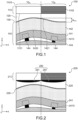
- FIG. 1 schematically illustrates, according to a sectional view in a vertical plane (Oxz), a photo-detection device 100 according to a first embodiment of the invention.
- the photo-detection device 100 is coupled to a cryogenic cooler type cooler, to lower its temperature to ultra-low temperatures, called cryogenic, in particular temperatures less than or equal to 200 K, and even less than or equal to 150 K, or even less than or equal to 120 K.
- cryogenic in particular temperatures less than or equal to 200 K, and even less than or equal to 150 K, or even less than or equal to 120 K.
- the photo-detection device 100 comprises, superimposed in this order along the axis (Oz): a filtering stage 110, a glue layer 120, an anti-reflective coating 130, and a photo-detection stage 140.
- the photodetection stage 140 comprises a semiconductor substrate 141, called the active layer, a support substrate 142, and a readout circuit 143, superimposed together along the optical axis (Oz) with the active layer 141 between the support substrate 142 and the readout circuit 143.
- a matrix of photodiodes is integrated in the active layer 141.
- the photodiodes 1401 of said matrix are schematically represented by dotted lines.
- the photodiodes 1410 are distributed in space according to a matrix arrangement, for example according to rows and columns.
- Each photodiode 1410 here defines a respective pixel of the matrix of photodiodes, as well as a respective pixel 10 A or 10 B of the photodetection device 100.
- each pixel of the photodetection device 100 is delimited by vertical surfaces extending over the entire height of the device 100, and incorporates a single photodiode 1410.
- On the figure 1 we identified the border between pixels 10 A and 10 B with a mixed line.
- the active layer 141 is here made of an alloy of cadmium, mercury and tellurium (HgCdTe).
- the invention is not limited to this material, the active layer 141 can also be made of a semiconductor alloy in III-V material such as gallium arsenide, indium arsenide, gallium nitride, gallium antimonide, or a ternary alloy such as InxGa1-xAs, etc.
- III-V material designates a material composed of one or more elements from column III of Mendeleev's periodic table (for example boron, gallium, aluminum, indium, etc.) and from column V of the same table (for example arsenic, antimony, phosphorus, etc.).
- the support substrate 142 may correspond to the residual part of a growth substrate of the active layer 141, after thinning of the latter.
- the support substrate 142 makes it possible to provide sufficient mechanical rigidity to the device 100, in particular when used at low temperature.
- the thickness of the support substrate 142, measured along the axis (Oz), is preferably greater than or equal to 10 ⁇ m, for example between 10 ⁇ m and 20 ⁇ m.
- the support substrate 142 is advantageously made of an alloy of zinc, mercury and tellurium (HgZnTe).
- the reading circuit 143 is configured to receive photocurrents generated at the photodiodes 142, and convert them into physical quantities of current type. electrical, electrical voltage, or electrical charge, compatible with signal processing chains.
- the reading circuit 143 is electrically connected to the photodiodes 1410, here by a series of indium balls 144 which each extend between one photodiode 1410 of the active layer 141 and the reading circuit 143.
- the photo-detection stage 140 thus forms a so-called “hybridized” component, incorporating both a detection circuit (the active layer 141 comprising the photodiodes) and a photodiode reading circuit (the reading circuit 143).
- the active layer 141 has in practice a certain defect in flatness.
- the largest faces of the active layer 141 instead of extending in planes parallel to the plane (Oxy), in fact have a non-flat shape with at least one hollow and/or at least one bump.
- the photo-detection device 100 is brought to a very low temperature, which exacerbates the defect in flatness, due to the difference in thermal expansion coefficient between the material of the reading circuit 143 and the material of the active layer 141.
- the active layer 141 is formed on a growth substrate, then hybridized with the reading substrate, then the growth substrate is thinned in order to obtain the support substrate 142.
- the support substrate 142 extends adjacent to the active layer 141, and has a substantially constant thickness. The thinning achieves a certain planarization of the photo-detection device 100. This planarization is however only partial, so that the planarity defect of the active layer 141 is found at least in part at the support substrate 142.
- the upper face 1421 of the support substrate 142 located on the side opposite the active layer 141, has a surface topology with at least one hollow and/or at least one bump.
- a surface topology of the upper face 1421 of the support substrate 142 has for example a peak-valley amplitude A PV greater than or equal to 3 ⁇ m at 300 K, for example between 4 ⁇ m and 5 ⁇ m at 300 K.
- This peak-valley amplitude A PV is generally reached over a distance of at least twenty pixels from the device 100. This amplitude is increased when the device 100 is brought to cryogenic temperatures, in use.
- the adhesive layer 120 extends above the upper face 1421 of the support substrate 142.
- the adhesive layer 120 makes it possible to secure the filtering stage 110 to the photo-detection stage 140, and extends more particularly between the filtering stage 110 and the support substrate 142. It is preferably made of a polymer adhesive.
- the adhesive layer 120 matches the shape of the upper face 1421 of the support substrate 142, which has a large peak-valley amplitude.
- the adhesive layer 120 matches the shape of a lower face 1101 of the filtering stage 110, which on the contrary has a substantially planar topology, close to a plane parallel to the plane (Oxy).
- a surface topology of the lower face 1101 of the filtering stage 110 has, for example, a peak-valley amplitude less than or equal to 300 nm at 300 K, and even less than or equal to 100 nm or even less than or equal to 50 nm at 300 K.
- the flatness defect brought about by the hybridization, and exacerbated by the cold setting, is therefore compensated by variations in the thickness of the glue layer 120.
- the glue layer 120 therefore allows the filtering stage 110 to have a substantially planar topology, despite the flatness defect of the photo-detection stage 140 located below.
- the average thickness of the glue layer is advantageously the smallest thickness of glue allowing compensation of at least 90% of the flatness defect, in peak-valley amplitude value. This makes it possible to bring the filtering stage 110 and the photodiode array 1410 as close as possible, and thus to limit crosstalk in the device 100.
- Crosstalk refers to the detection of a signal, by a photodiode of a pixel, generated by light incident on a neighboring pixel.
- Another way of bringing the filtering stage 110 and the photodiode array 1410 closer together may consist in reducing the thickness of the support substrate 142.
- This solution is however limited by the fact that the mechanical stability of the device 100, in particular during thermal cycles of cold setting and return to room temperature, is provided by the support substrate 142. The latter must therefore have a fairly significant thickness.
- the filtering stage 110 here consists of a matrix of filtering zones.
- the matrix of filtering zones comprises at least two distinct types of filtering zones, which differ in particular by their respective transmission spectral band.
- the filtering zone matrix comprises a first type of filtering zone 1102, and a second type of filtering zone 1103.
- the neighboring filtering zones are arranged directly adjacent two by two, in physical contact along the entire surface of their respective faces located opposite one another.
- Each pixel of the device 100 here comprises one and only one filtering zone of the filtering stage 110.
- Each filtering zone therefore overcomes one and only one photodiode 1410.
- Each filtering zone 1102 of the first type is formed by a respective interference filter, capable of transmitting the wavelengths of a first spectral band in the infrared and of blocking the wavelengths of a second spectral band in the infrared.
- transmitting we mean letting pass with a transmission coefficient greater than or equal to 80%, or even greater than or equal to 90% and even greater than or equal to 98%.
- blocking we mean preventing passage with a transmission coefficient less than or equal to 5%, or even less than or equal to 1% and even strictly less than 0.1%.
- Each of the first spectral band and the second spectral band covers a portion of a spectral sensitivity band of the photodiode matrix integrated in the active layer 141.
- each filtering zone 1102 of the first type is for example a band-pass, or high-pass, or low-pass filter.
- each filtering zone 1102 of the first type is for example a band-pass filter, capable of transmitting only the wavelengths of the first spectral band in the infrared.
- the width of the first spectral band is for example between 300 nm and 800 nm.
- the first spectral band extends for example from 3.40 ⁇ m to 3.95 ⁇ m, or from 4.60 ⁇ m to 5.05 ⁇ m.
- Each filtering zone of the first type is here constituted by a stack of layers of dielectric material, for example Si and SiO 2 layers or Si and SiN layers.
- Each filtering zone 1103 of the second type is capable of transmitting at least part of the wavelengths blocked by a filtering zone of the second type.
- each filtering zone 1103 of the second type is constituted by a simple material of filling, dielectric, which transmits both the wavelengths of the first spectral band and the wavelengths of the second spectral band.
- each filtering zone 1103 of the second type thus forms a transparent zone, which transmits all the wavelengths of the spectral sensitivity band of the photodiode matrix integrated in the active layer.
- Each filtering zone 1103 of the second type, consisting of a simple filling material thus has a homogeneous chemical composition over its entire volume.
- the filling material has a refractive index preferably less than 2.5. It is for example silicon nitride.
- the height of a filtering zone 1103, along the axis (Oz), is equal to the height of a filtering zone 1102, along the same axis.
- the photodiodes 1410 are sensitive to the wavelengths of at least part of each of the first and second spectral bands.
- the device 100 thus forms a device for implementing photon detection in the infrared. It is capable of discriminating photons from at least two distinct spectral bands (multispectral detection, here bispectral).
- each filtering zone is advantageously surrounded, on its four sides (except in the special case of a filtering zone located at the edge of the matrix), by filtering zones of a type different from its own. This ensures optimal meshing of the different spectral bands detected, on the detection surface of the device 100.
- the distribution pitch of the pixels 10 A , 10 B is preferably strictly greater than a maximum value of wavelengths transmitted by one or other of the filtering zones and detected by the photodiodes.
- this distribution pitch is for example between 8 ⁇ m and 15 ⁇ m.
- an antireflective coating 130 extends between the upper face 1421 of the support substrate 142 and the lower face of the adhesive layer 120, in direct physical contact with the latter over their entire respective extents.
- the antireflective coating 130 has a reduced thickness, constant along the axis (Oz).
- the surface topology of the upper face 1421 of the support substrate 142 is identical to the surface topology of the lower face of the adhesive layer 120.
- the antireflection coating 130 is configured to limit internal reflections in the device 100, which would otherwise exist at the interface between the glue layer 120 and the support substrate 142. It has an antireflection character over a wide spectral band, which includes all the wavelengths capable of being transmitted by the filtering stage and detected by the photodetection stage.
- the antireflection character is defined by a very low reflection rate over said spectral band.
- This transmission rate is defined in association with the arrangement of the antireflection coating 130 under the glue layer 120, in direct physical contact with the latter.
- the antireflection coating 130 has a reflection coefficient strictly less than 1% at the wavelengths capable of being transmitted by the filtering stage and detected by the photodetection stage, when it is covered by the glue layer 120 and in direct physical contact with the latter.
- the antireflection coating may be single-layer, or two-layer, or even multi-layer with at least three layers. It is made up of one or more materials with an intermediate refractive index between that of the adhesive layer 120 and that of the support substrate 141. It preferably comprises a ZnS or ZnSe layer.
- the antireflection coating is made up of a single ZnS or ZnSe layer. Its thickness is optimized, via software optimization, and taking into account the refractive index of the adhesive layer 120, possibly the refractive index of the support substrate 142, and the central wavelength of a useful spectral range (including all the wavelengths capable of being transmitted by the filtering stage and detected by the photodetection stage).
- the central wavelength is approximately 4 ⁇ m.
- the infrared light arrives at the photodetection device 100 at the filtering stage 110, on the side opposite the photodetection stage 140, and oriented according to a beam substantially parallel to the axis (Oz).
- An optical axis of the device 100 extends parallel to the axis (Oz), and orthogonal to the plane (Oxy) of the filtering stage.
- infrared light passes through a filtering zone of the filtering stage, then passes through the support substrate 142, then reaches the active layer 141 where said light is detected by the photodiode 1410 of said pixel.
- the presence of the antireflection coating 130 makes it possible to limit the appearance of internal reflections in the device 100, in particular reflections generated otherwise at the interface between the glue layer 120 and the support substrate 142.
- parasitic reflections are formed at the interface between the adhesive layer 120 and the support substrate 142. These parasitic reflections are confined in an optical cavity delimited in particular by the interface between the adhesive layer 120 and the support substrate 142. Due to the lack of flatness of the support substrate 142, this optical cavity has a variable thickness, depending on the location considered in a plane (Oxy). A rate of infrared light, coming from an external scene to be imaged and reaching the photodetection stage 140 to be detected there by the photodiodes, is a function of the local thickness of the optical cavity, at the location considered in a plane (Oxy).
- This rate of infrared light is therefore variable, and depends on the location considered in a plane (Oxy).
- This rate of infrared light varies little.
- This coherence length is typically of the order of 30 to 40 ⁇ m.
- the average thickness of the glue layer 120 is much lower than these values, in order to reduce crosstalk. Consequently, this rate of infrared light varies greatly, in the absence of the anti-reflective coating 130. This results in large variations in quantum efficiency, from one pixel to another of the device 100.
- the aforementioned optical cavity thickness variations are exacerbated by the difference in thermal expansion coefficient between the material of the active layer 141 and the filter stage 110. Furthermore, the thickness of the optical cavity may be impacted differently, depending on whether it extends at a filtering zone of the first type or the second type (a filtering zone of the first type and a filtering zone of the second type may each have distinct thermal expansion coefficients). This results in an increase in the quantum efficiency variations, from one pixel to another of the device 100.
- FIG. 2 schematically illustrates, according to a sectional view in a vertical plane (Oxz), a photo-detection device 200 according to a second embodiment of the invention.
- This second embodiment does not differ from the embodiment of the figure 1 that it further comprises a matrix 250 of microlenses 251, which extends between the filtering stage 210 and the glue layer 220.
- the microlenses 251 each extend in direct physical contact with the filtering stage 210 and with the glue layer 220.
- the microlenses 251 are delimited here by a flat face, adjacent to the filtering stage 210, and a convex domed face, adjacent to the glue layer 220.
- the upper face of the glue layer 220, on the side opposite the support substrate, here follows the topology of the matrix 250 of microlenses.
- each pixel of the device 200 comprises a single photodiode 2410 and a single microlens 251.
- the microlenses 251 are each configured to focus the incident light in the active layer 241, in an absorption region of the photodiode 2410 associated with the same pixel. The light is focused in a central zone of said absorption zone, to limit crosstalk linked to the diffusion of carriers in the active layer.
- the obvious solution for positioning the microlenses is to place them above the filter stage, on the side opposite the glue layer.
- the inventors had the idea of placing them instead between the filter stage 210 and the glue layer 220.
- the arrangement of the microlenses under the filter stage 210, between the filter stage 210 and the glue layer 220, allows the focal length of the microlenses to be reduced, and not increase with the thickness of the filter stage 210.
- the filter stage must have a high thickness in order to be able to filter light in the infrared.
- An arrangement of the microlenses above the filter stage would therefore result in a very long focal length of the latter.
- a long focal length of the microlenses results in a large Airy spot diameter, which can generate crosstalk defects or even make the microlenses useless, for example if the Airy spot diameter exceeds the pitch of the 2410 photodiodes.
- This crosstalk issue is related to the infrared context, in which Airy spot diameters are much larger than in the visible.
- Crosstalk reduction is an even greater issue when the active layer is made of an alloy of cadmium, mercury and tellurium, as this type of alloy can be more prone to electronic crosstalk.
- the original arrangement of the microlenses therefore makes it possible to further improve color rendering, by avoiding generating crosstalk via an increase in the diameter of the Airy spot.
- This original arrangement of the microlenses also makes it possible to freely increase a thickness of the filtering stage, for example to improve the quality of a spectral filtering implemented by the latter, without negative consequences on the crosstalk.
- the material of the microlenses 251 has a high refractive index. Consequently, their positioning between the filter stage 210 and the glue layer 220 exacerbates optical signal modulations linked to the thickness variations of the optical cavity described with reference to the figure 1 .
- the antireflective coating 230 described with reference to the figure 1 therefore finds additional interest here.
- FIGS. 3A and 3B illustrate a device 300 according to a third embodiment, which will only be described for its differences relative to the embodiment of the figure 2 .
- FIG. 3A is a sectional view in a vertical plane (Oxz).
- the Figure 3B is a sectional view in a horizontal plane P, parallel to the plane (Oxy) and passing through the filtering stage 310.
- metal walls 360 extend between neighboring filtering zones of the filtering stage 310, to separate filtering zones associated with distinct transmitted spectral bands.
- the metal walls 360 extend between pairs of two filtering zones, each comprising a filtering zone 3102 of the first type and a filtering zone 3103 of the second type.
- the 360 metal walls are made of at least one metal, and preferably formed of copper. They form vertical structures, delimited by walls substantially orthogonal to the plane (Oxy). These walls are preferably inclined by less than 10°, relative to the normal to the plane (Oxy).
- the metal walls 360 preferably extend along the entire height, along (Oz), of the filtering stage 310. They extend along lines defined in planes parallel to the plane (Oxy), here straight lines. Their thickness is substantially constant along these lines.
- the metal walls 360 are in direct physical contact with each of the neighboring filtering zones.
- the metal walls 360 here extend along a series of straight lines that each extend from one edge to the other of the filtering zone matrix. Together, they form a grid.
- the 360 metal walls do not extend along the outer edges of the filtering zone array, so that the filtering zones located at the edge of the array are surrounded by metal walls only on their edges located inside the array.
- the filtering stage can extend over a slightly larger surface area than the array of photodiodes in the active layer.
- the filtering zones located at the edge of the array, and which are not entirely surrounded by metal walls do not extend above a photodiode. There are thus "blind" pixels at the edge of the array, but which only represent a small proportion of the total number of pixels in the device.
- the walls also extend along the outer edges of the filter zone array.
- an incident wave couples with planar waveguides formed by alternating high-index and low-index layers in a filtering zone 3102.
- These guided modes propagating in the high-index layers of a filtering zone, are generally absent from planar filters. They exist here because of the presence of structures that diffract light, such as for example the corners of the filtering zones, between neighboring pixels.
- light propagating in these planar waveguides can be captured by a neighboring pixel.
- the 360 metal walls make it possible to block the propagation of these guided modes.
- the 360 metal walls thus make it possible to reduce crosstalk, linked to the propagation of modes from one filtering zone to another of the filtering stage.
- the 360 metal walls make it possible, in each pixel of the device 200, to reduce a spectral efficiency at wavelengths that are nevertheless blocked by the filtering zone associated with said pixel (quantity of light detected by the photodiode, and then coming from a neighboring pixel in which the filtering zone lets these wavelengths pass).
- Both TE and TM modes contribute to this crosstalk.
- the filtering zone of the second type is made of a low-index filling material, it is the guided TM modes that contribute most to the crosstalk.
- the 360 metal walls are framed by pairs of two filtering zones, including a filtering zone consisting of a stack of layers of dielectric material, and a filtering zone consisting of a simple filling material.
- the metal walls are framed by pairs of two filtering zones, including a filtering zone consisting of a first stack of layers of dielectric material, and a filtering zone consisting of a second stack of layers of dielectric material.
- the metal walls make it possible to reduce crosstalk.
- FIGS. 4A and 4B illustrate a device 400 according to a fourth embodiment, which will only be described for its differences relative to the embodiment of the Figures 3A and 3B .
- FIG. 4A is a sectional view in a vertical plane (Oxz).
- the Figure 4B is a sectional view in a horizontal plane P', parallel to the plane (Oxy) and passing through the filtering stage 410.
- the device 400 further comprises intermediate partitions 470, made of dielectric material.
- Each intermediate partition 470 forms a vertical structure, delimited by walls substantially orthogonal to the plane (Oxy) of the filtering stage 410.
- the intermediate partitions 470 preferably extend along the entire height, along (Oz), of the filtering stage 410. They each extend along a line located in the plane (Oxy).
- Each intermediate partition 470 preferably has a constant thickness along this line.
- Each intermediate partition 470 here extends in direct physical contact with a respective portion of a metal wall, and with an edge of a filtering zone of the filtering matrix. It can thus be considered that an intermediate partition 470 covers at least part of a metal wall.
- the metal walls 460 together define a grid, and intermediate partitions 470 cover each of the vertical facets of the grid, between a respective portion of metal wall 460 and a respective edge of filtering zone 4102, 4103.
- Each of the filtering zones 4102, 4103 is therefore entirely surrounded by intermediate partitions 470, except here the filtering zones located at the edge of the matrix which are surrounded by intermediate partitions 470 only on their edges located inside the matrix.
- FIG. 4A we have represented a matrix of only four pixels, so that all the filtering zones are at the edge of the matrix, surrounded on only three sides.
- the filtering stage can extend over a slightly larger surface area than the photodiode matrix in the active layer.
- the filtering zones located at the edge of the matrix, and which are not entirely surrounded by metal walls and intermediate partitions, do not extend above a photodiode. There are thus "blind" pixels at the edge of the matrix, but which only represent a small proportion of the total number of pixels in the device.
- the walls also extend along the outer edges of the filter zone matrix.
- each of the filter zones 4102, 4103 is completely surrounded by intermediate partitions 470.
- the metal walls together define a grid, with several neighboring filtering zones in each hole of the grid.
- Each partition intermediate then covers each of the vertical facets of the grid, along several neighboring filtering zones.
- each portion of metal wall 460 located between two neighboring filtering zones 4102, 4103 is here framed by a respective pair of two intermediate partitions 470.
- the structure formed by a portion of metal wall 460 framed between two intermediate partitions 470 is configured to modify the electromagnetic field at the exit of a so-called main filtering zone, so as to reduce diffraction towards a neighboring filtering zone.
- the intermediate partitions 470 are used in particular to reduce the angular aperture of diffracted light waves, emerging from a filtering zone 4103 of the second type and propagating in a filtering zone 4102 of the first type, where the filtering zone 4103 of the second type is constituted by a simple filling material.
- the role of the intermediate partitions 470 is to distance the H field from the metal walls 460, which also results among other things in a lower dissipative loss. This improves the reduction of crosstalk.
- the electric field modification is effective at a cut-off wavelength, which delimits the second spectral band, transmitted by a filtering zone 4103 of the second type, and the first spectral band, transmitted by a filtering zone 41032 of the first type.
- the diameter of the Airy spot is reduced when the light arrives on the microlenses in the form of a substantially plane wave (the wave being planarized by said reduction in diffraction towards a neighboring filtering zone).
- MDD Metal-Dielectric-Dielectric, consisting of a metal wall between two intermediate partitions, with on one side a filtering zone of the first type and on the other side a filtering zone of the second type consisting here of a simple filling material.
- the parametric equation may depend on parameters such as the average dielectric permittivity in the filtering zone of the second type, the dielectric permittivity of the metal wall, the dielectric permittivity of the intermediate partitions, and the thickness hd of the intermediate partitions, (defined in a plane (Oxy) parallel to the plane of the filtering zone matrix). Then, we look for values of the parameters for which the equation does not find a solution. This corresponds to the absence of the fundamental TMO mode, and therefore to the absence of the higher order TM modes. The TE modes, of course, remain.
- the parametric study is carried out for a determined wavelength, here equal to the cut-off wavelength as mentioned above, delimiting the second spectral band, transmitted by a filtering zone 4103 of the second type, and the first spectral band, transmitted by a filtering zone 41032 of the first type.
- the inventors have shown that the desired field modification is obtained more easily when a refractive index of the intermediate partitions is strictly lower than an average refractive index in the filtering zone of the second type. It is also shown that the desired field modification is obtained for a non-zero thickness hd, preferably strictly lower than a determined threshold value. In addition, it is shown that the average dielectric permittivity in the filtering zone of the second type is advantageously greater than or equal to 2, or even greater than or equal to 3.
- the parametric study makes it possible to determine parameters for modifying the electromagnetic field at the output of the filtering zone 4103 (consisting of a simple filling material), so as to reduce diffraction towards the filtering zone 4102, in the wavelength range blocked by the filtering zone 4102 and transmitted by the filtering zone 4103.
- the parametric study is based on an equation that is a function of the effective index of the fundamental mode TM0, which is then the mode contributing the most to crosstalk.
- the parametric study is carried out for a cut-off wavelength equal to 4000 nm.
- the thickness of the intermediate partitions must here be less than 500 nm and greater than 0 nm, for example between 500 nm and 50 nm.
- this thickness hd is between 80 nm and 150 nm, guaranteeing that the guided mode TM0 only remains for wavelengths much lower than 3000 nm.
- the refractive index nd in the intermediate partitions is advantageously strictly lower than the refractive index n0 of the filling material at the cut-off wavelength.
- a similar parametric study can be implemented when the structure comprising a metal wall between two intermediate partitions extends between a filtering zone consisting of a first stack of layers of dielectric material, and a filtering zone consisting of a second stack of layers of dielectric material.
- the walls are not made of metal, but of an infrared-absorbing material (for example doped silicon).
- the evolution of the quantum efficiency QE of a pixel is described below, in a device according to the invention.
- the encrypted data are obtained by simulation, and only take into consideration optical crosstalk.
- the pixel considered comprises a filtering zone capable of blocking light in a spectral band B2, and of transmitting light in a spectral band B1.
- the QE coefficient takes the value 69 on the B1 band, and the value 15 on the B2 band.
- the QE coefficient takes the value 67 on band B1, and the value 10 on band B2.
- the QE coefficient takes the value 70 on band B1, and the value 8 on band B2.
- the QE coefficient takes the value 85 on the B1 band, and the value 7 on the B2 band.
- the quantity of light in the B2 spectral band, arriving from a neighboring pixel whose filter transmits this B2 spectral band decreases.
- the QE quantum efficiency in the B2 spectral band therefore decreases accordingly.
- FIG. 5 schematically illustrates, according to a sectional view in a vertical plane (Oxz), a photo-detection device 500 according to a fifth embodiment of the invention.
- the filtering zones 5102 of the first type are capable of transmitting the wavelengths of a first spectral band and of blocking the wavelengths of a second spectral band
- the filtering zones 5103 of the second type are capable of transmitting the wavelengths of the second spectral band and of blocking the wavelengths of the first spectral band.
- the photodiodes integrated in the photo-detection stage 540 are sensitive both to the wavelengths of the first spectral band and to the wavelengths of the second spectral band.
- Each of the filtering zones of the first and second types is then constituted by a respective interference filter.
- Each of said interference filters is constituted by a stack of layers of dielectric material. Preferably, there is no layer which is common to the filtering zones of the first type and to the filtering zones of the second type.
- This embodiment has advantages similar to those of the embodiment of Figures 4A and 4B .
- the photodiodes 6410 integrated in the active layer and the microlenses 651 of the microlens matrix are shown in transparency.
- the device 600 does not differ from the device of Figures 4A and 4B , that in that a distribution pitch P1 of the microlenses 651 is a multiple of a distribution pitch P2 of the photodiodes 6410 (here in each of the axes (Ox) and (Oy) of said matrices).
- macro-pixels each comprising a single filtering zone, a single microlens, and a plurality of photodiodes arranged in a sub-matrix.
- the microlenses 651 are each configured to focus the incident light, in the active layer, in a central region of the associated macro-pixel.
- This embodiment thus makes it possible to reduce crosstalk between the macro-pixels.
- the charge carriers can have a long lifetime and a long diffusion length (this is particularly the case in an active layer made of cadmium, mercury, tellurium alloy).
- the charge carriers are collected by a photodiode associated with the same macro-pixel, surmounted by the same filtering zone as that at which the light arrived on the device 600.
- this involves increasing a pixel size, by considering macro-pixels instead, without modifying the photo-detection stage.
- This embodiment is particularly suitable when the active layer is N-doped, with P-doped regions each defining a photodiode.
- This embodiment is particularly suitable when the active layer is made of an N-doped cadmium, mercury, tellurium alloy, with P-doped regions each defining a photodiode, or in any other configuration for which a diffusion length of the charge carriers in the active layer is of the order of 20 ⁇ m.
- each macro-pixel has a sub-matrix composed of four photodiodes distributed in two rows and two columns.
- each macro-pixel can have a sub-matrix composed of nine photodiodes distributed in three rows and three columns.
- the photodetection device according to the invention is coupled to a cryogenic cooler, to lower the temperature of the photodetection device to cryogenic temperatures, and to thereby reduce the thermally induced noise to a level below that of the signal emitted by the scene.
- the device according to the invention is devoid of microlenses located above the filtering stage, on the side opposite the photodetection stage.
- the filtering zone matrix may comprise filtering zones of at least three distinct types, in order to be able to discriminate the wavelengths of at least three distinct spectral bands.
- Each type of filtering zone allows the wavelengths of a specific transmitted spectral band to pass.
- Each of the transmitted spectral bands covers a part of a spectral sensitivity band of the photodiode matrix integrated in the active layer.
- the different transmitted spectral bands together cover the entirety of said spectral sensitivity band.
- the invention also covers a system, not shown, comprising a photodetection device according to the invention, and a cryogenic cooler thermally coupled thereto.
- the cryogenic cooler cools said device to cryogenic temperatures, less than or equal to 200 K, and even less than or equal to 150 K, or even less than or equal to 120 K.
- a cryogenic cooler designates a device capable of cooling an infrared detector to bring it to cryogenic temperatures, and generally based on the use of a refrigerant gas.
Landscapes
- Solid State Image Pick-Up Elements (AREA)
- Photometry And Measurement Of Optical Pulse Characteristics (AREA)
- Light Receiving Elements (AREA)
- Fire-Detection Mechanisms (AREA)
- Measurement Of The Respiration, Hearing Ability, Form, And Blood Characteristics Of Living Organisms (AREA)
- Spectrometry And Color Measurement (AREA)
Claims (14)
- Vorrichtung (100; 200; 300; 400; 500; 600) zur multispektralen Fotodetektion im Infrarotbereich, die eine Fotodetektionsstufe (140; 540) und eine Filterstufe (110; 210; 510) umfasst, die entlang einer Achse, als optische Achse bezeichnet, übereinander angeordnet sind, wobei:- die Fotodetektionsstufe (140; 540) eine Leseschaltung (143), eine aktive Schicht (141; 241) aus einem Halbleitermaterial, die eine Matrix aus Fotodioden (1410; 6410) enthält, und ein Trägersubstrat (142) umfasst, die in dieser Reihenfolge entlang der optischen Achse übereinander angeordnet sind, wobei die Leseschaltung (143) elektrisch mit den Fotodioden (1410; 6410) der Matrix aus Fotodioden verbunden ist;- die Filterstufe (110; 210; 510) eine Matrix aus Filterbereichen umfasst, die aus Filterbereichen von mindestens zwei Typen hergestellt ist, darunter Filterbereiche eines ersten Typs (1102; 3102; 4102; 5102; 6102), die jeweils aus einem Interferenzfilter gebildet sind und jeweils dazu ausgelegt sind, die Wellenlängen eines ersten Spektralbands zu übertragen und die Wellenlängen eines zweiten Spektralbands zu blockieren, und Filterbereiche eines zweiten Typs (1103; 3103; 4103; 5103; 6103), die jeweils dazu ausgelegt sind, mindestens einen Teil der Wellenlängen des zweiten Spektralbandes zu übertragen;dadurch gekennzeichnet, dass sie ferner Folgendes umfasst:- eine Klebeschicht (120; 220), die sich zwischen der Fotodetektionsstufe (140; 540) und der Filterstufe (110; 210; 510) erstreckt, wobei sich in der Fotodetektionsstufe das Trägersubstrat (142) auf einer Seite der Klebeschicht befindet; und- eine Antireflexionsbeschichtung (130; 230), die sich zwischen der Klebeschicht (120; 220) und dem Trägersubstrat (142) erstreckt und dazu konfiguriert ist, innere Reflexionen im Infrarotbereich zu reduzieren.
- Vorrichtung (100; 200; 300; 400; 500; 600) nach Anspruch 1, dadurch gekennzeichnet, dass eine Oberflächentopologie des Trägersubstrats (142) eine Spitze-Tal-Amplitude (APV) von größer oder gleich 3 µm bei 300 K auf der Seite der Klebeschicht (120; 220) aufweist, und dass eine Oberflächentopologie der Filterstufe (110; 210; 510) eine Oberflächentopologie mit einer Spitze-Tal-Amplitude von kleiner oder gleich 300 nm bei 300 K auf der Seite der Klebeschicht (20; 220) aufweist, wobei ein Unterschied zwischen den beiden Oberflächentopologien durch Variationen in der Dicke der Klebeschicht (120; 220) ausgeglichen wird.
- Vorrichtung (200; 300; 400; 500; 600) nach Anspruch 1 oder 2, dadurch gekennzeichnet, dass sie ferner eine Matrix aus Mikrolinsen (250) umfasst, die sich zwischen der Klebeschicht (220) und der Filterstufe (210; 510) erstreckt.
- Vorrichtung (600) nach einem der Ansprüche 1 bis 3, dadurch gekennzeichnet, dass in mindestens eine Raumrichtung ein Aufteilungsschritt (P1) der Mikrolinsen (651) der Matrix aus Mikrolinsen ein Vielfaches eines Aufteilungsschritts (P2) der Fotodioden (6410) der Matrix aus Fotodioden ist.
- Vorrichtung (300; 400; 500; 600) nach einem der Ansprüche 1 bis 4, dadurch gekennzeichnet, dass sie ferner Metallwände (360; 460) umfasst, die sich zwischen benachbarten Filterbereichen (3102, 3103; 4102, 4103; 5102, 5103; 6102, 6103) in die Filterstufe hinein erstrecken.
- Vorrichtung (300; 400; 500; 600) nach Anspruch 5, dadurch gekennzeichnet, dass sich die Metallwände (360; 460) gemäß einem Gitter zusammen erstrecken, wobei jede Öffnung des Gitters mindestens einen Filterbereich (3102, 3103; 4102, 4103; 5102, 5103; 6102, 6103) der Matrix aus Filterbereichen umfasst.
- Vorrichtung (300; 400; 500; 600) nach Anspruch 6, dadurch gekennzeichnet, dass jede Öffnung des Gitters einen eindeutigen Filterbereich (3102, 3103; 4102, 4103; 5102, 5103; 6102, 6103) der Matrix aus Filterbereichen umfasst.
- Vorrichtung (400; 500; 600) nach einem der Ansprüche 5 bis 7, dadurch gekennzeichnet, dass mindestens ein Teil der mindestens einen der Metallwände (460) durch zwei Zwischentrennwände (470) aus dielektrischem Material eingefasst ist.
- Vorrichtung (400; 500; 600) nach Anspruch 8, dadurch gekennzeichnet, dass eine Dicke (hd) der Zwischentrennwände (470), die in einer Ebene orthogonal zur optischen Achse definiert ist, zwischen 500 nm und 50 nm beträgt.
- Vorrichtung (100; 200; 300; 400; 500; 600) nach einem der Ansprüche 1 bis 9, dadurch gekennzeichnet, dass jeder Filterbereich des ersten Typs (1102; 3102; 4102; 5102; 6102) aus einem Stapel von Schichten hergestellt ist, die jeweils aus einem dielektrischen Material bestehen.
- Vorrichtung (100; 200; 300; 400; 600) nach Anspruch 10, dadurch gekennzeichnet, dass jeder Filterbereich des zweiten Typs (1103; 3103; 4103; 6103) dazu ausgelegt ist, die Wellenlängen des zweiten Spektralbandes und die Wellenlängen des ersten Spektralbandes zu übertragen, und aus einem dielektrischen Material, als Füllmaterial bezeichnet, hergestellt ist.
- Vorrichtung (500) nach Anspruch 10, dadurch gekennzeichnet, dass jeder Filterbereich des zweiten Typs (5103) dazu ausgelegt ist, die Wellenlängen des zweiten Spektralbandes zu übertragen und die Wellenlängen des zweiten Spektralbandes zu blockieren, und aus einem jeweiligen Interferenzfilter hergestellt ist.
- Vorrichtung (100; 200; 300; 400; 500; 600) nach einem der Ansprüche 1 bis 12, dadurch gekennzeichnet, dass die aktive Schicht (141; 241) aus einer Legierung aus Cadmium, Quecksilber und Tellur besteht.
- System, das eine Vorrichtung (100; 200; 300; 400; 500; 600) nach einem der Ansprüche 1 bis 13 und eine kryogene Kühleinrichtung umfasst, die thermisch mit der erfindungsgemäßen Vorrichtung gekoppelt und dazu ausgelegt ist, die Vorrichtung bis auf Temperaturen von kleiner oder gleich 200 K herunterzukühlen.
Applications Claiming Priority (2)
| Application Number | Priority Date | Filing Date | Title |
|---|---|---|---|
| FR2013324A FR3118287B1 (fr) | 2020-12-17 | 2020-12-17 | Photodetecteur multispectral infrarouge |
| PCT/FR2021/052347 WO2022129791A1 (fr) | 2020-12-17 | 2021-12-15 | Photodétecteur multispectral infrarouge |
Publications (2)
| Publication Number | Publication Date |
|---|---|
| EP4264669A1 EP4264669A1 (de) | 2023-10-25 |
| EP4264669B1 true EP4264669B1 (de) | 2024-11-27 |
Family
ID=74860098
Family Applications (1)
| Application Number | Title | Priority Date | Filing Date |
|---|---|---|---|
| EP21851681.3A Active EP4264669B1 (de) | 2020-12-17 | 2021-12-15 | Multispektraler infrarot-fotodetektor |
Country Status (5)
| Country | Link |
|---|---|
| US (1) | US20240038797A1 (de) |
| EP (1) | EP4264669B1 (de) |
| FR (1) | FR3118287B1 (de) |
| IL (1) | IL303802A (de) |
| WO (1) | WO2022129791A1 (de) |
Family Cites Families (2)
| Publication number | Priority date | Publication date | Assignee | Title |
|---|---|---|---|---|
| FR3022396B1 (fr) * | 2014-06-13 | 2016-07-22 | Sagem Defense Securite | Capteur matriciel bispectral et son procede de fabrication |
| JP2017168822A (ja) * | 2016-02-12 | 2017-09-21 | ヴァイアヴィ・ソリューションズ・インコーポレイテッドViavi Solutions Inc. | センサデバイスの製造方法 |
-
2020
- 2020-12-17 FR FR2013324A patent/FR3118287B1/fr active Active
-
2021
- 2021-12-15 US US18/258,164 patent/US20240038797A1/en active Pending
- 2021-12-15 IL IL303802A patent/IL303802A/en unknown
- 2021-12-15 EP EP21851681.3A patent/EP4264669B1/de active Active
- 2021-12-15 WO PCT/FR2021/052347 patent/WO2022129791A1/fr not_active Ceased
Also Published As
| Publication number | Publication date |
|---|---|
| EP4264669A1 (de) | 2023-10-25 |
| FR3118287B1 (fr) | 2022-12-02 |
| WO2022129791A1 (fr) | 2022-06-23 |
| IL303802A (en) | 2023-08-01 |
| US20240038797A1 (en) | 2024-02-01 |
| FR3118287A1 (fr) | 2022-06-24 |
Similar Documents
| Publication | Publication Date | Title |
|---|---|---|
| EP2324377B1 (de) | Nanostrukturiertes spektralfilter, bildsensor und herstellungsverfahren | |
| EP2368273B1 (de) | Photodetektor mit sehr dünner halbleitender region | |
| FR2977937A1 (fr) | Detecteur bolometrique a performances ameliorees | |
| FR2935839A1 (fr) | Capteur d'images cmos a reflexion lumineuse | |
| EP3579028A1 (de) | Bildsensoren mit einer matrix von interferenzfiltern | |
| FR2983297A1 (fr) | Detecteur infrarouge a base de micro-planches bolometriques suspendues | |
| FR3091023A1 (fr) | Capteur d'images | |
| EP4390475B1 (de) | Polarisatorfilter und polarimetrischer bildsensor mit einem solchen filter | |
| EP2276072B1 (de) | Photodetektorelement | |
| WO2015004235A1 (fr) | Photodetecteur semi-transparent a jonction p-n structuree | |
| FR3138861A1 (fr) | Specification - capteur de lumière ambiante | |
| EP3471151B1 (de) | Helmholtz-resonator-photodetektor | |
| EP4264669B1 (de) | Multispektraler infrarot-fotodetektor | |
| WO2019102121A1 (fr) | Dispositif de détection d'un rayonnement électromagnétique a diaphotie réduite | |
| FR3114190A1 (fr) | Pixel à efficacité quantique améliorée | |
| FR3114438A1 (fr) | Capteur d'images | |
| EP3662511B1 (de) | Verbesserter infrarotdetektor | |
| EP4390344A1 (de) | Polarimetrischer bildsensor | |
| EP4390343A1 (de) | Polarimetrischer bildsensor | |
| FR3139412A1 (fr) | Capteur d’images | |
| FR3112425A1 (fr) | Capteurs d'images comprenant une matrice de filtres interférentiels | |
| EP2991115A1 (de) | Fotosensibler sensor | |
| EP3043166B1 (de) | Optische fokalisierungsvorrichtung | |
| FR3102633A1 (fr) | Capteur d'images | |
| FR3087939A1 (fr) | Capteur de lumiere |
Legal Events
| Date | Code | Title | Description |
|---|---|---|---|
| STAA | Information on the status of an ep patent application or granted ep patent |
Free format text: STATUS: UNKNOWN |
|
| STAA | Information on the status of an ep patent application or granted ep patent |
Free format text: STATUS: THE INTERNATIONAL PUBLICATION HAS BEEN MADE |
|
| PUAI | Public reference made under article 153(3) epc to a published international application that has entered the european phase |
Free format text: ORIGINAL CODE: 0009012 |
|
| STAA | Information on the status of an ep patent application or granted ep patent |
Free format text: STATUS: REQUEST FOR EXAMINATION WAS MADE |
|
| 17P | Request for examination filed |
Effective date: 20230706 |
|
| AK | Designated contracting states |
Kind code of ref document: A1 Designated state(s): AL AT BE BG CH CY CZ DE DK EE ES FI FR GB GR HR HU IE IS IT LI LT LU LV MC MK MT NL NO PL PT RO RS SE SI SK SM TR |
|
| DAV | Request for validation of the european patent (deleted) | ||
| DAX | Request for extension of the european patent (deleted) | ||
| GRAP | Despatch of communication of intention to grant a patent |
Free format text: ORIGINAL CODE: EPIDOSNIGR1 |
|
| STAA | Information on the status of an ep patent application or granted ep patent |
Free format text: STATUS: GRANT OF PATENT IS INTENDED |
|
| INTG | Intention to grant announced |
Effective date: 20240624 |
|
| GRAS | Grant fee paid |
Free format text: ORIGINAL CODE: EPIDOSNIGR3 |
|
| GRAA | (expected) grant |
Free format text: ORIGINAL CODE: 0009210 |
|
| STAA | Information on the status of an ep patent application or granted ep patent |
Free format text: STATUS: THE PATENT HAS BEEN GRANTED |
|
| RAP3 | Party data changed (applicant data changed or rights of an application transferred) |
Owner name: COMMISSARIAT A L'ENERGIE ATOMIQUE ET AUX ENERGIESALTERNATIVES |
|
| REG | Reference to a national code |
Ref country code: DE Ref legal event code: R079 Ref document number: 602021022620 Country of ref document: DE Free format text: PREVIOUS MAIN CLASS: H01L0027146000 Ipc: H10F0039180000 |
|
| AK | Designated contracting states |
Kind code of ref document: B1 Designated state(s): AL AT BE BG CH CY CZ DE DK EE ES FI FR GB GR HR HU IE IS IT LI LT LU LV MC MK MT NL NO PL PT RO RS SE SI SK SM TR |
|
| REG | Reference to a national code |
Ref country code: GB Ref legal event code: FG4D Free format text: NOT ENGLISH |
|
| REG | Reference to a national code |
Ref country code: CH Ref legal event code: EP |
|
| REG | Reference to a national code |
Ref country code: IE Ref legal event code: FG4D Free format text: LANGUAGE OF EP DOCUMENT: FRENCH |
|
| REG | Reference to a national code |
Ref country code: DE Ref legal event code: R096 Ref document number: 602021022620 Country of ref document: DE |
|
| REG | Reference to a national code |
Ref country code: LT Ref legal event code: MG9D |
|
| REG | Reference to a national code |
Ref country code: NL Ref legal event code: MP Effective date: 20241127 |
|
| PG25 | Lapsed in a contracting state [announced via postgrant information from national office to epo] |
Ref country code: HR Free format text: LAPSE BECAUSE OF FAILURE TO SUBMIT A TRANSLATION OF THE DESCRIPTION OR TO PAY THE FEE WITHIN THE PRESCRIBED TIME-LIMIT Effective date: 20241127 Ref country code: IS Free format text: LAPSE BECAUSE OF FAILURE TO SUBMIT A TRANSLATION OF THE DESCRIPTION OR TO PAY THE FEE WITHIN THE PRESCRIBED TIME-LIMIT Effective date: 20250327 Ref country code: PT Free format text: LAPSE BECAUSE OF FAILURE TO SUBMIT A TRANSLATION OF THE DESCRIPTION OR TO PAY THE FEE WITHIN THE PRESCRIBED TIME-LIMIT Effective date: 20250327 |
|
| PG25 | Lapsed in a contracting state [announced via postgrant information from national office to epo] |
Ref country code: FI Free format text: LAPSE BECAUSE OF FAILURE TO SUBMIT A TRANSLATION OF THE DESCRIPTION OR TO PAY THE FEE WITHIN THE PRESCRIBED TIME-LIMIT Effective date: 20241127 Ref country code: NL Free format text: LAPSE BECAUSE OF FAILURE TO SUBMIT A TRANSLATION OF THE DESCRIPTION OR TO PAY THE FEE WITHIN THE PRESCRIBED TIME-LIMIT Effective date: 20241127 |
|
| REG | Reference to a national code |
Ref country code: AT Ref legal event code: MK05 Ref document number: 1746592 Country of ref document: AT Kind code of ref document: T Effective date: 20241127 |
|
| PG25 | Lapsed in a contracting state [announced via postgrant information from national office to epo] |
Ref country code: BG Free format text: LAPSE BECAUSE OF FAILURE TO SUBMIT A TRANSLATION OF THE DESCRIPTION OR TO PAY THE FEE WITHIN THE PRESCRIBED TIME-LIMIT Effective date: 20241127 |
|
| PG25 | Lapsed in a contracting state [announced via postgrant information from national office to epo] |
Ref country code: ES Free format text: LAPSE BECAUSE OF FAILURE TO SUBMIT A TRANSLATION OF THE DESCRIPTION OR TO PAY THE FEE WITHIN THE PRESCRIBED TIME-LIMIT Effective date: 20241127 |
|
| PG25 | Lapsed in a contracting state [announced via postgrant information from national office to epo] |
Ref country code: NO Free format text: LAPSE BECAUSE OF FAILURE TO SUBMIT A TRANSLATION OF THE DESCRIPTION OR TO PAY THE FEE WITHIN THE PRESCRIBED TIME-LIMIT Effective date: 20250227 |
|
| PG25 | Lapsed in a contracting state [announced via postgrant information from national office to epo] |
Ref country code: GR Free format text: LAPSE BECAUSE OF FAILURE TO SUBMIT A TRANSLATION OF THE DESCRIPTION OR TO PAY THE FEE WITHIN THE PRESCRIBED TIME-LIMIT Effective date: 20250228 Ref country code: LV Free format text: LAPSE BECAUSE OF FAILURE TO SUBMIT A TRANSLATION OF THE DESCRIPTION OR TO PAY THE FEE WITHIN THE PRESCRIBED TIME-LIMIT Effective date: 20241127 Ref country code: AT Free format text: LAPSE BECAUSE OF FAILURE TO SUBMIT A TRANSLATION OF THE DESCRIPTION OR TO PAY THE FEE WITHIN THE PRESCRIBED TIME-LIMIT Effective date: 20241127 |
|
| PG25 | Lapsed in a contracting state [announced via postgrant information from national office to epo] |
Ref country code: PL Free format text: LAPSE BECAUSE OF FAILURE TO SUBMIT A TRANSLATION OF THE DESCRIPTION OR TO PAY THE FEE WITHIN THE PRESCRIBED TIME-LIMIT Effective date: 20241127 |
|
| PG25 | Lapsed in a contracting state [announced via postgrant information from national office to epo] |
Ref country code: RS Free format text: LAPSE BECAUSE OF FAILURE TO SUBMIT A TRANSLATION OF THE DESCRIPTION OR TO PAY THE FEE WITHIN THE PRESCRIBED TIME-LIMIT Effective date: 20250227 |
|
| REG | Reference to a national code |
Ref country code: DE Ref legal event code: R119 Ref document number: 602021022620 Country of ref document: DE |
|
| PG25 | Lapsed in a contracting state [announced via postgrant information from national office to epo] |
Ref country code: SM Free format text: LAPSE BECAUSE OF FAILURE TO SUBMIT A TRANSLATION OF THE DESCRIPTION OR TO PAY THE FEE WITHIN THE PRESCRIBED TIME-LIMIT Effective date: 20241127 |
|
| PG25 | Lapsed in a contracting state [announced via postgrant information from national office to epo] |
Ref country code: DK Free format text: LAPSE BECAUSE OF FAILURE TO SUBMIT A TRANSLATION OF THE DESCRIPTION OR TO PAY THE FEE WITHIN THE PRESCRIBED TIME-LIMIT Effective date: 20241127 |
|
| PG25 | Lapsed in a contracting state [announced via postgrant information from national office to epo] |
Ref country code: EE Free format text: LAPSE BECAUSE OF FAILURE TO SUBMIT A TRANSLATION OF THE DESCRIPTION OR TO PAY THE FEE WITHIN THE PRESCRIBED TIME-LIMIT Effective date: 20241127 |
|
| PG25 | Lapsed in a contracting state [announced via postgrant information from national office to epo] |
Ref country code: RO Free format text: LAPSE BECAUSE OF FAILURE TO SUBMIT A TRANSLATION OF THE DESCRIPTION OR TO PAY THE FEE WITHIN THE PRESCRIBED TIME-LIMIT Effective date: 20241127 |
|
| PG25 | Lapsed in a contracting state [announced via postgrant information from national office to epo] |
Ref country code: SK Free format text: LAPSE BECAUSE OF FAILURE TO SUBMIT A TRANSLATION OF THE DESCRIPTION OR TO PAY THE FEE WITHIN THE PRESCRIBED TIME-LIMIT Effective date: 20241127 |
|
| PG25 | Lapsed in a contracting state [announced via postgrant information from national office to epo] |
Ref country code: CZ Free format text: LAPSE BECAUSE OF FAILURE TO SUBMIT A TRANSLATION OF THE DESCRIPTION OR TO PAY THE FEE WITHIN THE PRESCRIBED TIME-LIMIT Effective date: 20241127 |
|
| PG25 | Lapsed in a contracting state [announced via postgrant information from national office to epo] |
Ref country code: IT Free format text: LAPSE BECAUSE OF FAILURE TO SUBMIT A TRANSLATION OF THE DESCRIPTION OR TO PAY THE FEE WITHIN THE PRESCRIBED TIME-LIMIT Effective date: 20241127 |
|
| REG | Reference to a national code |
Ref country code: CH Ref legal event code: PL |
|
| PG25 | Lapsed in a contracting state [announced via postgrant information from national office to epo] |
Ref country code: LU Free format text: LAPSE BECAUSE OF NON-PAYMENT OF DUE FEES Effective date: 20241215 |
|
| PG25 | Lapsed in a contracting state [announced via postgrant information from national office to epo] |
Ref country code: SE Free format text: LAPSE BECAUSE OF FAILURE TO SUBMIT A TRANSLATION OF THE DESCRIPTION OR TO PAY THE FEE WITHIN THE PRESCRIBED TIME-LIMIT Effective date: 20241127 |
|
| PG25 | Lapsed in a contracting state [announced via postgrant information from national office to epo] |
Ref country code: MC Free format text: LAPSE BECAUSE OF FAILURE TO SUBMIT A TRANSLATION OF THE DESCRIPTION OR TO PAY THE FEE WITHIN THE PRESCRIBED TIME-LIMIT Effective date: 20241127 |
|
| PLBE | No opposition filed within time limit |
Free format text: ORIGINAL CODE: 0009261 |
|
| STAA | Information on the status of an ep patent application or granted ep patent |
Free format text: STATUS: NO OPPOSITION FILED WITHIN TIME LIMIT |
|
| REG | Reference to a national code |
Ref country code: BE Ref legal event code: MM Effective date: 20241231 |
|
| PG25 | Lapsed in a contracting state [announced via postgrant information from national office to epo] |
Ref country code: DE Free format text: LAPSE BECAUSE OF NON-PAYMENT OF DUE FEES Effective date: 20250701 |
|
| PG25 | Lapsed in a contracting state [announced via postgrant information from national office to epo] |
Ref country code: BE Free format text: LAPSE BECAUSE OF NON-PAYMENT OF DUE FEES Effective date: 20241231 |
|
| PG25 | Lapsed in a contracting state [announced via postgrant information from national office to epo] |
Ref country code: FR Free format text: LAPSE BECAUSE OF NON-PAYMENT OF DUE FEES Effective date: 20250127 |
|
| PG25 | Lapsed in a contracting state [announced via postgrant information from national office to epo] |
Ref country code: CH Free format text: LAPSE BECAUSE OF NON-PAYMENT OF DUE FEES Effective date: 20241231 |
|
| PG25 | Lapsed in a contracting state [announced via postgrant information from national office to epo] |
Ref country code: IE Free format text: LAPSE BECAUSE OF NON-PAYMENT OF DUE FEES Effective date: 20241215 |
|
| 26N | No opposition filed |
Effective date: 20250828 |