EP4266564A1 - Steuerschaltung für isolierte stromversorgung sowie isolierte stromversorgung und steuerverfahren dafür - Google Patents
Steuerschaltung für isolierte stromversorgung sowie isolierte stromversorgung und steuerverfahren dafür Download PDFInfo
- Publication number
- EP4266564A1 EP4266564A1 EP21905518.3A EP21905518A EP4266564A1 EP 4266564 A1 EP4266564 A1 EP 4266564A1 EP 21905518 A EP21905518 A EP 21905518A EP 4266564 A1 EP4266564 A1 EP 4266564A1
- Authority
- EP
- European Patent Office
- Prior art keywords
- turn
- primary
- instant
- signal
- transistor switch
- Prior art date
- Legal status (The legal status is an assumption and is not a legal conclusion. Google has not performed a legal analysis and makes no representation as to the accuracy of the status listed.)
- Pending
Links
Images



Classifications
-
- H—ELECTRICITY
- H02—GENERATION; CONVERSION OR DISTRIBUTION OF ELECTRIC POWER
- H02M—APPARATUS FOR CONVERSION BETWEEN AC AND AC, BETWEEN AC AND DC, OR BETWEEN DC AND DC, AND FOR USE WITH MAINS OR SIMILAR POWER SUPPLY SYSTEMS; CONVERSION OF DC OR AC INPUT POWER INTO SURGE OUTPUT POWER; CONTROL OR REGULATION THEREOF
- H02M3/00—Conversion of DC power input into DC power output
- H02M3/22—Conversion of DC power input into DC power output with intermediate conversion into AC
- H02M3/24—Conversion of DC power input into DC power output with intermediate conversion into AC by static converters
- H02M3/28—Conversion of DC power input into DC power output with intermediate conversion into AC by static converters using discharge tubes with control electrode or semiconductor devices with control electrode to produce the intermediate AC
- H02M3/325—Conversion of DC power input into DC power output with intermediate conversion into AC by static converters using discharge tubes with control electrode or semiconductor devices with control electrode to produce the intermediate AC using devices of a triode or a transistor type requiring continuous application of a control signal
- H02M3/335—Conversion of DC power input into DC power output with intermediate conversion into AC by static converters using discharge tubes with control electrode or semiconductor devices with control electrode to produce the intermediate AC using devices of a triode or a transistor type requiring continuous application of a control signal using semiconductor devices only
- H02M3/33569—Conversion of DC power input into DC power output with intermediate conversion into AC by static converters using discharge tubes with control electrode or semiconductor devices with control electrode to produce the intermediate AC using devices of a triode or a transistor type requiring continuous application of a control signal using semiconductor devices only having several active switching elements
- H02M3/33576—Conversion of DC power input into DC power output with intermediate conversion into AC by static converters using discharge tubes with control electrode or semiconductor devices with control electrode to produce the intermediate AC using devices of a triode or a transistor type requiring continuous application of a control signal using semiconductor devices only having several active switching elements having at least one active switching element at the secondary side of an isolation transformer
- H02M3/33592—Conversion of DC power input into DC power output with intermediate conversion into AC by static converters using discharge tubes with control electrode or semiconductor devices with control electrode to produce the intermediate AC using devices of a triode or a transistor type requiring continuous application of a control signal using semiconductor devices only having several active switching elements having at least one active switching element at the secondary side of an isolation transformer having a synchronous rectifier circuit or a synchronous freewheeling circuit at the secondary side of an isolation transformer
-
- H—ELECTRICITY
- H02—GENERATION; CONVERSION OR DISTRIBUTION OF ELECTRIC POWER
- H02M—APPARATUS FOR CONVERSION BETWEEN AC AND AC, BETWEEN AC AND DC, OR BETWEEN DC AND DC, AND FOR USE WITH MAINS OR SIMILAR POWER SUPPLY SYSTEMS; CONVERSION OF DC OR AC INPUT POWER INTO SURGE OUTPUT POWER; CONTROL OR REGULATION THEREOF
- H02M3/00—Conversion of DC power input into DC power output
- H02M3/22—Conversion of DC power input into DC power output with intermediate conversion into AC
- H02M3/24—Conversion of DC power input into DC power output with intermediate conversion into AC by static converters
- H02M3/28—Conversion of DC power input into DC power output with intermediate conversion into AC by static converters using discharge tubes with control electrode or semiconductor devices with control electrode to produce the intermediate AC
- H02M3/325—Conversion of DC power input into DC power output with intermediate conversion into AC by static converters using discharge tubes with control electrode or semiconductor devices with control electrode to produce the intermediate AC using devices of a triode or a transistor type requiring continuous application of a control signal
- H02M3/335—Conversion of DC power input into DC power output with intermediate conversion into AC by static converters using discharge tubes with control electrode or semiconductor devices with control electrode to produce the intermediate AC using devices of a triode or a transistor type requiring continuous application of a control signal using semiconductor devices only
- H02M3/33507—Conversion of DC power input into DC power output with intermediate conversion into AC by static converters using discharge tubes with control electrode or semiconductor devices with control electrode to produce the intermediate AC using devices of a triode or a transistor type requiring continuous application of a control signal using semiconductor devices only with automatic control of the output voltage or current, e.g. flyback converters
-
- H—ELECTRICITY
- H02—GENERATION; CONVERSION OR DISTRIBUTION OF ELECTRIC POWER
- H02M—APPARATUS FOR CONVERSION BETWEEN AC AND AC, BETWEEN AC AND DC, OR BETWEEN DC AND DC, AND FOR USE WITH MAINS OR SIMILAR POWER SUPPLY SYSTEMS; CONVERSION OF DC OR AC INPUT POWER INTO SURGE OUTPUT POWER; CONTROL OR REGULATION THEREOF
- H02M1/00—Details of apparatus for conversion
- H02M1/38—Means for preventing simultaneous conduction of switches
-
- H—ELECTRICITY
- H02—GENERATION; CONVERSION OR DISTRIBUTION OF ELECTRIC POWER
- H02M—APPARATUS FOR CONVERSION BETWEEN AC AND AC, BETWEEN AC AND DC, OR BETWEEN DC AND DC, AND FOR USE WITH MAINS OR SIMILAR POWER SUPPLY SYSTEMS; CONVERSION OF DC OR AC INPUT POWER INTO SURGE OUTPUT POWER; CONTROL OR REGULATION THEREOF
- H02M1/00—Details of apparatus for conversion
- H02M1/0048—Circuits or arrangements for reducing losses
-
- H—ELECTRICITY
- H02—GENERATION; CONVERSION OR DISTRIBUTION OF ELECTRIC POWER
- H02M—APPARATUS FOR CONVERSION BETWEEN AC AND AC, BETWEEN AC AND DC, OR BETWEEN DC AND DC, AND FOR USE WITH MAINS OR SIMILAR POWER SUPPLY SYSTEMS; CONVERSION OF DC OR AC INPUT POWER INTO SURGE OUTPUT POWER; CONTROL OR REGULATION THEREOF
- H02M1/00—Details of apparatus for conversion
- H02M1/32—Means for protecting converters other than automatic disconnection
- H02M1/34—Snubber circuits
- H02M1/348—Passive dissipative snubbers
-
- H—ELECTRICITY
- H02—GENERATION; CONVERSION OR DISTRIBUTION OF ELECTRIC POWER
- H02M—APPARATUS FOR CONVERSION BETWEEN AC AND AC, BETWEEN AC AND DC, OR BETWEEN DC AND DC, AND FOR USE WITH MAINS OR SIMILAR POWER SUPPLY SYSTEMS; CONVERSION OF DC OR AC INPUT POWER INTO SURGE OUTPUT POWER; CONTROL OR REGULATION THEREOF
- H02M5/00—Conversion of AC power input into AC power output, e.g. for change of voltage, for change of frequency, for change of number of phases
- H02M5/02—Conversion of AC power input into AC power output, e.g. for change of voltage, for change of frequency, for change of number of phases without intermediate conversion into DC
- H02M5/04—Conversion of AC power input into AC power output, e.g. for change of voltage, for change of frequency, for change of number of phases without intermediate conversion into DC by static converters
- H02M5/22—Conversion of AC power input into AC power output, e.g. for change of voltage, for change of frequency, for change of number of phases without intermediate conversion into DC by static converters using discharge tubes with control electrode or semiconductor devices with control electrode
- H02M5/275—Conversion of AC power input into AC power output, e.g. for change of voltage, for change of frequency, for change of number of phases without intermediate conversion into DC by static converters using discharge tubes with control electrode or semiconductor devices with control electrode using devices of a triode or transistor type requiring continuous application of a control signal
- H02M5/293—Conversion of AC power input into AC power output, e.g. for change of voltage, for change of frequency, for change of number of phases without intermediate conversion into DC by static converters using discharge tubes with control electrode or semiconductor devices with control electrode using devices of a triode or transistor type requiring continuous application of a control signal using semiconductor devices only
-
- H—ELECTRICITY
- H02—GENERATION; CONVERSION OR DISTRIBUTION OF ELECTRIC POWER
- H02M—APPARATUS FOR CONVERSION BETWEEN AC AND AC, BETWEEN AC AND DC, OR BETWEEN DC AND DC, AND FOR USE WITH MAINS OR SIMILAR POWER SUPPLY SYSTEMS; CONVERSION OF DC OR AC INPUT POWER INTO SURGE OUTPUT POWER; CONTROL OR REGULATION THEREOF
- H02M7/00—Conversion of AC power input into DC power output; Conversion of DC power input into AC power output
- H02M7/02—Conversion of AC power input into DC power output without possibility of reversal
- H02M7/04—Conversion of AC power input into DC power output without possibility of reversal by static converters
- H02M7/12—Conversion of AC power input into DC power output without possibility of reversal by static converters using discharge tubes with control electrode or semiconductor devices with control electrode
- H02M7/21—Conversion of AC power input into DC power output without possibility of reversal by static converters using discharge tubes with control electrode or semiconductor devices with control electrode using devices of a triode or transistor type requiring continuous application of a control signal
- H02M7/217—Conversion of AC power input into DC power output without possibility of reversal by static converters using discharge tubes with control electrode or semiconductor devices with control electrode using devices of a triode or transistor type requiring continuous application of a control signal using semiconductor devices only
-
- Y—GENERAL TAGGING OF NEW TECHNOLOGICAL DEVELOPMENTS; GENERAL TAGGING OF CROSS-SECTIONAL TECHNOLOGIES SPANNING OVER SEVERAL SECTIONS OF THE IPC; TECHNICAL SUBJECTS COVERED BY FORMER USPC CROSS-REFERENCE ART COLLECTIONS [XRACs] AND DIGESTS
- Y02—TECHNOLOGIES OR APPLICATIONS FOR MITIGATION OR ADAPTATION AGAINST CLIMATE CHANGE
- Y02B—CLIMATE CHANGE MITIGATION TECHNOLOGIES RELATED TO BUILDINGS, e.g. HOUSING, HOUSE APPLIANCES OR RELATED END-USER APPLICATIONS
- Y02B70/00—Technologies for an efficient end-user side electric power management and consumption
- Y02B70/10—Technologies improving the efficiency by using switched-mode power supplies [SMPS], i.e. efficient power electronics conversion e.g. power factor correction or reduction of losses in power supplies or efficient standby modes
Definitions
- the present invention relates to the field of electronic circuits, and particularly to control circuits for isolated power supply, an isolated power supply and a control method therefor.
- the first approach is independent control in which the secondary-side synchronous rectification transistor is turned on or off independent of control logic of the primary-side transistor switch.
- a voltage of the secondary-side winding is detected to determine when the primary-side transistor switch has been turned on, and if so, the secondary-side synchronous rectification transistor is turned off.
- This approach is advantageous mainly in high transportability and no need for coordination with a primary-side controller in the isolated switched-mode power supply and is disadvantageous principally in insufficient reliability and a remaining probability of cross-conduction caused by some change in the load and input voltages, in which case it is often necessary to limit a current accompanying the cross-conduction to avoid breakdown at the cost of reduced efficiency.
- associated synchronous rectification control logic requires a detection circuit composed of multiple different signal detection features, which is sensitive and susceptible to interference.
- the second approach is synchronous control in which a signal is transferred from the primary-side transistor switch to a controller for the secondary-side synchronous rectification transistor, and at the same time, a primary-side transistor switch control signal is delayed by a dead time and then used to drive a primary-side power transistor.
- the primary-side transistor switch control signal turns off the synchronous rectification transistor, and the primary-side transistor switch is then turned on by the delayed control signal.
- a main disadvantage of this approach is that the reliability of avoiding cross conduction by signal delaying is still suboptimal, and as an open-loop control method, the turning off of the synchronous rectification transistor takes same time, leaving a chance of cross conduction when the delay time is not properly designed.
- the delay time must be largely extended, which may, however, exert an adverse effect on the power supply's feedback control accuracy.
- DCM discontinuous current mode
- the present invention presents control circuits for an isolated power supply, an isolated power supply and a control method thereof.
- a control circuit for an isolated power supply which includes: a secondary-side control signal generator configured to receive a voltage signal from a secondary-side winding in the isolated power supply and generate a secondary-side transistor switch control signal containing information on a turn-off time instant of a secondary-side synchronous rectification transistor, the information configured to turn off the secondary-side synchronous rectification transistor; and a primary-side control signal generator configured to receive the secondary-side transistor switch control signal and a feedback signal of an output voltage of the isolated power supply and responsively generate a primary-side transistor switch control signal indicating a turn-on instant for a primary-side transistor switch, wherein the primary-side control signal generator determines a second turn-on instant from the secondary-side transistor switch control signal as a turn-off instant of the secondary-side synchronous rectification transistor, a first turn-on instant from the feedback signal of the output voltage of the isolated power supply as a supposed turn-on instant for the primary-side transistor switch, and the turn-on
- another control circuit for an isolated power supply which includes: a secondary-side drive signal generator configured to receive a voltage signal from a secondary-side winding in the isolated power supply and generate a secondary-side transistor switch drive signal for turning on or off a secondary-side synchronous rectification transistor; a secondary-side transistor switch turn-off detector connected in the secondary side of the isolated power supply, the secondary-side transistor switch turn-off detector configured to produce a turn-off acknowledgement signal upon the secondary-side synchronous rectification transistor being turned off; and a primary-side control signal generator configured to receive the turn-off acknowledgement signal and a feedback signal of an output voltage of the isolated power supply and responsively generate a primary-side transistor switch control signal indicating a turn-on instant for a primary-side transistor switch, wherein the primary-side control signal generator determines a second turn-on instant from the turn-off acknowledgement signal as an turn-off instant of the secondary-side synchronous rectification transistor, a first turn-on instant from the feedback signal
- the control circuit may be a secondary-side controller of the isolated power supply included in the secondary side thereof.
- the control circuit may further include a primary-side control signal transmitter configured to receive and modulate the primary-side transistor switch control signal and transmit the modulated signal from the secondary side to the primary side.
- a primary-side control signal transmitter configured to receive and modulate the primary-side transistor switch control signal and transmit the modulated signal from the secondary side to the primary side.
- the primary-side transistor switch control signal may further contain information on a turn-off time instant of the primary-side transistor switch for turning off the primary-side transistor switch.
- the primary-side control signal generator may include: a primary-side original turn-on instant signal generator configured to receive the feedback signal of the output voltage of the isolated power supply and generate a primary-side original turn-on instant signal indicating the supposed turn-on instant for the primary-side transistor switch as the first turn-on instant; and a primary-side anti-shoot-through logic circuit configured to receive the primary-side original turn-on instant signal and the secondary-side transistor switch control signal and, if the second turn-on instant is later than the first turn-on instant, generate the primary-side transistor switch control signal from the secondary-side transistor switch control signal so that the turn-on instant for the primary-side transistor switch in the current period is not earlier than the second turn-on instant.
- the primary-side original turn-on instant signal generator may include a first comparison block configured to compare the feedback signal of the output voltage of the isolated power supply with a first reference and, if the feedback signal of the output voltage of the isolated power supply drops to the reference, generate the primary-side original turn-on instant signal.
- the secondary-side transistor switch control signal may be an electrical level signal
- the primary-side anti-shoot-through logic circuit includes a first logic gate including a first input, a second input and an output, the first input configured to receive the primary-side original turn-on instant signal, the second input configured to receive an inverted version of the secondary-side transistor switch control signal, the output configured to, if the primary-side original turn-on instant signal indicates to turn on the primary-side transistor switch and the secondary-side transistor switch control signal indicates the arrival of the turn-off instant of the secondary-side synchronous rectification transistor, output a primary-side transistor switch turn-on instant signal indicating the arrival of the turn-on instant for the primary-side transistor switch.
- the primary-side control signal generator may further include: a first flip-flop including a set terminal, a reset terminal and an output, the set terminal configured to receive the primary-side transistor switch turn-on instant signal, the output configured to output the primary-side transistor switch control signal; and a primary-side on-time timer including an output connected to the reset terminal of the first flip-flop, the primary-side on-time timer configured to start a timer based on information on the turn-on instant for the primary-side transistor switch and, after the elapse of a predetermined period of time, output a reset signal to the reset terminal of the first flip-flop.
- the secondary-side transistor switch control signal may be a pulse signal
- the primary-side anti-shoot-through logic circuit includes: a first latch configured to receive and latch the secondary-side transistor switch control signal and output the latched signal; and a first logic gate configured to receive both the primary-side original turn-on instant signal and the latched signal and, if the primary-side original turn-on instant signal indicates to turn on the primary-side transistor switch and the latched signal indicates the arrival of the turn-off instant of the secondary-side synchronous rectification transistor, output a primary-side transistor switch turn-on instant signal indicating the arrival of the turn-on instant for the primary-side transistor switch.
- the primary-side control signal generator may further include: a first flip-flop including a set terminal, a reset terminal and an output, the set terminal configured to receive the primary-side transistor switch turn-on instant signal, the output configured to output the primary-side transistor switch control signal to the first latch so as to reset the first latch based on information on the turn-on instant for the primary-side transistor switch; and a primary-side on-time timer including an output connected to the reset terminal of the first flip-flop, the primary-side on-time timer configured to start a timer based on the information on the turn-on instant for the primary-side transistor switch and, after the elapse of a predetermined period of time, output a reset signal to the reset terminal of the first flip-flop.
- the primary-side transistor switch turn-on instant signal may serve as the primary-side transistor switch control signal.
- the secondary-side transistor switch control signal may be input to the primary-side control signal generator and configured to be asserted to enable the primary-side control signal generator, wherein the second turn-on instant is a time instant when the secondary-side transistor switch control signal is asserted to enable the primary-side control signal generator.
- the primary-side control signal generator may include: a first error amplifier configured to amplify a difference between the feedback signal of the output voltage of the isolated power supply and a second reference and output an amplified error signal; and an oscillator configured to receive both the amplified error signal and the secondary-side transistor switch control signal and generate a square wave signal as the primary-side transistor switch control signal, wherein a frequency of the square wave signal is determined by the amplified error signal, wherein a rising or falling edge of the square wave signal indicates a turn-on instant for the primary-side transistor switch for the next period and is output when the secondary-side transistor switch control signal is detected as being asserted, and wherein when the oscillator determines based on the currently set frequency that the rising or falling edge of the square wave signal is supposed to arrive but the secondary-side transistor switch control signal has not been asserted yet, the oscillator delays the rising or falling edge of the square wave signal to a time instant not earlier than the instant when the secondary-side transistor switch control signal is asserted
- the supposed instant of arrival of the rising or falling edge of the square wave signal determined by the oscillator based on the currently set frequency may be the first turn-on instant, and it may be checked whether the secondary-side transistor switch control signal is asserted upon the arrival of the first turn-on instant.
- the oscillator may include: a frequency setting current source configured to generate a frequency setting current based on the amplified error signal; a frequency setting capacitor including a first terminal for receiving the frequency setting current and a second terminal connected to a reference ground; a discharge branch connected in parallel with the frequency setting capacitor, the discharge branch controlled by an enable signal to start or stop discharging, the discharge branch making up a discharge loop with a capacitive time constant together with the frequency setting capacitor; a first hysteresis inverter including an input connected to the first terminal of the frequency setting capacitor; a second inverter including an input connected to an output of the first hysteresis inverter; an enable NOR gate including a first input for receiving the secondary-side transistor switch control signal, a second input connected to the output of the first hysteresis inverter and an output for presenting the enable signal; and a second AND gate including a first input connected to an output of the second inverter, a second input for receiving an inverted version of
- the supposed instant of arrival of the rising or falling edge of the square wave signal determined by the oscillator based on the currently set frequency may be the first turn-on instant, and it may be checked whether the secondary-side transistor switch control signal is asserted prior to the arrival of the first turn-on instant.
- the oscillator may include: a frequency setting current source configured to generate a frequency setting current based on the amplified error signal; a frequency setting capacitor including a first terminal for receiving the frequency setting current and a second terminal connected to a reference ground; a discharge branch connected in parallel with the frequency setting capacitor, the discharge branch controlled by an enable signal to start or stop discharging, the discharge branch making up a discharge loop with a capacitive time constant together with the frequency setting capacitor; a first hysteresis inverter including an input connected to the first terminal of the frequency setting capacitor; an edge detection circuit including an input connected to an output of the first hysteresis inverter and an output for providing the primary-side transistor switch control signal; and an enable NOR gate including a first input for receiving the secondary-side transistor switch control signal, a second input connected to the output of the first hysteresis inverter and an output for presenting the enable signal.
- the secondary-side control signal generator may generate the secondary-side transistor switch control signal in different manners in a discontinuous inductor current mode (DCM) and a continuous inductor current mode (CCM).
- DCM discontinuous inductor current mode
- CCM continuous inductor current mode
- the secondary-side control signal generator may generate the secondary-side transistor switch control signal indicating the turn-off instant of the secondary-side synchronous rectification transistor at latest upon the start of a zero-current interval of the secondary side.
- the secondary-side control signal generator may receive the voltage signal from the secondary-side winding, turn on the secondary-side synchronous rectification transistor and start a timer if the voltage signal from the secondary-side winding is equal to a third reference, and generate the secondary-side transistor switch control signal indicating the turn-off instant of the secondary-side synchronous rectification transistor upon the elapse of a first predetermined period of time.
- the secondary-side control signal generator may further determine, based on the voltage signal from the secondary-side winding, whether a zero-current interval of the secondary side begins, and if so, generate the secondary-side transistor switch control signal indicating the turn-off instant of the secondary-side synchronous rectification transistor regardless of whether the first predetermined period of time has elapsed or not.
- the secondary-side transistor switch control signal may be further used to turn on the secondary-side synchronous rectification transistor and responsively start a timer.
- the secondary-side transistor switch control signal may further contain information on the turn-on instant for the secondary-side synchronous rectification transistor and may be used to drive the secondary-side synchronous rectification transistor.
- the secondary-side control signal generator may include: a second comparator including a first input, a second input and an output, the first input receiving the voltage signal from the secondary-side winding, the second input receiving the third reference; a second flip-flop including a set terminal, a reset terminal and an output, the set terminal connected to the output of the second comparator; and a secondary-side control timer including a timer starter terminal and a timing result output terminal, wherein the timer starter terminal starts a timer as soon as the secondary-side synchronous rectification transistor is turned on, and a timing result is output from the timing result output terminal to the reset terminal of the second flip-flop upon the elapse of the first predetermined period of time.
- An output signal from the output of the second comparator may be configured to turn on the secondary-side synchronous rectification transistor.
- An output signal from the output of the second flip-flop may be alternatively configured to turn on the secondary-side synchronous rectification transistor.
- An output signal from the output of the second flip-flop may serve as the secondary-side transistor switch control signal.
- An output signal from the timing result output terminal of the secondary-side control timer may serve as the secondary-side transistor switch control signal and may be a single pulse signal.
- the secondary-side control signal generator may further include a third AND gate including two inputs and an output, the two inputs connected respectively to the output of the second comparator and the output of the second flip-flop.
- An output signal from the output of the third AND gate also may serve as the secondary-side transistor switch control signal.
- control circuit may further include a synchronous rectification time prediction circuit configured to predict the turn-off instant of the secondary-side synchronous rectification transistor and responsively generate the first predetermined period of time in a flexible manner as an on-time length of the secondary-side synchronous rectification transistor, the synchronous rectification time prediction circuit including an output configured to output the first predetermined period of time to the secondary-side control timer.
- a synchronous rectification time prediction circuit configured to predict the turn-off instant of the secondary-side synchronous rectification transistor and responsively generate the first predetermined period of time in a flexible manner as an on-time length of the secondary-side synchronous rectification transistor, the synchronous rectification time prediction circuit including an output configured to output the first predetermined period of time to the secondary-side control timer.
- the synchronous rectification time prediction circuit may include an input configured to receive the voltage signal from the secondary-side winding and generate the first predetermined period of time based on the voltage signal from the secondary-side winding.
- the isolated power supply control circuit may further include a first delay circuit configured to delay the turn-off instant of the secondary-side transistor switch and thereby reduce a gap between the turn-off instant of the secondary-side transistor switch and the turn-on instant for the primary-side transistor switch, the first delay circuit configured to not delay the turn-off instant of the secondary-side transistor switch indicated in the secondary-side transistor switch control signal.
- the first delay circuit may be configured to provide an adjustable time delay, wherein the control circuit further includes a transient detection circuit for determining whether a load jump occurs to the isolated power supply and, if so, output to the first delay circuit a transient response signal for shortening the time delay provided by the first delay circuit.
- control circuit may further include a dead time interrogation circuit configured to calculate a dead time of the previous operational period, compare the calculated dead time with a dead time reference, and shorten the time delay provided by the first delay circuit if the calculated dead time is less than the dead time reference, or prolong the time delay provided by the first delay circuit if the calculated dead time is greater than the dead time reference.
- a dead time interrogation circuit configured to calculate a dead time of the previous operational period, compare the calculated dead time with a dead time reference, and shorten the time delay provided by the first delay circuit if the calculated dead time is less than the dead time reference, or prolong the time delay provided by the first delay circuit if the calculated dead time is greater than the dead time reference.
- the proposed isolated power supply control circuits can independently determines the turn-off instant of the secondary-side synchronous rectification transistor without detecting whether the primary-side transistor switch is ON or not, and then takes the turn-off instant of the secondary-side synchronous rectification transistor as a basis for determining the actual turn-on instant for the primary-side transistor switch, achieving the purpose of avoiding shoot-through without delaying the primary-side transistor switch control signal.
- a control feedback loop in the control circuit for the primary-side transistor switch may perform feedback control computation to choose to determine the actual turn-on instant for the primary-side transistor switch based on the supposed turn-on instant without any additional delaying processing.
- the anti-shoot-through design does not affect feedback response or circuit performance at all.
- the primary-side transistor switch may be turned on following the turning off of the secondary-side synchronous rectification transistor only when such a risk of shoot-through has been confirmed. This eliminates the possibility of shoot-through, and since the control circuit only precisely intervenes and modifies the turn-on instant for the primary-side transistor switch rarely in some periods found to be with a high risk of shoot-through, only exerting a limited impact on the feedback response performance.
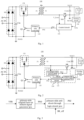
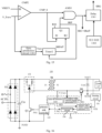
- Fig. 1 shows a structural schematic diagram of an isolated power supply system 100 according to an embodiment of the present invention.
- the isolated power supply system adopts a flyback power supply topology including a primary side and a secondary side.
- the primary side includes a rectifier bridge RB, the rectifier bridge RB has an input coupled to an external AC power source.
- the primary side further includes a primary-side winding P1 of an isolation transformer T1 and a primary-side transistor switch Q1.
- the secondary side includes a secondary-side winding S1 of the isolation transformer T1 and a synchronous rectification transistor SR.
- the isolated power supply system 100 may further include an input capacitor Cin and a snubber circuit CR both on the primary side, as well as an output filtering capacitor Cout and a load 107 both on the secondary side.
- the topological essence of such a flyback power supply is well known to those skilled in the art and therefore does not need to be described in further detail herein.
- FIG. 1 shows the use of the control circuit 101 in an isolated power supply system of a flyback topology
- the present invention is not so limited, because it may also be suitably used in any other isolated power supply topology associated with a risk of cross conduction of a primary-side transistor switch and a synchronous rectification transistor, such as for example, single-ended forward, dual-switch forward, active clamp forward, resonant half-bridge LLC, resonant full-bridge LLC, phase-shifted full-bridge, etc., as would be appreciated by those of ordinary skill in the art.
- the control circuit 101 receives a feedback signal VFB of an output voltage Vout of the isolated power supply 100 and derives therefrom a supposed turn-on instant K1 for the primary-side transistor switch Q1. It also receives a voltage signal V Forw from the secondary-side winding S1 of the isolated power supply 100 and derives a turn-off instant K2 of the secondary-side synchronous rectification transistor SR from the voltage signal V Forw from the secondary-side winding.
- the phrase "supposed turn-on instant for the primary-side transistor switch” is intended to refer to an instant of time when the primary-side transistor switch is to be turned on determined according only to the feedback control loop design principles of the isolated power supply 100 from the output voltage feedback signal VFB as well as other possible feedback parameters like an output current feedback signal, an internal clock signal and/or a feedback loop compensation.
- the supposed turn-on instant K1 for the primary-side transistor switch Q1 may be "derived" by determining it directly from information on the supposed turn-on instant K1 contained in a generated signal or by performing an operation on time instant information contained in a signal, which adds or subtracts a time bias, for example.
- the "voltage of the secondary-side winding” is a voltage at a variable potential terminal of the secondary-side winding, which is a common terminal of the synchronous rectification transistor switch SR and the secondary-side winding S1.
- the "voltage signal from the secondary-side winding” is defined as a signal that characterizes the voltage of the secondary-side winding, for example, a signal resulting from the passage of the voltage of the secondary-side winding through a voltage divider, or a signal directly sampled at the variable potential terminal of the secondary-side winding.
- the instants K1 and K2 are both mentioned as to each operational period of the respective switches. There are multiple instants K1 and K2 within multiple such operational periods. In the embodiment shown in Fig.
- the synchronous rectification transistor SR is connected between the secondary-side winding S1 and a secondary-side ground SGND so that the output voltage VOUT is directly provided at a dotted terminal of the secondary-side winding.
- the dotted terminal is a fixed potential terminal.
- a non-dotted terminal of the secondary-side winding is connected to the synchronous rectification transistor SR, and the voltage of the secondary-side winding is present at the non-dotted terminal.
- the synchronous rectification transistor SR may be alternatively connected between the secondary-side winding and an output of the isolated power supply 100, as shown in Fig. 1 . In this case, the voltage of the secondary-side winding is present at the dotted terminal.
- the control circuit 101 is further configured to derive an actual turn-on instant for the primary-side transistor switch Q1 from both the supposed turn-on instant K1 for the primary-side transistor switch Q1 and the turn-off instant K2 of the secondary-side synchronous rectification transistor and to generate a primary-side transistor switch control signal PSC.
- the actual turn-on instant for the primary-side transistor switch Q1 corresponds to the supposed turn-on instant K1.
- the actual turn-on instant for the primary-side transistor switch is delayed to be not earlier than the turn-off instant K2 of the secondary-side synchronous rectification transistor.
- the control circuit 101 independently determines the turn-off instant K2 of the secondary-side synchronous rectification transistor without detecting whether the primary-side transistor switch is ON or not, and then takes the turn-off instant K2 of the secondary-side synchronous rectification transistor as a basis for determining the actual turn-on instant for the primary-side transistor switch, achieving the purpose of avoiding shoot-through without delaying the primary-side transistor switch control signal.
- a control feedback loop in the control circuit 101 for the primary-side transistor switch Q1 may perform feedback control computation to choose to determine the actual turn-on instant for the primary-side transistor switch based on the supposed turn-on instant K1 without any additional delaying processing.
- the anti-shoot-through design does not affect feedback response or circuit performance at all.
- the primary-side transistor switch Q1 may be turned on following the turning off of the secondary-side synchronous rectification transistor only when such a risk of shoot-through has been confirmed. This eliminates the possibility of shoot-through, and since the control circuit only precisely intervenes and modifies the turn-on instant for the primary-side transistor switch rarely in some periods found to be with a high risk of shoot-through, only exerting a limited impact on the feedback response performance.
- control circuit 101 is a secondary-side controller entirely incorporated in the secondary side of the isolated power supply 100.
- the primary-side transistor switch control signal PSC may be an electrical level signal, which turns on the primary-side transistor switch, for example, by its rising edge.
- the primary-side transistor switch control signal PSC may further contain information on a turn-off instant of the primary-side transistor switch and may turn off the primary-side transistor switch, for example, by its falling edge. In this way, the primary-side transistor switch control signal PSC contains all information for turning on or off the primary-side transistor switch Q1 and is able to turn on or off the primary-side transistor switch Q1.
- control circuit 101 may further output a drive signal SRG for turning on or off the secondary-side synchronous rectification transistor SR.
- the drive signal SRG may be generated from the voltage signal V Forw from the secondary-side winding. More details in control of the secondary-side synchronous rectification transistor SR and an associated circuit arrangement will be set forth below.
- the isolated power supply 100 further includes a primary-side controller 105 and a sensing circuit 106.
- the primary-side controller 105 is arranged on the primary side and configured to receive the primary-side transistor switch control signal PSC and generate, from information contained therein on the turn-on instant for the primary-side transistor switch, a primary-side transistor switch drive signal PSG
- the primary-side controller 105 may directly generate the primary-side transistor switch drive signal PSG from the primary-side transistor switch control signal PSC.
- the primary-side controller 105 may determine the turn-off instant of the primary-side transistor switch further based on any other suitable feedback signal, such as for example, a signal indicative of a detected current through the primary-side transistor switch, or a demagnetization signal present at a drain of the primary-side transistor switch.
- any suitable feedback signal such as for example, a signal indicative of a detected current through the primary-side transistor switch, or a demagnetization signal present at a drain of the primary-side transistor switch.
- Those of ordinary skill in the art may design the circuit to determine the turn-off instant of the primary-side transistor switch using any suitable signal according to the actual requirements and feedback characteristics, and the present invention is not limited in this regard.
- the sensing circuit 106 is configured to sense the secondary-side output voltage VOUT and generate the feedback signal VFB.
- the sensing circuit 106 may be a separate component from the control circuit 101.
- the sensing circuit 106 may be alternatively integrated with the control circuit 101 in a single die or chip.
- common examples of the sensing circuit 106 may include a resistive voltage divider, and a further detailed description thereof is omitted herein.
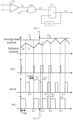
- Fig. 2 shows a detailed block diagram of the control circuit 101 according to an embodiment of the present invention.
- the control circuit 101 includes a secondary-side control signal generator 102 configured to receive the voltage signal V_Forw from the secondary-side winding in the isolated power supply and generate a secondary-side transistor switch control signal SRoff, which contains information on the turn-off instant K2 of the secondary-side synchronous rectification transistor SR for turning off the secondary-side synchronous rectification transistor SR.
- the secondary-side transistor switch control signal SRoff is not necessarily used to drive the secondary-side synchronous rectification transistor SR.
- the secondary-side transistor switch control signal SRoff may be directly used as the drive signal SRG for the secondary-side synchronous rectification transistor SR to act on a gate of the secondary-side synchronous rectification transistor SR to turn it off.
- SRoff may be an intermediate signal, and the drive signal SRG for driving the secondary-side synchronous rectification transistor may be generated from the intermediate signal.
- SRoff and the final drive signal SRG for the secondary-side synchronous rectification transistor may be derived from a common source signal containing information on the turn-off instant K2 of the secondary-side synchronous rectification transistor SR or all the parameters required to derive the turn-off instant K2 of the secondary-side synchronous rectification transistor SR.
- SRoff is generated earlier than SRG, the turn-off instant K2 of the synchronous rectification transistor indicated in SRoff is a theoretical value, which may be slightly earlier than an actual turn-off instant of the secondary-side synchronous rectification transistor.
- the purpose of the present invention can be achieved as long as SRoff contains information on the turn-off instant K2 of the secondary-side synchronous rectification transistor.
- the secondary-side control signal generator 102 may employ any common conventional independent control approach to turn off the synchronous rectification transistor SR based on the received voltage signal V Forw from the secondary-side winding in the isolated power supply without needing to detect whether the primary-side transistor switch Q1 is ON or not.
- any common conventional independent control approach to turn off the synchronous rectification transistor SR based on the received voltage signal V Forw from the secondary-side winding in the isolated power supply without needing to detect whether the primary-side transistor switch Q1 is ON or not.
- those of ordinary skill in the art may select a suitable conventional method and associated parameters to enable the secondary-side control signal generator 102 to substantially ensure the avoidance of cross conduction of the synchronous rectification transistor SR and the primary-side transistor switch Q1 when in steady-state operation even without an anti-shoot-through or anti-breakdown design.
- the secondary-side control signal generator 102 may turn off the synchronous rectification transistor SR following zeroing of the inductor current in order to avoid oscillation caused by ongoing conduction of the synchronous rectification transistor SR following zero-crossing.
- this design is still insufficient in effective avoidance of shoot-through and breakdown. More details of the secondary-side control signal generator 102 will be set forth in the following descriptions.
- the control circuit 101 further includes a primary-side control signal generator 103 configured to receive the secondary-side transistor switch control signal SRoff and the feedback signal VFB of the isolated power supply's output voltage and generate therefrom the primary-side transistor switch control signal PSC that indicates the turn-on instant for the primary-side transistor switch.
- the primary-side control signal generator 103 determines a second turn-on instant K2 (i.e., the aforementioned turn-off instant K2 of the secondary-side synchronous rectification transistor) based on the secondary-side transistor switch control signal.
- the primary-side control signal generator 103 determines a first turn-on instant K1 (i.e., the aforementioned supposed turn-on instant for the primary-side transistor switch) based on the feedback signal VFB of the isolated power supply's output voltage. The primary-side control signal generator 103 further determines the actual turn-on instant for the primary-side transistor switch based on the second turn-on instant K2 or the first turn-on instant K1, whichever is later, and thereby generates the primary-side transistor switch control signal PSC.
- K1 i.e., the aforementioned supposed turn-on instant for the primary-side transistor switch
- the second turn-on instant K2 is just the turn-off instant of the secondary-side synchronous rectification transistor indicated in the signal SRoff as it was generated.
- SRoff may be delayed by an amount depending on the actual design and wiring requirements, creating a slight difference between the second turn-on instant to be compared and the turn-off instant of the secondary-side synchronous rectification transistor indicated in the signal SRoff as it was generated. As the delay amount is very slight and can be ignored, the second turn-on instant can be stilled considered as the turn-off instant of the secondary-side synchronous rectification transistor.
- the control circuit 101 is a secondary-side controller entirely incorporated in the secondary side and further includes a primary-side control signal transmission circuit 104 for receiving the primary-side transistor switch control signal PSC, modulating the signal PSC and transmitting it from the secondary side to the primary side.
- the primary-side control signal transmission circuit 104 may employ any common technique for isolated communication between the primary and secondary sides, such as for example, optical coupling, magnetic coupling, capacitive coupling or on-off keying (OOK), and the modulated primary-side transistor switch control signal PSC may be transmitted in the form of a pulse signal.
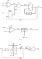
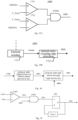
- Fig. 3 shows a structural schematic block diagram of the primary-side control signal generator 103 according to an embodiment of the present invention.
- the primary-side control signal generator 103 may include a primary-side original turn-on instant signal generator 301 and a primary-side anti-shoot-through logic circuit 302.
- the primary-side original turn-on instant signal generator 301 may receive the feedback signal VFB of the output voltage of the isolated power supply 100 and generate a primary-side original turn-on instant signal PSO indicating the supposed turn-on instant for the primary-side transistor switch (i.e., the first turn-on instant K1).
- the primary-side anti-shoot-through logic circuit 302 may receive the primary-side original turn-on instant signal PSO and the secondary-side transistor switch control signal SRoff (indicating the second turn-on instant K2), and if the first turn-on instant K1 is later than the second turn-on instant K2, generate the primary-side transistor switch control signal PSC based on the secondary-side transistor switch control signal SRoff so that the turn-on instant for the primary-side transistor switch for the current period is not earlier than the second turn-on instant.
- Fig. 4 shows a detailed structural schematic diagram of the primary-side control signal generator 103 according to an embodiment of the present invention.
- the primary-side control signal generator may control the primary-side transistor switch by an on-time (COT) feedback control design.
- the primary-side original turn-on instant signal generator 301 may include a first comparison block CMP1 configured to compare the feedback signal VFB of the isolated power supply's output voltage with a first reference Vref1, and upon the feedback signal VFB of the isolated power supply's output voltage dropping to the first reference Vref1, generate the primary-side original turn-on instant signal PSO indicating the supposed turn-on instant for the primary-side transistor switch.
- the secondary-side transistor switch control signal may be an electrical level signal
- the primary-side anti-shoot-through logic circuit 302 may include a first logic gate receiving PSO and SRoff.
- the primary-side original turn-on instant signal PSO indicates that it is suitable to turn on the primary-side transistor switch Q1 and if the secondary-side transistor switch control signal SRoff indicates that the turn-off instant K2 of the secondary-side synchronous rectification transistor SR has arrived
- the first logic gate may output a primary-side transistor switch turn-on instant signal PON indicative of the arrival of the turn-on instant for the primary-side transistor switch.
- the first logic gate may be a first AND gate AND1 having two inputs and one output.
- the primary-side original turn-on instant signal PSO may be received at the first input, and an inverted version of the secondary-side transistor switch control signal SRoff may be received at the second input.
- the primary-side transistor switch turn-on instant signal PON may be output from the output of the first AND gate AND1.
- the primary-side transistor switch turn-on instant signal PON may also contain information on the turn-on instant for the primary-side transistor switch Q1.
- the primary-side transistor switch turn-on instant signal PON may be directly taken as the primary-side transistor switch control signal PSC.
- the primary-side transistor switch turn-on instant signal PON may be taken as a basis for generating the primary-side transistor switch control signal PSC.
- the primary-side control signal generator may further include a first flip-flop RS 1 having a set terminal S, a reset terminal R and an output terminal Q.
- the primary-side transistor switch turn-on instant signal PON may be received at the set terminal S, and the primary-side transistor switch control signal PSC may be responsively output from the output terminal.
- the embodiment shown in Fig. 4 may further include a primary-side on-time timer Timer 1 with an output connected to the reset terminal R of the first flip-flop RS 1.
- the timer may start to count down a predetermined period of time Tonp based on the information on the turn-on instant for the primary-side transistor switch and output a reset signal to the reset terminal R of the first flip-flop RS 1 upon the expiry of the period.
- Tonp may be an on-time length of the primary-side transistor switch.
- the primary-side on-time timer Timer 1 may be triggered by any signal containing information on the turn-on instant for the primary-side transistor switch. For example, in the embodiment shown in Fig.
- the primary-side on-time timer Timer1 may obtain information on the turn-on instant for the primary-side transistor switch from the primary-side transistor switch control signal PSC received at its input.
- the primary-side on-time timer Timer1 may directly receive the primary-side transistor switch turn-on instant signal PON and obtain information on the turn-on instant for the primary-side transistor switch therefrom.
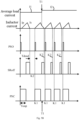
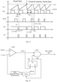
- Figs. 5A and 5B show operating waveforms of the primary-side control signal generator 103 according to the embodiment shown in Fig. 4 .
- the working principles of the primary-side control signal generator 103 will be described below with reference to Figs. 4, 5A and 5B as an example.
- Fig. 5A shows operating waveforms in CCM operation of the isolated power supply 100.
- a primary-side current Ip and a secondary-side current Is are shown as a single waveform collectively labeled and referred to hereafter as "inductor current".
- the term "inductor current” does not refer to a real-world current but the combined waveform of the primary-side current Ip and the secondary-side current Is. Moreover, for ease of explanation of the waveforms here and hereafter, it is presumed that an on-time length of the secondary-side synchronous rectification transistor can vary in response to loading changes. Prior to the time instant T1, the isolated power supply 100 operates in an ideal steady state at an average load current of I1, where an appropriate dead time Tdead for avoiding cross conduction of the primary-side transistor switch Q1 and the synchronous rectification transistor SR can be established simply by the COT feedback loop design of the primary-side transistor switch.
- the first AND gate AND1 receiving its inverted version outputs a high level, setting the first flip-flop RS 1.
- PSC output from the first flip-flop RS 1 is high and turns on the primary-side transistor switch.
- the primary-side on-time timer Timer 1 start to count down, and VFB rises with the inductor current. After Timer1 completes the countdown of Tonp, the first flip-flop RS 1 is reset, and PSC is low and turns off the switch.
- the synchronous rectification transistor SR is then turned on to start freewheeling, and VFB decreases with inductor current. Throughout this period, SRoff does not affect the turn-on instant for the primary-side transistor switch at all, and K1 is just the theoretical turn-on instant for the primary-side transistor switch. The final actual turn-on instant for the primary-side transistor switch depends only on an inherent delay caused by the transmission of PSC for forming PSG that turns on the primary-side transistor switch without introducing any additional delay, and excellent feedback performance is obtained.
- the average load current jumps from I1 to 12 that is higher, and the isolated power supply 100 starts to operate in a transient response state. Due to the rise in load current, VFB sharply drops to VREF1, causing PSO to transition high.
- Fig. 5B shows operating waveforms in DCM operation of the isolated power supply 100.
- the synchronous rectification transistor SR is turned off following zeroing of the inductor current in order to avoid the occurrence of oscillation.
- SRoff will become low at the same time. Therefore, whether the isolated power supply 100 is in a steady state or has entered a transient response state following an abrupt change in the load current, the presence of a zero-current interval makes it sure that SRoff drop low earlier than a drop of VFB to VREF1.
- K1 is also simply the theoretical turn-on instant for the primary-side transistor switch.
- the final actual turn-on instant for the primary-side transistor switch also depends only on an inherent delay caused by the transmission of PSC for forming PSG that turns on the primary-side transistor switch without introducing any additional delay, and excellent feedback performance is also obtained.
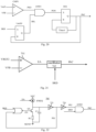
- Fig. 6 shows a detailed structural schematic diagram of the primary-side control signal generator 103 according to another embodiment of the present invention.
- the embodiment shown in Fig. 6 differs from that of Fig. 4 in that the secondary-side transistor switch control signal SRoff is a pulse signal.
- the primary-side anti-shoot-through logic circuit 402 further includes a first latch Latch 1 for latching the received secondary-side transistor switch control signal SRoff and outputting the latched signal SRL.
- the latch Latch1 is implemented as an RS flip-flop.
- the primary-side original turn-on instant signal PSO and the latched signal SRL are respectively received at the two inputs of the first AND gate AND1 that serves as the first logic gate, and the primary-side transistor switch turn-on instant signal PON is output from the first AND gate AND1.
- the primary-side transistor switch control signal PSC output from the first flip-flop RS1 is also provided to the first latch Latch1 in order to reset the first latch Latch1 based on information on the turn-on instant for the primary-side transistor switch.
- the first latch Latch1 is not limited to being resettable only by the primary-side transistor switch control signal PSC. Instead, it can be reset by any signal containing information on the turn-on instant for the primary-side transistor switch.
- Fig. 7 shows a structural schematic diagram of the primary-side control signal generator 103 according to yet another embodiment of the present invention. As shown in Fig.
- the secondary-side transistor switch control signal SRoff may be asserted to enable the primary-side control signal generator 103 or not, and the second turn-on instant K2 may be a time instant when the secondary-side transistor switch control signal SRoff is asserted to enable the primary-side control signal generator 103.
- the primary-side control signal generator 103 shown in Fig. 7 may include a first error amplifier 701 and an oscillator 702.
- the first error amplifier 701 may be configured to amplify a difference between the feedback signal VFB of the isolated power supply's output voltage and a second reference VREF2 and output an amplified error signal EA.
- the oscillator 702 may receive the amplified error signal EA and the secondary-side transistor switch control signal SRoff and generate a square wave signal as the primary-side transistor switch control signal PSC.
- a frequency of the square wave signal may be determined by the amplified error signal EA, and a rising or falling edge thereof may indicate the turn-on instant for the primary-side transistor switch.
- the oscillator 702 may delay the rising or falling edge of the square wave signal to a time instant not earlier than the instant K2 when the secondary-side transistor switch control signal SRoff is asserted.
- the time instant determined as the instant of supposed arrival of the edge of the square wave signal by the oscillator 702 based on the current frequency may be the first turn-on instant K1, and the oscillator 702 may check whether the enable signal EN (i.e., SRoff) is asserted at the first turn-on instant K1.
- Fig. 8 shows a structural schematic diagram of the oscillator 702 according to one of such embodiments.
- the oscillator 702 may include: a frequency setting current source 721 for generating a frequency setting current IFREQ based on the amplified error signal EA; a frequency setting capacitor C1 having a first terminal for receiving the frequency setting current IFREQ and a second terminal for receiving the reference ground SGND; a discharge branch 722 including, in the illustrated embodiment, a discharge control switch Q3 and a discharge resistor R1, which are connected in series to both terminal of the frequency setting capacitor C1, the discharge control switch Q3 being controlled by an enable signal EN; a first hysteresis inverter 723 with an input connected to the first terminal of the frequency setting capacitor C1; a second hysteresis inverter 724 with an input connected to an output of the first hysteresis inverter 723; an enable NOR gate 725 having a first input receiving the secondary-side transistor switch control signal SRoff, a second input connected to an output of the first hysteresis inverter and an output for outputting the
- the discharge branch 722 is not limited to being implemented as the series discharge control switch Q3 and discharge resistor R1 as in the illustrated embodiment.
- the discharge resistor R1 may be replaced with a discharge current source.
- the discharge branch 722 may start or stop discharging under the control of the enable signal EN and may form, together with the frequency setting capacitor C1, a discharge loop with a capacitive time constant.
- the capacitive time constant may be adjusted as needed by changing the resistance of R1 or a current from the discharge current source to allow the discharge branch 722 to achieve a desired discharge time, thereby resulting in a change in the on-time duration of the primary-side transistor switch to which the primary-side transistor switch control signal PSC corresponds.
- Fig. 9 shows operating waveforms of the oscillator according to the embodiment shown in Fig. 8 .
- upper and lower thresholds for the first hysteresis inverter are VCC and SGND potentials, respectively.
- the secondary-side transistor switch control signal SRoff contains information on both the turn-on and turn-off time instants for the secondary-side synchronous rectification transistor and the on-time length of the secondary-side synchronous rectification transistor is variable.
- the frequency setting current source changes C1 at IFREQ set based on the output signal EA.
- a voltage VC1 across both ends of C1 gradually increases and when it reaches the upper threshold VCC for the first hysteresis inverter 723, the first hysteresis inverter outputs a low level electrical signal PS 1 and the second hysteresis inverter 724 outputs a high level electrical signal PS2.
- PS 1 and PS2 indicate the supposed turn-on instant K1 for the primary-side transistor switch (i.e., the first turn-on instant).
- the discharge period of time Tdis is the on-time length Tonp of the primary-side transistor switch.
- EA causes an increase in IFREQ, allowing the voltage across both ends of C1 to reach the upper threshold VCC of the first hysteresis inverter 723 in a shorter time when compared to the case of steady-state operation.
- the first hysteresis inverter 723 then transitions to a low level, indicating the arrival of the supposed turn-on instant K1 for the primary-side transistor switch.
- the oscillator 702 may determine a supposed time instant of arrival of the edge of the square wave signal based on the current frequency as the first turn-on instant K1, and check prior to the first turn-on instant K1 whether the enable signal EN (i.e., SRoff) is asserted. This can additionally avoid cross conduction of the primary-side transistor switch and the secondary-side synchronous rectification transistor under extreme conditions.
- Fig. 10 shows a schematic circuit diagram of the oscillator 702 according to one of such embodiments.
- an edge detection circuit 824 is included in place of the second hysteresis inverter 724 and the second AND gate AND2 in the embodiment of Fig. 8 .
- an input of the edge detection circuit 824 is connected to the output of the first hysteresis inverter 723 and configured to detect a rising edge, and an output of the edge detector 824 provides the primary-side transistor switch control signal PSC.
- edge detection circuit 824 has been described and illustrated in Fig. 10 as being configured to detect a rising edge of the output signal PS 1 of the first hysteresis inverter 723, in other embodiments, the edge detection circuit 824 may be alternatively configured to determine the primary-side transistor switch control signal PSC based on a detection of a falling edge of PS1. The latter case actually checks whether the enable signal EN is asserted at the same time as the arrival of the first turn-on instant K1. Further, in order to address various actual applications with different reliability requirements, appropriate selections may be made from the signal detection modes and the rising and falling edges.
- Fig. 11 shows operating waveforms according to the embodiment of Fig. 10 .
- the first hysteresis inverter 723 transitions from low to high, creating a rising edge on PS1
- the edge detector 824 responsively outputs a single trigger pulse as the primary-side transistor switch control signal PSC, indicating the arrival of the turn-on instant for the primary-side transistor switch.
- the voltage across both ends of C1 reaches the lower threshold SGND, and a rising edge accordingly appears on PS1 from the first hysteresis inverter 723, indicating the arrival of the instant K1.
- the edge detector 824 the signal PSC indicates the arrival of the turn-on instant for the primary-side transistor switch.
- the falling edge of the output signal of the first hysteresis inverter 723 will arrive at an earlier time. In this case, the falling edge K1-Tdis is earlier than the turn-off instant of the secondary-side synchronous rectification transistor indicated in SRoff.
- edge detector 824 does not output a pulse to turn on the primary-side transistor switch.
- the enable signal EN enables the discharge branch 722 until SRoff indicates the arrival of the turn-off instant of the secondary-side synchronous rectification transistor, and the rising edge of the output signal of the first hysteresis inverter 723 arrives after the discharge period of time Tdis (i.e., K2+Tdis).
- the edge detector 824 outputs a pulse signal as PSC, indicating the turn-on instant for the primary-side transistor switch, i.e., K2+Tdis.
- the supposed turn-on instant K1 for the primary-side transistor switch (i.e., first turn-on instant) is the instant of arrival of the falling edge of the output signal PS 1 of the first hysteresis inverter 723 plus the discharge period of time Tdis.
- Tdis provides a buffer for decision-making.
- the on-time length Tonp of the primary-side transistor switch is in no relation to Tdis, but may be instead determined by a width of the output pulse of the edge detector 824, as shown in the figure.
- the output pulse of the edge detector 824 may only determine the turn-on instant for Q1, and Tonp may be generated by another suitable mechanism such as, for example, timing or Q1 current peak detection.
- the secondary-side control signal generator 102 may also employ COT control.
- the secondary-side control signal generator 102 receives the voltage signal V Forw from the secondary-side winding. If the voltage signal V_Forw from the secondary-side winding is equal to a third reference VREF3, the secondary-side control signal generator 102 turns on the secondary-side synchronous rectification transistor and starts counting down a first predetermined period of time Tson. After the elapse of the period, the secondary-side control signal generator 102 generates the secondary-side transistor switch control signal SRoff indicating the turn-off instant K2 of the secondary-side synchronous rectification transistor.
- the first predetermined period of time Tson may be either fixed or variable.
- the secondary-side control signal generator 102 may further determine, from the voltage signal V Forw from the secondary-side winding, whether the secondary-side inductor current is in a zero-current interval following a zero-crossing. If it is in a zero-current interval, no matter the countdown of the first predetermined period of time Tson is complete or not, the secondary-side transistor switch control signal SRoff indicating the turn-off instant K2 of the secondary-side synchronous rectification transistor will be generated. In this way, SRoff can take account into both CCM operation and DCM operation through using a COT turn-off mode in CCM operation and using a timely turn-off mode following a zero-crossing of the inductor current in DCM operation.
- the secondary-side transistor switch control signal SRoff can further contain turn-on information of the secondary-side synchronous rectification transistor, the signal SRoff thus serves as a secondary-side transistor switch drive signal for directly driving the secondary-side synchronous rectification transistor, or the signal SRoff is used as a basis for generating such a secondary-side synchronous rectification transistor drive signal.
- the turn-on information of the secondary-side synchronous rectification transistor contained in the secondary-side transistor switch control signal SRoff may be further used to indicate the turn-on of the secondary-side synchronous rectification transistor and thus start a timer.
- Fig. 12 shows a structural schematic diagram of the secondary-side control signal generator 102 according to an embodiment of the present invention.
- the secondary-side control signal generator may include a second comparator CMP2, a second flip-flop RS2 and a secondary-side control timer Timer2.
- the second comparator CMP2 may have a first input, a second input and an output.
- the first input receives the voltage signal V Forw from the secondary-side winding
- the second input receives the third reference VREF3, and the output provides a signal CMP_S.
- the second flip-flop RS2 may have a set terminal S2, a reset terminal R2 and an output terminal Q2.
- the set terminal S2 of the second flip-flop may be connected to the output of the second comparator CMP2.
- the secondary-side control timer Timer2 may have a timer starter terminal and a timing result output terminal.
- the timer starter terminal may start a timer upon the secondary-side synchronous rectification transistor being turned on, and a timing result may be output to the reset terminal R2 of the second flip-flop upon the elapse of the first predetermined period of time Tson.
- a signal SRP output from the output terminal Q2 of the second flip-flop RS2 may be received at the timer starter terminal of the secondary-side control timer Timer2 as an indication that the secondary-side synchronous rectification transistor has been turned on and it is suitable to start a timer.
- the output signal CMP_S of the second comparator CMP2 may be used to indicate the turning on of the secondary-side synchronous rectification transistor and to initiate a timer.
- the output signal CMP_S of the second comparator CMP2 may be directly coupled to the timer starter terminal of the secondary-side control timer Timer2.
- any signal containing turn-off information of the secondary-side synchronous rectification transistor may be used as the secondary-side transistor switch control signal SRoff.
- the output signal SRP of the second flip-flop RS2 may serve as the secondary-side transistor switch control signal SRoff.
- a signal SRPoff output from the timing result output terminal of the secondary-side control timer Timer2 may be used as the secondary-side transistor switch control signal SRoff.
- the signal output from the timing result output terminal may be a single pulse signal.
- the secondary-side control signal generator 102 may further include a third AND gate AND3 with two inputs and one output. The two inputs may be connected respectively to the output of the second comparator CMP2 and the output terminal Q2 of the second flip-flop.
- an output signal SRC of the third AND gate AND3 may be taken as the secondary-side transistor switch control signal SRoff.
- V Forw is approximately equal to the secondary-side ground potential and is always lower than VREF3.
- the second comparator CMP3 may output a high level to the third AND gate AND3 so that the output of the third AND gate AND3 depends solely on the output terminal Q2 of the second flip-flop RS2.
- the timing result determines the output of the third AND gate AND3.
- the timing result determines the output of the third AND gate AND3.
- the secondary-side control signal generator 102 may generate the aforementioned secondary-side synchronous rectification transistor drive signal SRG
- SRC SRG
- SRG may also be generated indirectly from SRC.
- the secondary-side control signal generator 102 may further include a synchronous rectification time prediction circuit 1201, which allows a more accurate turn-off instant of the secondary-side synchronous rectification transistor in steady-state operation, an optimized dead time and improved efficiency, as well as enhanced transient response performance achieved through enabling the primary-side transistor switch to be turned on at a supposed turn-on instant under most loading conditions.
- the synchronous rectification time prediction circuit 1201 may be configured to predict a turn-off instant of the synchronous rectification transistor and generate the first predetermined period of time Tson in a flexible way.
- the synchronous rectification time prediction circuit 1201 may output information on the first predetermined period of time Tson that represents an on-time length of the secondary-side synchronous rectification transistor to the secondary-side control timer Timer2.
- the synchronous rectification time prediction circuit 1201 may generate, from the voltage signal V Forw from the secondary-side winding received at an input thereof, the first predetermined period of time Tson, and determine a turn-off instant of the synchronous rectification transistor SR as the time after the elapse of Tson following the turn-on of the synchronous rectification transistor SR.
- Tson may be generated based on the current switching frequency derived from the signal CMP_S received by the time prediction circuit. A description of particular algorithms used is omitted here for the sake of brevity.
- Fig. 13 shows a detailed structural schematic diagram of the isolated power supply control circuit 101 according to another embodiment of the present invention.
- the isolated power supply control circuit 101 further includes a first delay circuit 1301, the first delay circuit 1301 is configured to delay the turn-off instant of the secondary-side synchronous rectification transistor in order to reduce a gap between the turn-off instant of the secondary-side transistor switch and the turn-on instant for the primary-side transistor switch, but the first delay circuit 1301 does not delay the turn-off instant of the secondary-side transistor switch indicated in the secondary-side transistor switch control signal SRoff.
- the first delay circuit 1301 may receive the output signal SRC of the third AND gate AND3, delay it and provides the delayed signal as the secondary-side synchronous rectification transistor drive signal SRG
- SRC secondary-side transistor switch control signal SRoff
- the turn-off instant of the secondary-side transistor switch indicated in SRoff may be earlier than the actual turn-off instant of the secondary-side transistor switch.
- This delay design can partially offset the delay incurred during the transmission of the generated primary-side transistor switch control signal PSC to the primary side before it actually turns on the primary-side transistor switch, thus additionally optimizing the dead time and resulting in further improved efficiency.
- the first delay circuit 1301 may be arranged at a different location than as shown in Fig. 13 , as long as it is allowed to only delay the actual turn-off instant of the secondary-side synchronous rectification transistor but not the turn-off instant of the secondary-side transistor switch indicated in the secondary-side transistor switch control signal SRoff.
- the delay created by the first delay circuit 1301 may be adjustable, and the control circuit 101 may further include a transient detection circuit 1302.
- the transient detection circuit 1302 is configured to determine whether a load jump has occurred in the isolated power supply and, if so, output to the first delay circuit a transient response signal for shortening the delay of the first delay circuit 1301.
- the actual turn-on instant for the primary-side transistor switch is principally determined by the supposed turn-on instant for the primary-side transistor switch.
- the dead time is equal to a difference between the instants indicated respectively in PSC and SRoff plus the delay incurred during the transmission of PSC to the primary side before it finally turns on the primary-side transistor switch minus the delay created by the first delay circuit 1301 and thus has a large safety margin that can be properly modulated for improved efficiency.
- the primary-side transistor switch may be turned on at an earlier time when compared with the case of steady-state operation. Consequently, the instant indicated in PSC may be substantially equal to that indicated in SRoff.
- Detection algorithms that can be used in the transient detection circuit 1302 have been described in literature, and a description thereof is omitted herein for the sake of brevity.
- Fig. 15 shows a detailed structural schematic diagram of the control circuit 101 according to a further embodiment of the present invention.
- the control circuit further includes a dead time interrogation circuit 1303.
- the dead time interrogation circuit 1303 is configured to calculate a dead time of the previous operational period and compare the calculated value with a dead time reference Tref_D. If the calculated value is less than the dead time reference Tref_D, the dead time interrogation circuit 1303 may reduce the delay provided by the first delay circuit 1301. Otherwise, if the calculated value is greater than the dead time reference Tref_D, the dead time interrogation circuit 1303 may increase the delay provided by the first delay circuit 1301.
- Such timely response of the dead time interrogation circuit 1303 can ensure that the dead time always lies in a target range, thus achieving maximized efficiency.
- Fig. 16 is a schematic diagram illustrating the architecture of the control circuit 101 according to a further embodiment of the present invention.
- the control circuit 101 shown in Fig. 16 is also applicable to the embodiment shown in Fig. 1 .
- the technical features that have been described above in conjunction with the embodiments shown in Figs. 2 to 15 and can be readily applied by those of ordinary skill in the art to the embodiment of Fig. 16 will not be described again, but they are still considered as part of the disclosure of the present invention.
- the control circuit 101 further includes a turn-off detector 1604 for the secondary-side transistor switch, which is connected in the secondary side of the isolated power supply and configured to produce a turn-off acknowledgement signal SRD when the secondary-side synchronous rectification transistor has been turned off.
- the primary-side control signal generator 103 is configured to receive the turn-off acknowledgement signal SRD and the feedback signal VFB of the isolated power supply's output voltage and responsively generate the primary-side transistor switch control signal PSC indicating the turn-on instant for the primary-side transistor switch.
- the primary-side control signal generator determines the first turn-on instant K1 based on the turn-off acknowledgement signal SRD and determines the second turn-on instant K2 based on the feedback signal VFB of the isolated power supply's output voltage.
- the primary-side control signal generator 103 further determines the turn-on instant for the primary-side transistor switch based on the second turn-on instant K2 or the first turn-on instant K1, whichever is later, and responsively generates the primary-side transistor switch control signal PSC.
- generating the signal SRD indicative of the second turn-on instant K2 based on the confirmed turn-off of the secondary-side synchronous rectification transistor is more reliable and suited to applications requiring extremely high reliability than generating it based on the signal SRoff.
- the turn-off detector 1604 for the secondary-side transistor switch may receive the voltage signal V Forw from the secondary-side winding in the isolated power supply, compare it separately with a first turn-off reference VREFD1 (corresponding to a voltage of the secondary-side winding when the synchronous rectification transistor is turned on during freewheeling) and a second turn-off reference VREFD2 (corresponding to a voltage of the secondary-side winding when a parasitic body diode is turned on after the synchronous rectification transistor is turned off), and provide the comparison results to a logic gate (e.g., an AND gate AND4).
- the logic gate may perform a logical determination and responsively output the turn-off acknowledgement signal SRD.
- the turn-off detector 1604 for the secondary-side transistor switch may further include: a current sensing circuit 1721 configured to sense a current flowing through the secondary-side synchronous rectification transistor SR and output a sensed current signal Isen characterizing the current; and a current zero-crossing edge detection circuit 1722 configured to receive the sensed current signal Isen. If the sensed current signal Isen indicates the arrival of a zero-crossing falling edge of the current through the secondary-side synchronous rectification transistor SR, it is determined that the secondary-side synchronous rectification transistor SR has been turned off, and the turn-off acknowledgement signal SRD is responsively generated.
- the turn-off detection of the secondary-side synchronous rectification transistor and the structure of the turn-off detector 1604 for the secondary-side transistor switch are not limited to those described in the two embodiments of Figs. 17A and 17B , and these embodiments are exemplary rather than limiting in nature.
- any other circuit suited to turn-off detection of the secondary-side synchronous rectification transistor SR may be used as the turn-off detector 1604 for the secondary-side transistor switch, without departing from the scope of the present invention as defined by the appended claims.
- Fig. 18 shows a structural schematic diagram of the primary-side control signal generator 103 for use in the control circuit 101 of Fig. 16 according to an embodiment of the present invention.
- the primary-side anti-shoot-through logic circuit receives the primary-side original turn-on instant signal PRO and the turn-off acknowledgement signal SRD, and the turn-off instant of the secondary-side synchronous rectification transistor indicated in the turn-off acknowledgement signal is taken as the second turn-on instant K2.
- the primary-side transistor switch control signal PSC is generated based on the turn-off acknowledgement signal SRD so that the turn-on instant for the primary-side transistor switch is not earlier than the second turn-on instant K2.
- Fig. 19 shows a detailed view of the structure of the primary-side control signal generator 103 according to a corresponding embodiment, in which the turn-off acknowledgement signal SRD is an electrical level signal.
- This embodiment differs from the embodiment shown in Fig. 4 in that the first AND gate AND1 serving as the first logic gate receive, respectively at this inputs, the primary-side original turn-on instant signal PSO and the turn-off acknowledgement signal SRD and outputs the primary-side transistor switch turn-on instant signal PON containing information on the turn-on instant for the primary-side transistor switch.
- Fig. 20 shows a detailed view of the structure of the primary-side control signal generator 103 according to another corresponding embodiment, in which the turn-off acknowledgement signal SRD is a pulse signal.
- This embodiment differs from the embodiment shown in Fig. 6 in that the latch in the primary-side anti-shoot-through logic circuit 402 receives and latches the turn-off acknowledgement signal SRD and outputs the latched signal Latch.
- Fig. 21 shows a structural schematic diagram of the primary-side control signal generator 103 according to a further embodiment of the present invention. This embodiment differs from the embodiment shown in Fig. 7 in that in the primary-side control signal generator 103, the turn-off acknowledgement signal SRD may be asserted to enable the primary-side control signal generator 103 or not, and first turn-on instant K1 may be a time instant when the turn-off acknowledgement signal SRD is asserted to enable the primary-side control signal generator 103.
- the primary-side control signal generator 103 shown in Fig. 21 differs from the embodiment shown in Fig. 7 mainly in that the turn-off acknowledgement signal SRD is asserted to enable the oscillator.
- the oscillator 702 may delay the rising or falling edge of the square wave signal to a time instant not earlier than the instant when the turn-off acknowledgement signal SRD is asserted.
- the oscillator 702 may determine a supposed time instant of arrival of the edge of the square wave signal based on the current frequency as the first turn-on instant K1, and check whether the enable signal EN is asserted upon the arrival of the first turn-on instant K1.
- Fig. 22 shows a structural schematic diagram of the oscillator 702 suitable for use in the primary-side control signal generator 103 of Fig. 21 . This differs from the embodiment shown in Fig. 8 mainly in that the enable NOR gate receives the turn-off acknowledgement signal SRD at its first input, is connected to the output of the first hysteresis inverter at the second input, and provides the enable signal EN at the output.
- the second AND gate AND2 is connected to the output of the second hysteresis inverter at its first input, receives an inverted version of the turn-off acknowledgement signal SRD at the second input, and provides the primary-side transistor switch control signal PSC at the output.
- the oscillator 702 may determine a supposed time instant of arrival of the edge of the square wave signal based on the current frequency as the first turn-on instant K1, and check whether the enable signal EN is asserted prior to the arrival of the first turn-on instant K1.
- Fig. 23 shows another structural schematic diagram of the oscillator 702 suitable for use in the primary-side control signal generator 103 of Fig. 21 . This differs from the embodiment shown in Fig. 10 mainly in that the enable NOR gate receives the turn-off acknowledgement signal SRD at its first input, is connected to the output of the first hysteresis inverter at the second input, and provides the enable signal EN at the output.
- the secondary-side control signal generator 102 may similarly receive the voltage signal V_Forw from the secondary-side winding, and if the voltage signal V Forw from the secondary-side winding is equal to the third reference REF3, indicate the arrival of the turn-on instant for the secondary-side synchronous rectification transistor SR and start counting down the first predetermined period of time Tson.
- the secondary-side synchronous rectification transistor After the elapse of the first predetermined period of time Tson, it may indicate the turn-off instant of the secondary-side synchronous rectification transistor, and generate the secondary-side synchronous rectification transistor drive signal SRG based on the turn-on and turn-off instants of the secondary-side synchronous rectification transistor.
- the secondary-side control signal generator may directly employ the structure according to the embodiment shown in Fig. 12 and, in this case, is suitable for use in the control circuit 101 shown in Fig. 16 .
- the output signal of the second comparator CMP2 or the second flip-flop RS2 may contain information on the turn-on instant for the secondary-side synchronous rectification transistor and used to start a timer.
- the final secondary-side synchronous rectification transistor drive signal may be output from the third AND gate AND3, or from the second flip-flop RS2 in absence of the third AND gate AND3.
- the secondary-side control signal generator may directly employ the structure according to the embodiment shown in Fig. 15 and, in this case, is suitable for use in the control circuit 101 shown in Fig. 16 .
- the synchronous rectification time prediction circuit additionally included in the embodiment of Fig. 15 has been described above, and a repeated description thereof is omitted here.
- Fig. 24 shows a flowchart of a method 2400 for control of the isolated power supply according to embodiments of the present invention, including the steps of:
- the actual turn-on instant for the primary-side transistor switch corresponds to the supposed turn-on instant K1.
- the actual turn-on instant for the primary-side transistor switch is delayed to an instant not earlier than the turn-off instant K2 of the secondary-side synchronous rectification transistor.
Landscapes
- Engineering & Computer Science (AREA)
- Power Engineering (AREA)
- Dc-Dc Converters (AREA)
- Rectifiers (AREA)
- Apparatus For Radiation Diagnosis (AREA)
- Emergency Protection Circuit Devices (AREA)
Applications Claiming Priority (2)
| Application Number | Priority Date | Filing Date | Title |
|---|---|---|---|
| CN202011496777.3A CN113162390B (zh) | 2020-12-17 | 2020-12-17 | 隔离型电源的控制电路、隔离型电源及其控制方法 |
| PCT/CN2021/134583 WO2022127589A1 (zh) | 2020-12-17 | 2021-11-30 | 隔离型电源的控制电路、隔离型电源及其控制方法 |
Publications (2)
| Publication Number | Publication Date |
|---|---|
| EP4266564A1 true EP4266564A1 (de) | 2023-10-25 |
| EP4266564A4 EP4266564A4 (de) | 2024-06-12 |
Family
ID=76882590
Family Applications (1)
| Application Number | Title | Priority Date | Filing Date |
|---|---|---|---|
| EP21905518.3A Pending EP4266564A4 (de) | 2020-12-17 | 2021-11-30 | Steuerschaltung für isolierte stromversorgung sowie isolierte stromversorgung und steuerverfahren dafür |
Country Status (5)
| Country | Link |
|---|---|
| US (2) | US11929684B2 (de) |
| EP (1) | EP4266564A4 (de) |
| CN (1) | CN113162390B (de) |
| TW (1) | TWI796054B (de) |
| WO (1) | WO2022127589A1 (de) |
Families Citing this family (15)
| Publication number | Priority date | Publication date | Assignee | Title |
|---|---|---|---|---|
| CN113162390B (zh) * | 2020-12-17 | 2022-05-10 | 上海晶丰明源半导体股份有限公司 | 隔离型电源的控制电路、隔离型电源及其控制方法 |
| CN112532047B (zh) * | 2021-02-18 | 2021-04-16 | 上海芯龙半导体技术股份有限公司 | 开关电源芯片及系统 |
| US12431816B1 (en) * | 2021-11-18 | 2025-09-30 | Microchip Technology Incorporated | Secondary-side flyback converter controller |
| CN115149811B (zh) * | 2022-03-09 | 2026-03-03 | 杰华特微电子股份有限公司 | 反激变换器及其启动控制方法 |
| CN114785167B (zh) * | 2022-03-23 | 2023-04-07 | 电子科技大学 | 一种可控整流电路及其稳压控制方法 |
| CN115360923A (zh) * | 2022-09-19 | 2022-11-18 | 昂宝电子(上海)有限公司 | 离线式反激变换器系统及其同步整流控制器 |
| CN115694197A (zh) * | 2022-10-09 | 2023-02-03 | 中关村芯海择优科技有限公司 | 隔离式电源控制芯片及其控制方法和计算机可读存储介质 |
| CN115566898B (zh) * | 2022-11-03 | 2026-03-24 | 东南大学 | 一种应用于恒定导通时间控制的多相高精度均流控制方法 |
| US12231052B2 (en) * | 2022-12-20 | 2025-02-18 | Power Integrations, Inc. | Enable circuit with winding signal detection |
| CN116094331B (zh) * | 2022-12-28 | 2026-03-24 | 深圳市创芯微微电子有限公司 | 控制电路、控制芯片和电源适配设备 |
| CN116865525A (zh) * | 2023-05-26 | 2023-10-10 | 上海新进芯微电子有限公司 | 开关电源的待机方法、开关电源、原边和副边控制电路 |
| CN119231941A (zh) * | 2023-06-29 | 2024-12-31 | 上海晶丰明源半导体股份有限公司 | 隔离型电源及其控制电路和控制方法 |
| CN116683775B (zh) * | 2023-07-14 | 2025-07-18 | 德氪微电子(深圳)有限公司 | 一种开关电源 |
| CN117713782B (zh) * | 2024-02-04 | 2024-04-26 | 成都电科星拓科技有限公司 | 上电复位电路 |
| CN119326982B (zh) * | 2024-08-21 | 2025-11-07 | 深圳市安保医疗科技股份有限公司 | 一种输注泵抗干扰控制系统及控制方法 |
Family Cites Families (27)
| Publication number | Priority date | Publication date | Assignee | Title |
|---|---|---|---|---|
| US7321498B2 (en) * | 2005-10-31 | 2008-01-22 | Honeywell International, Inc. | DC-DC converter having synchronous rectification without cross conduction |
| US7385832B2 (en) | 2006-07-03 | 2008-06-10 | Semiconductor Components Industries, L.L.C. | Method of forming a secondary-side controller and structure therefor |
| CN101517878B (zh) * | 2006-10-02 | 2012-02-08 | 株式会社村田制作所 | 双端绝缘型dc-dc转换器 |
| CN102342007B (zh) | 2009-01-19 | 2015-01-07 | 伟创力国际美国公司 | 用于功率转换器的控制器 |
| CN103887980B (zh) * | 2014-03-13 | 2016-10-05 | 昂宝电子(上海)有限公司 | 用于调节电源变换系统的系统和方法 |
| US9374011B2 (en) | 2013-01-22 | 2016-06-21 | Power Integrations, Inc. | Secondary controller for use in synchronous flyback converter |
| KR20150095181A (ko) * | 2014-02-11 | 2015-08-20 | 페어차일드코리아반도체 주식회사 | 공진형 컨버터 및 그 구동 방법 |
| US20150326103A1 (en) * | 2014-05-08 | 2015-11-12 | Fairchild Korea Semiconductor Ltd. | Switch control circuit and power supply device including the same |
| TWI543518B (zh) * | 2014-12-31 | 2016-07-21 | 力林科技股份有限公司 | 具省電與高轉換效率機制的電源轉換裝置 |
| JP6633863B2 (ja) * | 2015-08-07 | 2020-01-22 | ローム株式会社 | 絶縁同期整流型dc/dcコンバータ、同期整流コントローラ、それを用いた電源装置、電源アダプタおよび電子機器、同期整流コントローラの制御方法 |
| TWI558077B (zh) * | 2015-08-10 | 2016-11-11 | 杰力科技股份有限公司 | 電源轉換裝置 |
| US10868473B2 (en) * | 2015-11-30 | 2020-12-15 | Semiconductor Components Industries, Llc | Secondary side controlled control circuit for power converter with synchronous rectifier |
| US10027235B2 (en) * | 2016-02-02 | 2018-07-17 | Fairchild Semiconductor Corporation | Self-tuning adaptive dead time control for continuous conduction mode and discontinuous conduction mode operation of a flyback converter |
| CN106026712B (zh) * | 2016-07-15 | 2018-05-29 | 深圳南云微电子有限公司 | 开关电源的副边控制方法及电路 |
| US10333417B2 (en) * | 2017-04-10 | 2019-06-25 | Delta Electronics (Shanghai) Co., Ltd | Device and method for controlling flyback converter |
| US10186976B2 (en) * | 2017-06-12 | 2019-01-22 | Power Integrations, Inc. | Peak switching and optimal SR drive timing control |
| US10554206B2 (en) | 2018-02-27 | 2020-02-04 | Cognipower, Llc | Trigger circuitry for fast, low-power state transitions |
| CN108418435B (zh) * | 2018-04-20 | 2023-11-17 | 杭州电子科技大学 | 一种同步整流反激式直流-直流电源转换装置 |
| CN208489798U (zh) * | 2018-05-18 | 2019-02-12 | 陈畅 | 自适应调整驱动电压的同步整流控制器及使用其的电路 |
| US10560012B1 (en) | 2018-07-27 | 2020-02-11 | Richtek Technology Corporation | ZVS control circuit for use in a flyback power converter |
| US10554136B1 (en) * | 2018-08-03 | 2020-02-04 | Power Integrations, Inc. | Control of secondary switches based on secondary winding voltage in a power converter |
| JP7168422B2 (ja) * | 2018-11-22 | 2022-11-09 | ローム株式会社 | 絶縁型dc/dcコンバータ、ac/dcコンバータ、電源アダプタ及び電気機器 |
| CN110995013A (zh) | 2019-12-28 | 2020-04-10 | 苏州美思迪赛半导体技术有限公司 | 开关电源同步整流控制电路 |
| CN111355379B (zh) | 2020-03-24 | 2021-08-06 | 福州瑞芯微电子股份有限公司 | 一种控制电路、控制方法、芯片及反激式变换器 |
| CN111478589B (zh) * | 2020-04-10 | 2025-06-24 | 杭州士兰微电子股份有限公司 | 反激式变换器及其控制电路和控制方法 |
| CN111541361B (zh) * | 2020-06-05 | 2023-09-22 | 上海晶丰明源半导体股份有限公司 | 同步整流隔离驱动电路及同步整流隔离电源系统 |
| CN113162390B (zh) * | 2020-12-17 | 2022-05-10 | 上海晶丰明源半导体股份有限公司 | 隔离型电源的控制电路、隔离型电源及其控制方法 |
-
2020
- 2020-12-17 CN CN202011496777.3A patent/CN113162390B/zh active Active
-
2021
- 2021-11-30 WO PCT/CN2021/134583 patent/WO2022127589A1/zh not_active Ceased
- 2021-11-30 EP EP21905518.3A patent/EP4266564A4/de active Pending
- 2021-12-14 US US17/550,659 patent/US11929684B2/en active Active
- 2021-12-16 TW TW110147290A patent/TWI796054B/zh active
-
2024
- 2024-01-12 US US18/412,069 patent/US12155316B2/en active Active
Also Published As
| Publication number | Publication date |
|---|---|
| US12155316B2 (en) | 2024-11-26 |
| TWI796054B (zh) | 2023-03-11 |
| CN113162390B (zh) | 2022-05-10 |
| CN113162390A (zh) | 2021-07-23 |
| EP4266564A4 (de) | 2024-06-12 |
| US20240154537A1 (en) | 2024-05-09 |
| TW202249403A (zh) | 2022-12-16 |
| US11929684B2 (en) | 2024-03-12 |
| US20220200466A1 (en) | 2022-06-23 |
| WO2022127589A1 (zh) | 2022-06-23 |
Similar Documents
| Publication | Publication Date | Title |
|---|---|---|
| US12155316B2 (en) | Control circuit for an isolated power supply | |
| US12057777B2 (en) | Asymmetric half-bridge flyback converter and control method thereof | |
| TWI811910B (zh) | 隔離式開關變換器及其控制器和控制方法 | |
| US10355606B2 (en) | Quasi-resonant valley lockout without feedback reference | |
| JP5463759B2 (ja) | スイッチング電源装置およびスイッチング電源制御回路 | |
| US10186976B2 (en) | Peak switching and optimal SR drive timing control | |
| CN106411135B (zh) | 具有次级侧调节的反激式转换器 | |
| US10797606B2 (en) | Controller with limit control to change switching period or switching frequency of power converter and methods thereof | |
| CN103780063B (zh) | 用于确定去磁零电流时间的方法和电路布置 | |
| JP5397024B2 (ja) | スイッチング電源装置、スイッチング電源制御回路およびスイッチング電源装置の制御方法 | |
| US11664720B2 (en) | Zero-voltage-switching control circuit, control method and switching power supply | |
| CN110098743B (zh) | 对辅助开关晶体管的导通时段具有自适应控制的开关功率转换器 | |
| US20140098574A1 (en) | Switching power supply device | |
| KR101542645B1 (ko) | 온 시간 샘플링 방지 | |
| CN101728958A (zh) | 尾电流控制隔离式转换器的方法及控制装置 | |
| CN114123784A (zh) | 谐振半桥返驰电源供应器及其一次侧控制电路与控制方法 | |
| JP2004514390A (ja) | 電力変換装置 | |
| JP2009284667A (ja) | 電源装置、および、その制御方法ならびに半導体装置 | |
| WO2018097820A1 (en) | Switch control for resonant power converter | |
| US20240356448A1 (en) | Asymmetric half-bridge flyback converter and control method thereof | |
| US20250364914A1 (en) | Control circuit and control method for flyback converter, and switching power supply | |
| JP5644954B2 (ja) | 絶縁型スイッチング電源装置 | |
| CN110380629B (zh) | 原边反馈交流转直流开关电源的准谐振控制电路及装置 | |
| CN115473437B (zh) | 隔离型电源的控制电路以及隔离型电源 | |
| US20250007418A1 (en) | Isolated power supply, control circuit and method thereof |
Legal Events
| Date | Code | Title | Description |
|---|---|---|---|
| STAA | Information on the status of an ep patent application or granted ep patent |
Free format text: STATUS: THE INTERNATIONAL PUBLICATION HAS BEEN MADE |
|
| PUAI | Public reference made under article 153(3) epc to a published international application that has entered the european phase |
Free format text: ORIGINAL CODE: 0009012 |
|
| STAA | Information on the status of an ep patent application or granted ep patent |
Free format text: STATUS: REQUEST FOR EXAMINATION WAS MADE |
|
| 17P | Request for examination filed |
Effective date: 20230712 |
|
| AK | Designated contracting states |
Kind code of ref document: A1 Designated state(s): AL AT BE BG CH CY CZ DE DK EE ES FI FR GB GR HR HU IE IS IT LI LT LU LV MC MK MT NL NO PL PT RO RS SE SI SK SM TR |
|
| DAV | Request for validation of the european patent (deleted) | ||
| DAX | Request for extension of the european patent (deleted) | ||
| A4 | Supplementary search report drawn up and despatched |
Effective date: 20240514 |
|
| RIC1 | Information provided on ipc code assigned before grant |
Ipc: H02M 3/335 20060101ALI20240507BHEP Ipc: H02M 1/00 20060101ALI20240507BHEP Ipc: H02M 1/38 20070101AFI20240507BHEP |
|
| STAA | Information on the status of an ep patent application or granted ep patent |
Free format text: STATUS: EXAMINATION IS IN PROGRESS |
|
| 17Q | First examination report despatched |
Effective date: 20251202 |