EP4266636A1 - Emetteur et récepteur à modulation d'amplitude d'impulsion et procédé de limitation de niveau de transition associé - Google Patents
Emetteur et récepteur à modulation d'amplitude d'impulsion et procédé de limitation de niveau de transition associé Download PDFInfo
- Publication number
- EP4266636A1 EP4266636A1 EP23167959.8A EP23167959A EP4266636A1 EP 4266636 A1 EP4266636 A1 EP 4266636A1 EP 23167959 A EP23167959 A EP 23167959A EP 4266636 A1 EP4266636 A1 EP 4266636A1
- Authority
- EP
- European Patent Office
- Prior art keywords
- symbol
- bit
- transition level
- frame buffer
- pam
- Prior art date
- Legal status (The legal status is an assumption and is not a legal conclusion. Google has not performed a legal analysis and makes no representation as to the accuracy of the status listed.)
- Pending
Links
Images


Classifications
-
- H—ELECTRICITY
- H04—ELECTRIC COMMUNICATION TECHNIQUE
- H04L—TRANSMISSION OF DIGITAL INFORMATION, e.g. TELEGRAPHIC COMMUNICATION
- H04L27/00—Modulated-carrier systems
- H04L27/02—Amplitude-modulated carrier systems, e.g. using on-off keying; Single sideband or vestigial sideband modulation
- H04L27/04—Modulator circuits; Transmitter circuits
-
- H—ELECTRICITY
- H04—ELECTRIC COMMUNICATION TECHNIQUE
- H04L—TRANSMISSION OF DIGITAL INFORMATION, e.g. TELEGRAPHIC COMMUNICATION
- H04L25/00—Baseband systems
- H04L25/38—Synchronous or start-stop systems, e.g. for Baudot code
- H04L25/40—Transmitting circuits; Receiving circuits
- H04L25/49—Transmitting circuits; Receiving circuits using code conversion at the transmitter; using predistortion; using insertion of idle bits for obtaining a desired frequency spectrum; using three or more amplitude levels ; Baseband coding techniques specific to data transmission systems
- H04L25/4917—Transmitting circuits; Receiving circuits using code conversion at the transmitter; using predistortion; using insertion of idle bits for obtaining a desired frequency spectrum; using three or more amplitude levels ; Baseband coding techniques specific to data transmission systems using multilevel codes
Definitions
- the disclosure relates to a pulse-amplitude modulation transmitter and receiver, and a method of limiting a transition level thereof, and more particularly, to a technology for increasing reliability at a receiving end by limiting a transition level when transmitting data.
- This work was supported by the Samsung Science & Technology Foundation [SRFC- IT2001-02 ].
- PAM-4 4-level pulse-amplitude modulation
- ISI intersymbol interference
- the present invention provides a pulse-amplitude modulation (PAM) transmitter.
- the PAM transmitter includes a transceiver, and at least one processor connected to the transceiver and configured to identify, from among symbols included in an input signal, a symbol that exceeds a specified transition level, when the symbol exceeding the transition level is identified, obtain a frame buffer including at least one bit among bits constituting the identified symbol, encode input data by inverting at least one bit among the bits constituting the identified symbol, and transmit the frame buffer and the encoded input data.
- PAM pulse-amplitude modulation
- a pulse-amplitude modulation transmitter and receiver with a limited transition level and a high data rate, and a method of limiting a transition level thereof.
- a pulse-amplitude modulation transmitter and receiver capable of adaptively limiting a level through encoding without using a separate digital circuit.
- a pulse-amplitude modulation (PAM) transmitter includes a transceiver, and at least one processor connected to the transceiver and configured to identify, from among symbols included in an input signal, a symbol that exceeds a specified transition level, when the symbol exceeding the transition level is identified, obtain a frame buffer including at least one bit among bits constituting the identified symbol, encode input data by inverting at least one bit among the bits constituting the identified symbol, and transmit the frame buffer and the encoded input data.
- PAM pulse-amplitude modulation
- the at least one bit among the bits constituting the identified symbol may be a most significant bit (MSB).
- MSB most significant bit
- the at least one processor may be further configured to identify whether an i-th symbol among the symbols included in the input signal exceeds the transition level by comparing an (i-1)-th symbol with the i-th symbol.
- the at least one processor may be further configured to, after comparing the (i-1)-th symbol with the i-th symbol, obtain a symbol in which an MSB of the i-th symbol is inverted, and identify a difference between the symbol in which the MSB is inverted and the (i-1)-th symbol.
- the at least one processor may be further configured to, until a transition level of a symbol generated by combining a first bit included in the frame buffer with a bit of a symbol of the input signal corresponding to the first bit included in the frame buffer does not exceed the specified transition level, fill the frame buffer with a dummy bit having a value equal to the bit included in the frame buffer.
- the at least one processor may be further configured to, when a symbol exceeding the transition level is detected based on a result of inverting the MSB of the i-th symbol, encode the input data without inverting the at least one bit.
- a PAM receiver includes a transceiver, and at least one processor connected to the transceiver and configured to receive a frame buffer and encoded input data, identify, from among symbols included in the encoded input data, a symbol exceeding a specified transition level, and when the symbol exceeding the specified transition level is identified, restore the identified symbol by inverting at least one bit among bits constituting the identified symbol based on a bit included in the frame buffer.
- the at least one bit among the bits constituting the identified symbol may be an MSB.
- the at least one processor may be further configured to identify whether an i-th symbol among the symbols exceeds the transition level by comparing an (i-1)-th symbol with the i-th symbol.
- the at least one processor may be further configured to, after comparing the (i-1)-th symbol with the i-th symbol, obtain a symbol in which an MSB of the i-th symbol is inverted, and identify a difference between the symbol in which the MSB is inverted and the (i-1)-th symbol.
- a method of limiting a transition level and transmitting PAM data includes identifying, from among symbols included in an input signal, a symbol that exceeds a specified transition level, when the symbol exceeding the transition level is identified, obtaining a frame buffer including at least one bit among bits constituting the identified symbol, encoding input data by inverting at least one bit among the bits constituting the identified symbol, and transmitting the frame buffer and the encoded input data.
- the at least one bit among the bits constituting the identified symbol may be an MSB.
- the identifying of the symbol exceeding the specified transition level may include identifying whether an i-th symbol among the symbols included in the input signal exceeds the transition level by comparing an (i-1)-th symbol with the i-th symbol.
- the encoding of the input data may include after comparing the (i-1)-th symbol with the i-th symbol, obtaining a symbol in which an MSB of the i-th symbol is inverted, and identifying a difference between the symbol in which the MSB is inverted and the (i-1)-th symbol.
- the obtaining of the frame buffer may include, until a transition level of a symbol generated by combining a first bit included in the frame buffer with a bit of a symbol of the input signal corresponding to the first bit included in the frame buffer does not exceed the specified transition level, filling the frame buffer with a dummy bit having a value equal to the bit included in the frame buffer.
- the encoding of the input data may include, when a symbol exceeding the transition level is detected based on a result of inverting the MSB of the i-th symbol, encoding the input data without inverting the at least one bit.
- a method of limiting a transition level and receiving PAM data includes receiving a frame buffer and encoded input data, identifying, from among symbols included in the encoded input data, a symbol exceeding a specified transition level, and when the symbol exceeding the specified transition level is identified, restoring the identified symbol by inverting at least one bit among bits constituting the identified symbol based on a bit included in the frame buffer.
- the at least one bit among the bits constituting the identified symbol is an MSB.
- the identifying of the symbol exceeding the specified transition level may include identifying whether an i-th symbol among the symbols exceeds the transition level by comparing an (i-1)-th symbol with the i-th symbol.
- the restoring of the identified symbol may include, after comparing the (i-1)-th symbol with the i-th symbol, obtaining a symbol in which an MSB of the i-th symbol is inverted, and identifying a difference between the symbol in which the MSB is inverted and the (i-1)-th symbol.
- the expression “configured to” may be interchangeably used with, for example, “suitable for”, “having the capacity to”, “designed to”, “adapted to”, “made to”, or “capable of”, according to a situation.
- the expression “configured to” may not imply only “specially designed to” in a hardware manner. Instead, in a certain circumstance, the expression “a system configured to” may indicate the system “capable of” together with another device or components.
- a processor configured (or set) to perform A, B, and C may imply a dedicated processor (e.g., an embedded processor) for performing a corresponding operation or a generic-purpose processor (e.g., central processing unit (CPU) or an application processor) capable of performing corresponding operations by executing one or more software programs stored in a memory.
- a dedicated processor e.g., an embedded processor
- a generic-purpose processor e.g., central processing unit (CPU) or an application processor
- each block in processing flowchart drawings and combinations of flowchart drawings may be performed by computer program instructions.
- These computer program instructions may be loaded in a processor of a general-purpose computer, a particular-purpose computer, or other programmable data processing equipment, and thus, the instructions performed by a processor of a computer or other programmable data processing equipment may generate a means configured to perform functions described in flowchart block(s).
- These computer program instructions may also be stored in a computer-usable or computer-readable memory capable of orienting a computer or other programmable data processing equipment to implement a function in a particular mode, and thus, the instructions stored in the computer-usable or computer-readable memory may also produce a production item involving an instruction means configured to perform a function described in flowchart block(s).
- the computer program instructions may also be loaded in a computer or other programmable data processing equipment, and thus, a computer-executable process may also be generated by performing a series of operation steps on the computer or the other programmable data processing equipment so that the instructions executed in the computer or the other programmable data processing equipment provide steps for executing functions described in flowchart block(s).
- each block may indicate a portion of a module, a segment, or a code including one or more executable instructions for executing particular logical function(s).
- functions described in blocks may also be out of a sequence. For example, two consecutively shown blocks may be substantially performed at the same time in fact, or the blocks may be sometimes performed in a reverse order according to a corresponding function.
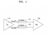
- FIG. 1 is a conceptual diagram of a high-speed interconnect system 100 according to various embodiments.
- the typical high-speed interconnect system 100 may include a transmitter 110, at least one channel (e.g., 121), and a receiver 130.
- the at least one channel includes a coaxial cable, a backplane, a printed circuit board (PCB), a package, or on-chip wires, and the length of the at least one channel (e.g., 121) may range from several centimeters to several tens of meters.
- the at least one channel (e.g., 121) has the characteristics of a low-pass filter (LPF). Accordingly, when a signal passes through the at least one channel (e.g., 121), intersymbol interference (ISI) may occur.
- LPF low-pass filter
- the ISI seriously hinders communication.
- the ISI is relatively small when the signal loss is 0 dB to 10 dB
- the ISI is large
- the ISI is large when the signal loss is 10 dB to 20 dB
- the ISI is significantly large when the signal loss is 20 dB to 30 dB.
- Embodiments described herein provide a method of limiting a transition level of a signal in order to prevent deterioration of signal quality due to ISI, while increasing the data rate.
- FIG. 2 is a block diagram illustrating a transmitting device 200 according to an embodiment.
- the transmitting device 200 may include a bit separator 210, an invalid-symbol detector 220, a frame buffer encoder 230, an input data encoder 240, and a communication unit 250.
- the bit separator 210, the invalid-symbol detector 220, the frame buffer encoder 230, the input data encoder 240, and the communication unit 250 may be modules included in respective programs to be executed by different processors or one processor. According to various embodiments, each component may be omitted or modified.
- the transmitting device 200 may correspond to the transmitter 110 in the high-speed interconnect system 100 described above with reference to FIG. 1 .
- the frame buffer encoder 230 and the input data encoder 240 may be configured in one processor.
- the processor may combine bits encoded by the frame buffer encoder 230 and the input data encoder 240 with each other, and transmit the combined bits to the communication unit 250.
- the bit separator 210 may separate symbols included in an input signal into a first bit, a second bit, and an n-th bit sequentially from the highest level, based on a specified criterion.
- the bit separator 210 may separate the first bit as a most significant bit (MSB), and separate the second bit and the n-th bit as a first least significant bit (LSB) and an n-1st LSB, respectively.
- MSB most significant bit
- LSB least significant bit
- n-1st LSB an n-1st LSB
- the bit separator 210 may group the bits included in the input signal into groups each including two bits. Then, the bit separator 210 may separate the first bit of the two bits in each group as an MSB, and separate the second bit as an LSB.
- bit separator 210 may group the bits included in the input signal into groups each including three bits. In addition, the bit separator 210 may separate the first bit of the three bits as an MSB, the second bit as a first LSB, and the third bit as a second LSB.
- the invalid-symbol detector 220 may identify, for example, a symbol of an input signal exceeding a specified transition level.
- the transition level may be specified by a user or a system, based on the state of a channel or system requirements.
- the transition level in PAM-4, the transition level may be specified as a value of 3 or less, and in PAM-8, the transition level may be specified as a value of 7 or less.
- the transition level is specified as 2 in PAM-4 and the transition level is specified as 5 in PAM-8.
- the invalid-symbol detector 220 may sequentially compare an (i-1)-th symbol with an i-th symbol, and check whether the i-th symbol exceeds the transition level. For example, when the difference between the (i-1)-th symbol and the i-th symbol in PAM-4 is '3', the invalid-symbol detector 220 may determine that the i-th symbol exceeds the specified transition level ('2'). As another example, when the difference between the (i-1)-th symbol and the i-th symbol in PAM-8 is '6' or '7', the invalid-symbol detector 220 may determines that the i-th symbol exceeds the specified transition level ('5').
- the invalid-symbol detector 220 may invert the MSB of the i-th symbol and again compare the i-th symbol with the (i-1)-th symbol. For example, in PAM-4, when the (i-1)-th symbol is '0' and the i-th symbol is '1', the invalid-symbol detector 220 having determined that the transition level is not exceeded may invert the MSB of the i-th symbol. The value of the i-th symbol whose MSB is inverted may be '3', and the invalid-symbol detector 220 may determine that the inverted i-th symbol exceeds the specified transition level ('2').
- the invalid-symbol detector 220 may invert the MSB only when the i-th symbol exceeds the specified transition level as a result of comparing the (i-1)-th symbol with the i-th symbol.
- the invalid-symbol detector 220 may determine that the i-th symbol is not inverted, when a result of comparing the (i-1)-th symbol with the i-th symbol whose MSB is inverted also exceeds the transition level.
- the invalid-symbol detector 220 may invert at least one of bits other than the MSB according to settings, when the i-th symbol exceeds the specified transition level, as a result of comparing the (i-1)-th symbol with the i-th symbol.
- the frame buffer encoder 230 may register at least one bit constituting the corresponding symbol, in a frame buffer.
- the frame buffer encoder 230 may register the MSB of the i-th symbol, in the frame buffer.
- the frame buffer encoder 230 may register '0' in the frame buffer when the MSB of the i-th symbol exceeding the specified transition level is '0', and may register '1' in the buffer frame when the MSB of the i-th symbol exceeding the specified transition level is '1'.
- the frame buffer encoder 230 may check whether a symbol obtained by combining a bit registered in the frame buffer with the LSB exceeds the specified transition level, and fill the frame buffer with a bit (i.e., a dummy bit) identical to the registered bit until the symbol obtained by combining the bit registered in the frame buffer with the LSB does not exceed the transition level.
- the frame buffer encoder 230 having registered '1' in the first bit of the frame buffer may continuously register '1' until the transition level of the symbol obtained by combining the second bit, which is the bit next to the first bit, with the LSB corresponding to the second bit does not exceed the specified level.
- the input data encoder 240 may encode input data by inverting at least one bit constituting a corresponding symbol.
- the input data encoder 240 may invert the MSB of the i-th symbol and then encode input data.
- the input data encoder 240 may invert the MSB to '1', and when the MSB of the i-th symbol exceeding the specified transition level is '1', the input data encoder 240 may invert the MSB to '0'.
- the input data encoder 240 does not invert at least one bit constituting the corresponding symbol.
- the input data encoder 240 encode the input data while maintaining the MSB of the i-th symbol.
- the communication unit 250 may combine the frame buffer encoded by the frame buffer encoder 230 with the input data encoded by the input data encoder 240, and transmit the resulting data to the receiver 130.
- the communication unit 250 may support establishment of a direct (e.g., wired) communication channel or a wireless communication channel between external electronic devices supporting PAM communication, and communication through the established communication channel.
- a direct (e.g., wired) communication channel or a wireless communication channel between external electronic devices supporting PAM communication, and communication through the established communication channel.
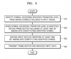
- FIG. 3 is a flowchart illustrating a method, performed by a transmitting device, of limiting a transition level and transmitting data, according to an embodiment.
- the transmitting device may identify a symbol exceeding a specified transition level, from among at least one symbol included in an input signal.
- the transmitting device may sequentially compare an (i-1)-th symbol with an i-th symbol included in the input signal, and based on a result of the comparing, identify whether the i-th symbol exceeds the specified transition level. For example, when the difference between a result of converting the (i-1)-th symbol into a decimal number and a result of converting the i-th symbol into a decimal number exceeds the specified transition level (e.g., 5), the transmitting device may identify the i-th symbol as a symbol exceeding the specified transition level.
- the specified transition level e.g., 5
- the transmitting device may obtain a frame buffer including at least one bit among bits constituting the identified symbol. For example, based on determining that the i-th symbol exceeds the specified transition level, the transmitting device may register the MSB of the i-th symbol, in the frame buffer.
- the transmitting device may encode input data by inverting at least one bit among the bits constituting the identified symbol. For example, based on determining that the i-th symbol exceeds the specified transition level, the transmitting device may encode a symbol obtained by inverting the MSB of the i-th symbol, as the input data.
- the transmitting device may transmit the frame buffer and the encoded input data.
- the transmitting device may combine the frame buffer with the encoded input data into one signal, and transmit the signal to a receiving device.
- the transmitting device may transmit the frame buffer and the encoded input data as separate signals, to the receiving device.
- FIG. 4 is a flowchart for describing in more detail a method, performed by a transmitting device, of limiting a transition level and transmitting data, according to an embodiment.
- the transmitting device may separate at least one symbol included in an input signal into bits.
- the transmitting device may separate the symbols included in the input signal into a first bit, a second bit, and an n-th bit, sequentially from the highest level based on a predetermined criterion.
- the transmitting device may separate the first bit as an MSB, and separate the second bit and the n-th bit as a first LSB and an n-1st LSB, respectively.
- the transmitting device may identify a symbol exceeding a specified transition level, from among the at least one symbol. For example, the transmitting device may sequentially compare an (i-1)-th symbol with an i-th symbol, and check whether the i-th symbol exceeds the transition level. After comparing the (i-1)-th symbol with the i-th symbol, the transmitting device according to an embodiment may invert the MSB of the i-th symbol and again compare the i-th symbol with the (i-1)-th symbol.
- the transmitting device may register at least one bit constituting the corresponding symbol, in a frame buffer.
- the transmitting device may sequentially register the MSB of the i-th symbol, in the frame buffer.
- the transmitting device may check whether the symbol combined with the LSB based on the frame buffer after the registering exceeds the specified transition level, and fill the frame buffer with a bit (i.e., a dummy bit) identical to the registered bit until the symbol does not exceed the transition level.
- the transmitting device may encode input data by inverting at least one bit constituting the corresponding symbol.
- the transmitting device may invert the MSB of the i-th symbol and then encode the input data.
- the transmitting device may combine the frame buffer with the encoded input data, and transmit the resulting data to a receiving device.
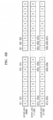
- FIGS. 5A and 5B are diagrams illustrating a method of limiting a transition level by using a PAM-4 data block, according to an embodiment.
- FIG. 5A illustrates an example of generating a data block by dividing symbols of an input signal into bits.
- a transmitting device may group bits included in the input signal into groups each including two bits. Then, the transmitting device may separate the first bit of the two bits in each group as an MSB, and separate the second bit as an LSB.
- the PAM-4 data block may include input data and frame buffer data.
- the frame buffer data may be written by allocating a part of a data block constituting the MSB, to a frame buffer data block 520.
- the length of the frame buffer data block 520 may be flexibly changed, and the length of an MSB input data block 510 may be determined based on the length of the frame buffer data block 520.
- FIGS. 5A and 5B illustrate a PAM-4 data block having a total length of 100.
- the length of the frame buffer data block 520 is set to 20
- the length of the MSB input data block 510 may be determined to be 80.
- the entire length of 100 may be used to allocate input data.
- a transmitting device may identify a symbol of an input signal exceeding a specified transition level. For example, the transmitting device may sequentially compare an (i-1)-th symbol with an i-th symbol, and check whether the i-th symbol exceeds the transition level.
- the first symbol has a value of '0' by combining a bit 511 with a bit 531.
- the second symbol has a symbol of '3' by combining a bit 512 with a bit 532, and the transmitting device may identify that the second symbol exceeds the specified transition level ('2'), by comparing the second symbol with the first symbol.
- a (k-1)-th symbol has a value of '0' by combining a bits 513 with a bit 533
- a k-th symbol has a value of '1' by combining a bit 514 with a bit 534.
- the transmitter 110 may determine again whether the specified transition level is exceeded, by inverting the bit 514, which is the MSB of the k-th symbol. In this case, by combining the inverted bit 514 with the bit 534, a value of '3' is obtained, and the transmitter 110 may determine that the k-th symbol exceeds the specified transition level ('2').
- FIG. 5B illustrates an example of encoding the MSB input data block 510 and the frame buffer data block 520.
- '1' which is an MSB 512 of the second symbol exceeding the specified transition level ('2')
- '2' may be registered in the frame buffer data block 520.
- FIG. 5B illustrates an example in which '1', which is the MSB 512 of the second symbol, is registered in a bit 521, which is the first bit of the frame buffer data block 520.
- the transmitting device may check whether the transition level of the frame buffer data block 520 is exceeded due to data registration. For example, the first symbol of the frame buffer data block 520 in which data is registered has a value of '3' by combining the bit 521 and a bit 535.
- the second symbol in which no data is registered has a symbol of '0' by combining a bit 522 with a bit 536, and the transmitting device may determine that the second symbol exceeds the specified transition level ('2'), by comparing the second symbol with the first symbol.
- the transmitting device may limit the transition level by registering '1', which is dummy data, in the second symbol of the frame buffer data block 520 as well.
- the transmitting device may continuously check whether the transition level of the frame buffer data block 520 is exceeded due to data registration. For example, the second symbol of the frame buffer data block 520 in which the dummy data is registered has a value of '2' by combining the bit 522 and a bit 536.
- the third symbol in which no data is registered has a symbol of '1' by combining a bit 523 with a bit 537, and satisfies the specified transition level.
- the transmitting device may invert the MSB of the third symbol, and determine again whether the transition level is exceeded.
- the transmitting device stops registering the dummy data.
- the transmitting device may encode the input data by inverting the MSB for which the data registration in the frame buffer data block 520 is completed.
- the specified transition level may be satisfied by inverting ('1' to '0') the bit 512 for which the data registration in the first bit 521 of the frame buffer data block 520 is completed.
- the transmitting device may register '0', which is an MSB 514 of the k-th symbol, in the third MSB 523 of the frame buffer data block 520.
- the transmitting device may check whether the transition level of the frame buffer data block 520 is exceeded due to data registration. However, because the k-th symbol already satisfies the specified transition level, the transmitting device does not invert the MSB 514 of the k-th symbol.
- FIGS. 6A and 6B are diagrams illustrating a method of limiting a transition level by using a PAM-8 data block, according to an embodiment.
- FIG. 6A illustrates an example of generating a data block by separating symbols of an input signal into bits.
- a transmitting device may group bits included in the input signal into groups each including three bits.
- the transmitting device may separate the first bit of the three bits in each group as an MSB, the second bit as a first LSB, and the third bit as a second LSB.
- the PAM-4 data block may include input data and frame buffer data.
- the frame buffer data may be written by allocating a part of a data block constituting the MSB, to a frame buffer data block 620.
- the length of the frame buffer data block 620 may be flexibly changed, and the length of an MSB input data block 610 may be determined based on the length of the frame buffer data block 620.
- FIGS. 6A and 6B illustrate a PAM-8 data block having a total length of 10000.
- the length of the frame buffer data block 620 is set to 2000
- the length of the MSB input data block 610 may be determined to be 8000.
- first and second LSB input data blocks 630 are not affected by the frame buffer data block 620, the entire length of 10000 may be used to allocate input data.
- the transmitting device may identify a symbol of an input signal exceeding a specified transition level.
- the transmitting device may sequentially compare an (i-1)-th symbol with an i-th symbol, and check whether the i-th symbol exceeds the transition level.
- the first symbol has a value of '0' by combining a bit 611, a bit 631a, and a bit 631b with each other.
- the second symbol has a symbol of '6' by combining a bit 612, a bit 632a, and a bit 632b with each other, and the transmitting device may determine that the second symbol exceeds the specified transition level ('5'), by comparing the second symbol with the first symbol.
- a (k-1)-th symbol may have a value of'1' by combining a bit 613, a bit 633a, and a bit 633b with each other
- a k-th symbol may have a value of '3' by combining a bit 614, a bit 634a, and a bit 634b with each other.
- the transmitting device may determine again whether the specified transition level is exceeded, by inverting the bit 614, which is the MSB of the k-th symbol.
- the k-th symbol has a value of '7' by combining the inverted bit 614, the bit 634a, and the bit 634b with each other, and the transmitting device may identify that the k-th symbol exceeds the specified transition level ('5').
- FIG. 6B illustrates an example of encoding the MSB input data block 610 and the frame buffer data block 620.
- '1' which is an MSB 612 of the second symbol exceeding the specified transition level ('5') may be registered in the frame buffer data block 620.
- FIG. 6B illustrates an example in which '1', which is the MSB 612 of the second symbol, is registered in a bit 621, which is the first bit of the frame buffer data block 620.
- the transmitting device may check whether the transition level of the frame buffer data block 620 is exceeded due to data registration. For example, the first symbol of the frame buffer data block 620 in which data is registered has a value of '7' by combining the bit 621, a bit 635a, and a bit 635b with each other.
- the second symbol in which no data is registered has a symbol of'1' obtained by combining a bit 622, a bit 636a, and a bit 636b with each other, and the transmitting device may determine that the second symbol exceeds the specified transition level ('5'), by comparing the second symbol with the first symbol.
- the transmitting device may limit the transition level by registering '1', which is dummy data, in the second symbol of the frame buffer data block 620 as well.
- the transmitting device may continuously check whether the transition level of the frame buffer data block 620 is exceeded due to data registration.
- the second symbol of the frame buffer data block 620 in which the dummy data is registered has a value of '5' by combining the bit 622, the bit 636a, and the bit 636b with each other.
- the third symbol in which no data is registered has a symbol of '2' by combining a bit 623, a bit 637a, and a bit 637b with each other, and satisfies the specified transition level.
- the transmitting device may invert the MSB of the third symbol, and determine again whether the transition level is exceeded based on the inverted MSB. For example, the transmitting device determines that the second symbol has a value of '6' by combining the inverted bit 623, the bit 637a, and the bit 637b with each other, and thus satisfies the specified transition level, and stops registering the dummy data.
- the transmitting device may encode the input data by inverting the MSB for which the data registration in the frame buffer data block 620 is completed.
- the specified transition level may be satisfied by inverting ('1' to '0') the bit 612 for which data registration in the bit 621 is completed.
- the transmitting device may register '0', which is an MSB 614 of the k-th symbol, in a third MSB 623 of the frame buffer data block 620.
- the transmitting device may check whether the transition level of the frame buffer data block 620 is exceeded due to data registration. However, because the k-th symbol already satisfies the specified transition level, the transmitting device does not invert the MSB 614 of the k-th symbol.
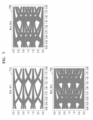
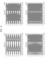
- FIG. 7 is an eye-diagram in a case in which a transition level is limited in PAM-4 communication, according to an embodiment.
- a first eye-diagram 710 of FIG. 7 shows a case in which a transition level limit is set to 1 in PAM-4 communication having a total of 4 levels.
- the transition level limit is specified as 1 in PAM-4 communication
- the bit error ratio becomes almost zero because the eye-opening is significantly large.
- the data rate may become significantly low.
- a second eye-diagram 720 of FIG. 7 shows a case in which a transition level limit is set to 2 in PAM-4 communication having a total of 4 levels.
- a practical communication environment with relatively large eye-opening and significantly little bit error ratio may be provided.
- a third eye-diagram 730 of FIG. 7 shows a case in which a transition level limit is set to 3 in PAM-4 communication having a total of 4 levels. Specifying the transition level limit as 3 in PAM-4 communication practically corresponds to a case in which there is substantially no transition level limit, and the bit error ratio may become significantly high depending on the channel environment.
- FIG. 8 is an eye-diagram in a case in which a transition level is limited in PAM-8 communication, according to an embodiment.
- a first eye-diagram 810 of FIG. 8 shows a case in which a transition level limit is set to 1 in PAM-8 communication having a total of 8 levels.
- the transition level limit is specified as 1 in PAM-8 communication
- the bit error ratio is significantly low because the eye-opening is significantly large.
- the data rate becomes significantly low.
- a second eye-diagram 820 of FIG. 8 shows a case in which a transition level limit is set to 3 in PAM-8 communication having a total of 8 levels.
- a practical communication environment with relatively large eye-opening and significantly little bit error ratio may be provided.
- a third eye-diagram 830 of FIG. 8 shows a case in which a transition level limit is set to 4 in PAM-8 communication having a total of 8 levels.
- a practical communication environment with relatively large eye-opening and significantly little bit error ratio may be provided.
- a fourth eye-diagram 840 of FIG. 8 shows a case in which a transition level limit is set to 7 in PAM-8 communication having a total of 8 levels. Specifying the transition level limit as 7 in PAM-8 communication corresponds to a case in which there is substantially no transition level limit, and the bit error ratio may become significantly high depending on the channel environment.
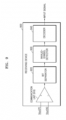
- FIG. 9 is a block diagram illustrating a receiving device 900 according to an embodiment.
- the receiving device 900 may include a communication unit 910, a bit separator 920, an invalid-symbol detector 930, and a decoder 940.
- the communication unit 910, the bit separator 920, the invalid-symbol detector 930, and the decoder 940 may be modules included in respective programs to be executed by different processors or one processor. According to various embodiments, each component may be omitted or modified.
- the receiving device 900 may correspond to the receiver 130 in the high-speed interconnect system 100 described above with reference to FIG. 1 .
- the communication unit 910 may receive data transmitted from a transmitting device.
- the communication unit 910 may support establishment of a direct (e.g., wired) communication channel or a wireless communication channel between external electronic devices supporting PAM communication, and communication through the established communication channel.
- the bit separator 920 may separate symbols included in an input signal into a first bit, a second bit, and an n-th bit sequentially from the highest level, based on a specified criterion.
- the bit separator 920 may separate the first bit as an MSB, and separate the second bit and the n-th bit as a first LSB and an n-1st LSB, respectively.
- the invalid-symbol detector 930 may identify, for example, a symbol of an input signal exceeding a specified transition level.
- the transition level may be specified by a user or a system, based on the state of a channel.
- the transition level in PAM-4, the transition level may be specified as a value of 3 or less, and in PAM-8, the transition level may be specified as a value of 7 or less.
- the transition level is specified as 2 in PAM-4 and the transition level is specified as 5 in PAM-8.
- the invalid-symbol detector 930 may sequentially compare an (i-1)-th symbol with an i-th symbol, and check whether the i-th symbol exceeds the transition level. For example, when the difference between the (i-1)-th symbol and the i-th symbol in PAM-4 is '3', the invalid-symbol detector 930 may determines that the i-th symbol exceeds the specified transition level ('2'). As another example, when the difference between the (i-1)-th symbol and the i-th symbol in PAM-8 is '6' or '7', the invalid-symbol detector 930 may determines that the i-th symbol exceeds the specified transition level ('5').
- the invalid-symbol detector 930 may invert the MSB of the i-th symbol and again compare the i-th symbol with the (i-1)-th symbol.
- the invalid-symbol detector 930 when the (i-1)-th symbol is '0' and the i-th symbol is '1', the invalid-symbol detector 930 having determined that the transition level is not exceeded may invert the MSB of the i-th symbol.
- the value of the i-th symbol whose MSB is inverted may be '3', and the invalid-symbol detector 930 may determine that the i-th symbol exceeds the specified transition level ('2').
- the decoder 940 may restore the input data based on data registered in the frame buffer.
- the decoder 940 may extract at least one bit registered in the frame buffer, and restore the corresponding symbol based on the extracted at least one bit. For example, based on determining that the i-th symbol exceeds the specified transition level, the decoder 940 may restore the MSB of the i-th symbol based on the bit registered in the frame buffer.
- the decoder 940 may restore the MSB of the i-th symbol, as '0'.
- the decoder 940 may restore the MSB of the i-th symbol, as '1'.
- FIG. 10 is a flowchart illustrating a method, performed by a receiving device, of limiting a transition level and receiving data, according to an embodiment.
- the receiving device may receive data from a transmitting device.
- the receiving device may receive, from the transmitting device, data in which a frame buffer and encoded input data are combined with each other.
- the receiving device may separate symbols of the input signal into bits. For example, the receiving device may separate the symbols included in the input signal into a first bit, a second bit, and an n-th bit, sequentially from the highest level based on a predetermined criterion. For example, the receiving device may separate the first bit as an MSB, and separate the second bit and the n-th bit as a first LSB and an n-1st LSB, respectively.
- the receiving device may identify a symbol exceeding a specified transition level, from among the symbols of the input signal. For example, the receiving device may sequentially compare an (i-1)-th symbol with an i-th symbol, and check whether the i-th symbol exceeds the transition level. After comparing the (i-1)-th symbol with the i-th symbol, the receiving device according to an embodiment may invert the MSB of the i-th symbol and again compare the i-th symbol with the (i-1)-th symbol.
- the receiving device may restore the input data based on data registered in the frame buffer. For example, when a symbol exceeding the transition level is detected, the receiving device may extract at least one bit registered in the frame buffer, and restore the corresponding symbol. For example, based on determining that the i-th symbol exceeds the specified transition level, the receiving device may restore the MSB of the i-th symbol based on the bit registered in the frame buffer.
- the PAM transmitter and receiver according to an embodiment have an effect of providing PAM communication with a high data rate and a low data error rate, and are able to adaptively set a limit level without applying an additional digital circuit.
- the device described above may be implemented as a hardware component, a software component, and/or a combination of a hardware component and a software component.
- the devices and components described in the embodiments may be implemented by using one or more general-purpose computers or special-purpose computers, such as a processor, a controller, an arithmetic logic unit (ALU), a digital signal processor, a microcomputer, a field-programmable gate array (FPGA), a programmable logic unit (PLU), a microprocessor, or any other device configured to execute and respond to instructions.
- the processor may execute an operating system (OS) and one or more software applications running on the OS.
- the processor may also access, store, modify, process, and generate information in response to execution of software.
- OS operating system
- the processor may also access, store, modify, process, and generate information in response to execution of software.
- processors may include a plurality of processing elements and/or a plurality of types of processing elements.
- the processor may include one or more processors and one controller.
- other processing configurations are also possible, such as a parallel processor.
- the software may include a computer program, code, instructions, or a combination of one or more thereof, and may configure the processor to operate as desired or may independently or collectively instruct the processor.
- Software and/or information may be embodied permanently or temporarily in any type of machine, component, physical or virtual equipment, computer storage medium, or device, for providing instructions or information to or being interpreted by the processor.
- Software may be distributed on networked computer systems and stored or executed in a distributed manner.
- the software and information may be stored in one or more computer-readable recording media.
- the method according to an embodiment may be embodied as program commands executable by various computer devices, and recorded on a computer-readable medium.
- the computer-readable recording medium include magnetic media such as hard disks, floppy disks, or magnetic tapes, optical media such as compact disc ROMs (CD-ROMs) or digital video discs (DVDs), magneto-optical media such as floptical disks, and hardware devices such as ROM, RAM, and flash memory, which are specially configured to store and execute program instructions.
- Examples of the program instructions include not only machine code, such as code made by a compiler, but also high-level language code that is executable by a computer by using an interpreter or the like.
- the PAM transmitter and receiver according to an embodiment are able to perform PAM communication with a high data rate and a low data error rate, and adaptively set a limit level without applying an additional digital circuit.
Landscapes
- Engineering & Computer Science (AREA)
- Computer Networks & Wireless Communication (AREA)
- Signal Processing (AREA)
- Physics & Mathematics (AREA)
- Spectroscopy & Molecular Physics (AREA)
- Dc Digital Transmission (AREA)
Applications Claiming Priority (2)
| Application Number | Priority Date | Filing Date | Title |
|---|---|---|---|
| KR20220048694 | 2022-04-20 | ||
| KR1020230043086A KR102717159B1 (ko) | 2022-04-20 | 2023-03-31 | 펄스 진폭 변조 송신기/수신기 및 이의 트랜지션 레벨을 제한하는 방법 |
Publications (1)
| Publication Number | Publication Date |
|---|---|
| EP4266636A1 true EP4266636A1 (fr) | 2023-10-25 |
Family
ID=86052228
Family Applications (1)
| Application Number | Title | Priority Date | Filing Date |
|---|---|---|---|
| EP23167959.8A Pending EP4266636A1 (fr) | 2022-04-20 | 2023-04-14 | Emetteur et récepteur à modulation d'amplitude d'impulsion et procédé de limitation de niveau de transition associé |
Country Status (2)
| Country | Link |
|---|---|
| US (1) | US12170586B2 (fr) |
| EP (1) | EP4266636A1 (fr) |
Citations (1)
| Publication number | Priority date | Publication date | Assignee | Title |
|---|---|---|---|---|
| WO2016007221A1 (fr) * | 2014-07-10 | 2016-01-14 | Qualcomm Incorporated | Technique de réduction de puissance de liaison pour la transmission de données à l'aide de modulation d'amplitude d'impulsion bipolaire |
Family Cites Families (15)
| Publication number | Priority date | Publication date | Assignee | Title |
|---|---|---|---|---|
| US7397848B2 (en) | 2003-04-09 | 2008-07-08 | Rambus Inc. | Partial response receiver |
| US7876866B1 (en) | 2005-01-27 | 2011-01-25 | Pmc-Sierra Us, Inc. | Data subset selection algorithm for reducing data-pattern autocorrelations |
| KR100674953B1 (ko) | 2005-02-05 | 2007-01-26 | 학교법인 포항공과대학교 | 반도체 메모리의 등화 수신기 |
| JP2011015071A (ja) * | 2009-06-30 | 2011-01-20 | Sony Corp | 信号処理装置、情報処理装置、多値符号化方法、及びデータ伝送方法 |
| US9172567B2 (en) | 2013-11-25 | 2015-10-27 | Qualcomm Incorporated | Methods and apparatus to reduce signaling power |
| US9674025B2 (en) * | 2014-07-01 | 2017-06-06 | International Business Machines Corporation | 4-level pulse amplitude modulation transmitter architectures utilizing quadrature clock phases |
| KR20170008077A (ko) * | 2015-07-13 | 2017-01-23 | 에스케이하이닉스 주식회사 | 고속 통신을 위한 인터페이스 회로 및 이를 포함하는 시스템 |
| US10142089B2 (en) * | 2017-03-22 | 2018-11-27 | Oracle International Corporation | Baud-rate clock data recovery with improved tracking performance |
| US10205525B1 (en) * | 2017-11-30 | 2019-02-12 | International Business Machines Corporation | PAM-4 transmitter precoder for 1+0.5D PR channels |
| US11966348B2 (en) * | 2019-01-28 | 2024-04-23 | Nvidia Corp. | Reducing coupling and power noise on PAM-4 I/O interface |
| US10547387B2 (en) * | 2018-03-30 | 2020-01-28 | Mellanox Technologies Denmark ApS. | Transition based feedforward equalization method and apparatus implemented with lookup table circuits |
| US11405248B2 (en) * | 2020-02-21 | 2022-08-02 | Prodigy Technovations Pvt. Ltd. | FPGA based system for decoding PAM-3 signals |
| KR102855061B1 (ko) | 2020-09-02 | 2025-09-04 | 삼성전자주식회사 | 멀티 레벨 신호 수신기 및 이를 포함하는 메모리 시스템 |
| EP4057516B1 (fr) | 2021-03-10 | 2024-03-27 | Samsung Electronics Co., Ltd. | Appareils de codage pour la mise en oeuvre d'un codage multimode |
| KR20220127129A (ko) | 2021-03-10 | 2022-09-19 | 삼성전자주식회사 | 멀티 모드 코딩을 구현하는 인코딩 및 디코딩 장치 및 방법 |
-
2023
- 2023-04-14 EP EP23167959.8A patent/EP4266636A1/fr active Pending
- 2023-04-18 US US18/302,392 patent/US12170586B2/en active Active
Patent Citations (1)
| Publication number | Priority date | Publication date | Assignee | Title |
|---|---|---|---|---|
| WO2016007221A1 (fr) * | 2014-07-10 | 2016-01-14 | Qualcomm Incorporated | Technique de réduction de puissance de liaison pour la transmission de données à l'aide de modulation d'amplitude d'impulsion bipolaire |
Also Published As
| Publication number | Publication date |
|---|---|
| US12170586B2 (en) | 2024-12-17 |
| US20230344686A1 (en) | 2023-10-26 |
Similar Documents
| Publication | Publication Date | Title |
|---|---|---|
| US9220023B2 (en) | Methods for signaling a maximum number of MSDUs in a transmission | |
| US9246713B2 (en) | Vector signaling with reduced receiver complexity | |
| US9504042B2 (en) | System and method for encoding and decoding of data with channel polarization mechanism | |
| US20150067380A1 (en) | Power control method and apparatus | |
| US10051489B2 (en) | Method of CSI reporting, user equipment and enode B | |
| US11444639B2 (en) | Method and system for polar code coding | |
| CN113168393A (zh) | 高速的硬件传输均衡 | |
| WO2017168255A1 (fr) | Procédé et appareil pour déterminer des informations de canal | |
| RU2733809C1 (ru) | Способ и устройство для отладки параметра соединения serdes и компьютерный носитель данных | |
| KR20160021264A (ko) | 통신 방법 및 장치 | |
| US9813111B2 (en) | Phantom mode datastream transmission | |
| EP4266636A1 (fr) | Emetteur et récepteur à modulation d'amplitude d'impulsion et procédé de limitation de niveau de transition associé | |
| WO2021022874A1 (fr) | Procédé, appareil, et dispositif de traitement de capacité de terminal | |
| WO2023077871A1 (fr) | Procédé d'indication, procédé d'envoi de signal de référence, nœud de communication et support de stockage | |
| US20150244620A1 (en) | Method and apparatus for aggregating and encoding received symbols including generation of a pointer for a control code | |
| US7302631B2 (en) | Low overhead coding techniques | |
| KR102717159B1 (ko) | 펄스 진폭 변조 송신기/수신기 및 이의 트랜지션 레벨을 제한하는 방법 | |
| CN110224731A (zh) | 一种码本子集限制的方法 | |
| CN116915556A (zh) | 脉冲幅度调制发送器和接收器及限制其转变电平的方法 | |
| US10651997B2 (en) | Pilot signal configuration method and device | |
| KR102254337B1 (ko) | Dc-밸런싱을 고려한 pam4 5b3q 코딩 방법 및 장치 | |
| CN111342858B (zh) | 信号处理方法及装置 | |
| US8165176B1 (en) | System and method for generating a frequency rich spectrum in a data stream | |
| US20140362932A1 (en) | Communication apparatus, communication system, communication method, and storage medium | |
| JP7823495B2 (ja) | 受信装置、受信方法、受信プログラム及び送信装置 |
Legal Events
| Date | Code | Title | Description |
|---|---|---|---|
| STAA | Information on the status of an ep patent application or granted ep patent |
Free format text: STATUS: REQUEST FOR EXAMINATION WAS MADE |
|
| PUAI | Public reference made under article 153(3) epc to a published international application that has entered the european phase |
Free format text: ORIGINAL CODE: 0009012 |
|
| 17P | Request for examination filed |
Effective date: 20230414 |
|
| AK | Designated contracting states |
Kind code of ref document: A1 Designated state(s): AL AT BE BG CH CY CZ DE DK EE ES FI FR GB GR HR HU IE IS IT LI LT LU LV MC ME MK MT NL NO PL PT RO RS SE SI SK SM TR |
|
| STAA | Information on the status of an ep patent application or granted ep patent |
Free format text: STATUS: EXAMINATION IS IN PROGRESS |
|
| 17Q | First examination report despatched |
Effective date: 20251024 |