EP4266661A1 - Capteur de ligne optique - Google Patents
Capteur de ligne optique Download PDFInfo
- Publication number
- EP4266661A1 EP4266661A1 EP21906100.9A EP21906100A EP4266661A1 EP 4266661 A1 EP4266661 A1 EP 4266661A1 EP 21906100 A EP21906100 A EP 21906100A EP 4266661 A1 EP4266661 A1 EP 4266661A1
- Authority
- EP
- European Patent Office
- Prior art keywords
- light receiving
- lens
- lenses
- line sensor
- sensor according
- Prior art date
- Legal status (The legal status is an assumption and is not a legal conclusion. Google has not performed a legal analysis and makes no representation as to the accuracy of the status listed.)
- Pending
Links
Images














Classifications
-
- G—PHYSICS
- G02—OPTICS
- G02B—OPTICAL ELEMENTS, SYSTEMS OR APPARATUS
- G02B26/00—Optical devices or arrangements for the control of light using movable or deformable optical elements
- G02B26/08—Optical devices or arrangements for the control of light using movable or deformable optical elements for controlling the direction of light
- G02B26/10—Scanning systems
- G02B26/12—Scanning systems using multifaceted mirrors
- G02B26/125—Details of the optical system between the polygonal mirror and the image plane
-
- G—PHYSICS
- G02—OPTICS
- G02B—OPTICAL ELEMENTS, SYSTEMS OR APPARATUS
- G02B3/00—Simple or compound lenses
- G02B3/0006—Arrays
- G02B3/0037—Arrays characterized by the distribution or form of lenses
- G02B3/005—Arrays characterized by the distribution or form of lenses arranged along a single direction only, e.g. lenticular sheets
-
- G—PHYSICS
- G01—MEASURING; TESTING
- G01N—INVESTIGATING OR ANALYSING MATERIALS BY DETERMINING THEIR CHEMICAL OR PHYSICAL PROPERTIES
- G01N21/00—Investigating or analysing materials by the use of optical means, i.e. using sub-millimetre waves, infrared, visible or ultraviolet light
- G01N21/84—Systems specially adapted for particular applications
- G01N21/88—Investigating the presence of flaws or contamination
- G01N21/8806—Specially adapted optical and illumination features
-
- G—PHYSICS
- G01—MEASURING; TESTING
- G01N—INVESTIGATING OR ANALYSING MATERIALS BY DETERMINING THEIR CHEMICAL OR PHYSICAL PROPERTIES
- G01N21/00—Investigating or analysing materials by the use of optical means, i.e. using sub-millimetre waves, infrared, visible or ultraviolet light
- G01N21/84—Systems specially adapted for particular applications
- G01N21/88—Investigating the presence of flaws or contamination
- G01N21/8851—Scan or image signal processing specially adapted therefor, e.g. for scan signal adjustment, for detecting different kinds of defects, for compensating for structures, markings, edges
-
- G—PHYSICS
- G01—MEASURING; TESTING
- G01N—INVESTIGATING OR ANALYSING MATERIALS BY DETERMINING THEIR CHEMICAL OR PHYSICAL PROPERTIES
- G01N21/00—Investigating or analysing materials by the use of optical means, i.e. using sub-millimetre waves, infrared, visible or ultraviolet light
- G01N21/84—Systems specially adapted for particular applications
- G01N21/88—Investigating the presence of flaws or contamination
- G01N21/89—Investigating the presence of flaws or contamination in moving material, e.g. running paper or textiles
- G01N21/8901—Optical details; Scanning details
-
- G—PHYSICS
- G02—OPTICS
- G02B—OPTICAL ELEMENTS, SYSTEMS OR APPARATUS
- G02B26/00—Optical devices or arrangements for the control of light using movable or deformable optical elements
- G02B26/08—Optical devices or arrangements for the control of light using movable or deformable optical elements for controlling the direction of light
- G02B26/10—Scanning systems
- G02B26/12—Scanning systems using multifaceted mirrors
- G02B26/123—Multibeam scanners, e.g. using multiple light sources or beam splitters
-
- G—PHYSICS
- G02—OPTICS
- G02B—OPTICAL ELEMENTS, SYSTEMS OR APPARATUS
- G02B3/00—Simple or compound lenses
- G02B3/0006—Arrays
-
- G—PHYSICS
- G07—CHECKING-DEVICES
- G07D—HANDLING OF COINS OR VALUABLE PAPERS, e.g. TESTING, SORTING BY DENOMINATIONS, COUNTING, DISPENSING, CHANGING OR DEPOSITING
- G07D7/00—Testing specially adapted to determine the identity or genuineness of valuable papers or for segregating those which are unacceptable, e.g. banknotes that are alien to a currency
- G07D7/06—Testing specially adapted to determine the identity or genuineness of valuable papers or for segregating those which are unacceptable, e.g. banknotes that are alien to a currency using wave or particle radiation
- G07D7/12—Visible light, infrared or ultraviolet radiation
-
- G—PHYSICS
- G07—CHECKING-DEVICES
- G07D—HANDLING OF COINS OR VALUABLE PAPERS, e.g. TESTING, SORTING BY DENOMINATIONS, COUNTING, DISPENSING, CHANGING OR DEPOSITING
- G07D7/00—Testing specially adapted to determine the identity or genuineness of valuable papers or for segregating those which are unacceptable, e.g. banknotes that are alien to a currency
- G07D7/06—Testing specially adapted to determine the identity or genuineness of valuable papers or for segregating those which are unacceptable, e.g. banknotes that are alien to a currency using wave or particle radiation
- G07D7/12—Visible light, infrared or ultraviolet radiation
- G07D7/121—Apparatus characterised by sensor details
-
- H—ELECTRICITY
- H04—ELECTRIC COMMUNICATION TECHNIQUE
- H04N—PICTORIAL COMMUNICATION, e.g. TELEVISION
- H04N1/00—Scanning, transmission or reproduction of documents or the like, e.g. facsimile transmission; Details thereof
- H04N1/024—Details of scanning heads ; Means for illuminating the original
- H04N1/02409—Focusing, i.e. adjusting the focus of the scanning head
-
- H—ELECTRICITY
- H04—ELECTRIC COMMUNICATION TECHNIQUE
- H04N—PICTORIAL COMMUNICATION, e.g. TELEVISION
- H04N1/00—Scanning, transmission or reproduction of documents or the like, e.g. facsimile transmission; Details thereof
- H04N1/024—Details of scanning heads ; Means for illuminating the original
- H04N1/02481—Arrangements for positioning elements within a head
-
- H—ELECTRICITY
- H04—ELECTRIC COMMUNICATION TECHNIQUE
- H04N—PICTORIAL COMMUNICATION, e.g. TELEVISION
- H04N1/00—Scanning, transmission or reproduction of documents or the like, e.g. facsimile transmission; Details thereof
- H04N1/024—Details of scanning heads ; Means for illuminating the original
- H04N1/0249—Arrangements for mounting or supporting elements within a scanning head
-
- H—ELECTRICITY
- H04—ELECTRIC COMMUNICATION TECHNIQUE
- H04N—PICTORIAL COMMUNICATION, e.g. TELEVISION
- H04N1/00—Scanning, transmission or reproduction of documents or the like, e.g. facsimile transmission; Details thereof
- H04N1/024—Details of scanning heads ; Means for illuminating the original
- H04N1/028—Details of scanning heads ; Means for illuminating the original for picture information pick-up
- H04N1/02815—Means for illuminating the original, not specific to a particular type of pick-up head
- H04N1/0282—Using a single or a few point light sources, e.g. a laser diode
-
- H—ELECTRICITY
- H04—ELECTRIC COMMUNICATION TECHNIQUE
- H04N—PICTORIAL COMMUNICATION, e.g. TELEVISION
- H04N1/00—Scanning, transmission or reproduction of documents or the like, e.g. facsimile transmission; Details thereof
- H04N1/024—Details of scanning heads ; Means for illuminating the original
- H04N1/028—Details of scanning heads ; Means for illuminating the original for picture information pick-up
- H04N1/02815—Means for illuminating the original, not specific to a particular type of pick-up head
- H04N1/02845—Means for illuminating the original, not specific to a particular type of pick-up head using an elongated light source, e.g. tubular lamp, LED array
- H04N1/0286—Means for illuminating the original, not specific to a particular type of pick-up head using an elongated light source, e.g. tubular lamp, LED array in combination with a light integrating, concentrating or defusing cavity
-
- H—ELECTRICITY
- H04—ELECTRIC COMMUNICATION TECHNIQUE
- H04N—PICTORIAL COMMUNICATION, e.g. TELEVISION
- H04N1/00—Scanning, transmission or reproduction of documents or the like, e.g. facsimile transmission; Details thereof
- H04N1/024—Details of scanning heads ; Means for illuminating the original
- H04N1/028—Details of scanning heads ; Means for illuminating the original for picture information pick-up
- H04N1/02815—Means for illuminating the original, not specific to a particular type of pick-up head
- H04N1/02845—Means for illuminating the original, not specific to a particular type of pick-up head using an elongated light source, e.g. tubular lamp, LED array
- H04N1/02865—Means for illuminating the original, not specific to a particular type of pick-up head using an elongated light source, e.g. tubular lamp, LED array using an array of light sources or a combination of such arrays, e.g. an LED bar
-
- H—ELECTRICITY
- H04—ELECTRIC COMMUNICATION TECHNIQUE
- H04N—PICTORIAL COMMUNICATION, e.g. TELEVISION
- H04N1/00—Scanning, transmission or reproduction of documents or the like, e.g. facsimile transmission; Details thereof
- H04N1/024—Details of scanning heads ; Means for illuminating the original
- H04N1/028—Details of scanning heads ; Means for illuminating the original for picture information pick-up
- H04N1/03—Details of scanning heads ; Means for illuminating the original for picture information pick-up with photodetectors arranged in a substantially linear array
-
- H—ELECTRICITY
- H04—ELECTRIC COMMUNICATION TECHNIQUE
- H04N—PICTORIAL COMMUNICATION, e.g. TELEVISION
- H04N1/00—Scanning, transmission or reproduction of documents or the like, e.g. facsimile transmission; Details thereof
- H04N1/024—Details of scanning heads ; Means for illuminating the original
- H04N1/028—Details of scanning heads ; Means for illuminating the original for picture information pick-up
- H04N1/03—Details of scanning heads ; Means for illuminating the original for picture information pick-up with photodetectors arranged in a substantially linear array
- H04N1/031—Details of scanning heads ; Means for illuminating the original for picture information pick-up with photodetectors arranged in a substantially linear array the photodetectors having a one-to-one and optically positive correspondence with the scanned picture elements, e.g. linear contact sensors
-
- H—ELECTRICITY
- H04—ELECTRIC COMMUNICATION TECHNIQUE
- H04N—PICTORIAL COMMUNICATION, e.g. TELEVISION
- H04N1/00—Scanning, transmission or reproduction of documents or the like, e.g. facsimile transmission; Details thereof
- H04N1/024—Details of scanning heads ; Means for illuminating the original
- H04N1/028—Details of scanning heads ; Means for illuminating the original for picture information pick-up
- H04N1/03—Details of scanning heads ; Means for illuminating the original for picture information pick-up with photodetectors arranged in a substantially linear array
- H04N1/031—Details of scanning heads ; Means for illuminating the original for picture information pick-up with photodetectors arranged in a substantially linear array the photodetectors having a one-to-one and optically positive correspondence with the scanned picture elements, e.g. linear contact sensors
- H04N1/0311—Details of scanning heads ; Means for illuminating the original for picture information pick-up with photodetectors arranged in a substantially linear array the photodetectors having a one-to-one and optically positive correspondence with the scanned picture elements, e.g. linear contact sensors using an array of elements to project the scanned image elements onto the photodetectors
-
- H—ELECTRICITY
- H04—ELECTRIC COMMUNICATION TECHNIQUE
- H04N—PICTORIAL COMMUNICATION, e.g. TELEVISION
- H04N1/00—Scanning, transmission or reproduction of documents or the like, e.g. facsimile transmission; Details thereof
- H04N1/024—Details of scanning heads ; Means for illuminating the original
- H04N1/028—Details of scanning heads ; Means for illuminating the original for picture information pick-up
- H04N1/03—Details of scanning heads ; Means for illuminating the original for picture information pick-up with photodetectors arranged in a substantially linear array
- H04N1/031—Details of scanning heads ; Means for illuminating the original for picture information pick-up with photodetectors arranged in a substantially linear array the photodetectors having a one-to-one and optically positive correspondence with the scanned picture elements, e.g. linear contact sensors
- H04N1/0311—Details of scanning heads ; Means for illuminating the original for picture information pick-up with photodetectors arranged in a substantially linear array the photodetectors having a one-to-one and optically positive correspondence with the scanned picture elements, e.g. linear contact sensors using an array of elements to project the scanned image elements onto the photodetectors
- H04N1/0312—Details of scanning heads ; Means for illuminating the original for picture information pick-up with photodetectors arranged in a substantially linear array the photodetectors having a one-to-one and optically positive correspondence with the scanned picture elements, e.g. linear contact sensors using an array of elements to project the scanned image elements onto the photodetectors using an array of optical fibres or rod-lenses
-
- H—ELECTRICITY
- H04—ELECTRIC COMMUNICATION TECHNIQUE
- H04N—PICTORIAL COMMUNICATION, e.g. TELEVISION
- H04N1/00—Scanning, transmission or reproduction of documents or the like, e.g. facsimile transmission; Details thereof
- H04N1/024—Details of scanning heads ; Means for illuminating the original
- H04N1/028—Details of scanning heads ; Means for illuminating the original for picture information pick-up
- H04N1/03—Details of scanning heads ; Means for illuminating the original for picture information pick-up with photodetectors arranged in a substantially linear array
- H04N1/031—Details of scanning heads ; Means for illuminating the original for picture information pick-up with photodetectors arranged in a substantially linear array the photodetectors having a one-to-one and optically positive correspondence with the scanned picture elements, e.g. linear contact sensors
- H04N1/0318—Integral pick-up heads, i.e. self-contained heads whose basic elements are a light-source, a lens array and a photodetector array which are supported by a single-piece frame
-
- H—ELECTRICITY
- H04—ELECTRIC COMMUNICATION TECHNIQUE
- H04N—PICTORIAL COMMUNICATION, e.g. TELEVISION
- H04N1/00—Scanning, transmission or reproduction of documents or the like, e.g. facsimile transmission; Details thereof
- H04N1/04—Scanning arrangements, i.e. arrangements for the displacement of active reading or reproducing elements relative to the original or reproducing medium, or vice versa
- H04N1/19—Scanning arrangements, i.e. arrangements for the displacement of active reading or reproducing elements relative to the original or reproducing medium, or vice versa using multi-element arrays
- H04N1/191—Scanning arrangements, i.e. arrangements for the displacement of active reading or reproducing elements relative to the original or reproducing medium, or vice versa using multi-element arrays the array comprising a one-dimensional [1D] array
-
- G—PHYSICS
- G01—MEASURING; TESTING
- G01N—INVESTIGATING OR ANALYSING MATERIALS BY DETERMINING THEIR CHEMICAL OR PHYSICAL PROPERTIES
- G01N21/00—Investigating or analysing materials by the use of optical means, i.e. using sub-millimetre waves, infrared, visible or ultraviolet light
- G01N21/84—Systems specially adapted for particular applications
- G01N21/88—Investigating the presence of flaws or contamination
- G01N21/8806—Specially adapted optical and illumination features
- G01N2021/8812—Diffuse illumination, e.g. "sky"
- G01N2021/8816—Diffuse illumination, e.g. "sky" by using multiple sources, e.g. LEDs
-
- G—PHYSICS
- G01—MEASURING; TESTING
- G01N—INVESTIGATING OR ANALYSING MATERIALS BY DETERMINING THEIR CHEMICAL OR PHYSICAL PROPERTIES
- G01N21/00—Investigating or analysing materials by the use of optical means, i.e. using sub-millimetre waves, infrared, visible or ultraviolet light
- G01N21/84—Systems specially adapted for particular applications
- G01N21/88—Investigating the presence of flaws or contamination
- G01N21/8806—Specially adapted optical and illumination features
- G01N2021/8845—Multiple wavelengths of illumination or detection
-
- G—PHYSICS
- G01—MEASURING; TESTING
- G01N—INVESTIGATING OR ANALYSING MATERIALS BY DETERMINING THEIR CHEMICAL OR PHYSICAL PROPERTIES
- G01N21/00—Investigating or analysing materials by the use of optical means, i.e. using sub-millimetre waves, infrared, visible or ultraviolet light
- G01N21/84—Systems specially adapted for particular applications
- G01N21/88—Investigating the presence of flaws or contamination
- G01N21/8851—Scan or image signal processing specially adapted therefor, e.g. for scan signal adjustment, for detecting different kinds of defects, for compensating for structures, markings, edges
- G01N2021/8887—Scan or image signal processing specially adapted therefor, e.g. for scan signal adjustment, for detecting different kinds of defects, for compensating for structures, markings, edges based on image processing techniques
Definitions
- the present invention relates to an optical line sensor that mainly detects a scratch and a defect on a surface of a thin inspection object such as a printed matter or a film and a scratch and a defect inside a transparent film.
- CIS contact-type optical sensor
- CIS contact-type optical sensor
- an inspection machine for discriminating authenticity of a banknote or flatbed scanners such as a copying machine for business use or a printer scanner for home use
- a surface inspection machine for inspection targets such as checking printing performance of a printed matter, surface inspection in a manufacturing process of a thin and wide film product, inspection of labels attached to various beverage containers, food containers, cans, and the like, and some of the sensors have been commercially available.
- a CIS to which a SELFOC lens is applied still has a short operation distance (hereinafter, referred to as W.D.), and a CIS with long W.D. is desired in order to avoid contact in a scene used in a process.
- W.D. short operation distance
- a CIS with long W.D. is desired in order to avoid contact in a scene used in a process.
- a CIS with a relatively shallow depth of field has withstood use, but in a manufacturing process of the inspection object, a CIS having a deep depth of field is also strongly desired due to a large fluctuation in an optical axis direction of the inspection object.
- a typical CIS having a deep depth of field is a telecentric optical system using a mirror optical system as shown in Patent Documents 1 to 5.
- the patent documents show that the optical system is extremely complicated. It is very difficult to manufacture the optical system and operate the optical system as a product. That is, at the time of manufacturing, the process becomes complicated, and manufacturing stability and cost increase become problems. Further, even after commercialization, there is still problems, such as that an optical axis is deviated since the optical system is a complicated optical system depending on a change in environment or a change with time, and performance is easily deteriorated as compared with a CIS having a conventional simple structure.
- Patent Documents 6 and 7 a certain level of solution has been proposed as shown in Patent Documents 6 and 7.
- Patent Document 6 attempts to realize an optical system having a deep depth of field by arranging one telecentric refractive optical system apart from a line sensor arranged in a staggered manner and arranging lenses as the refractive optical system apart from each other to form an array.
- Patent Document 7 a method of preventing crosstalk between lenses by providing a partition plate between separated lenses has been studied.
- Patent Document 6 and Patent Document 7 described above it is possible to improve a depth of field and prevent crosstalk between lenses, but a general telecentric refractive optical system is large and is difficult to be made compact. Further, in the partition plate shown in Patent Document 7, a missing pixel occurs at the time of reading, and reading becomes incomplete. Furthermore, a solution for shading that one lens has in principle caused by lenses being separated from each other is not shown. A method of preventing what is called a ripple in a reading line direction is also not mentioned. Moreover, the refractive optical system method has not been realized up to the present.
- an inspection machine using a camera lens such as a line camera which is in a method different from the above method, is large, and a large number of inspection machines are required in order to support a wide inspection obj ect at a manufacturing site. For this reason, since the entire device becomes extremely large and cost of the device is enormous, it is difficult to arrange the device in each process in a factory.
- an optical line sensor including an illumination system that is compact and inexpensive that can be introduced into each process in a factory, uses a new refractive system lens having long W.D. and a deep depth of field, and uses a new prevention method for a ripple that is optical unevenness on a light receiving sensor due to shading of each lens.
- Patent Documents 1 to 5 a complicated telecentric optical system of a mirror system is used. Since the optical system is complicated, there are various problems such as manufacturing stability, cost increase, deviation of an optical axis with respect to a surrounding environment, increase in a temporal change amount, and durability. Further, in Patent Documents 6 and 7, a separate lens array of a refractive system is used, but a telecentric refractive optical system is large and is difficult to be made compact. Further, a preventive measure against occurrence of unevenness (ripple) in light intensity distribution in a reading line direction by preventing shading caused by an individual lens is incomplete, and dissatisfaction remains in securing a dynamic range of a line sensor.
- unevenness ripple
- an object of the present invention is to realize an optical line sensor that is durable with a small temporal change amount by eliminating a complicated optical system and securing high performance with a long operation distance (W. D.) and high resolution by a simple optical system. Further, it is also an object of the present invention to realize an illumination optical system that can more effectively secure a dynamic range of a line sensor even when a refractive optical system is used.
- An optical line sensor is an optical line sensor that reads an inspection object conveyed in a sub-scanning direction by a reading line extending in a main scanning direction, and includes a plurality of light receiving lenses and a plurality of light receiving elements.
- a plurality of the light receiving lenses are arranged along the main scanning direction.
- a plurality of the light receiving elements are arranged linearly along the main scanning direction, and receive light transmitted through a plurality of the light receiving lenses.
- a plurality of the light receiving lenses are arranged to be separated from each other by a diameter of the light receiving lens or more.
- a plurality of the light receiving elements form at least one row or more of the reading lines.
- an optical axis of another light receiving lens does not intersect an optical axis of the light receiving lens.
- light receiving lenses are arranged to be separated from each other by about a visual field dimension in an arrangement direction of the light receiving lenses so that visual fields do not overlap each other, or if output of a superimposed portion in image synthesis is corrected, a depth of field unique to one light receiving lens can be secured. Therefore, it is possible to realize an optical line sensor having a large depth of field.
- arrangement can be made by appropriately increasing an effective diameter of the light receiving lens, so that an amount of received light can be secured, and a depth of field, which has not been able to be realized conventionally, can be secured.
- a depth of field can be increased, and at the same time, resolution can be improved as compared with an equal magnification optical system. That is, detection resolution of an inspection object is further improved as compared with the prior art.
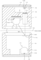
- FIG. 1 is a cross-sectional view of a portion in the vicinity of a center portion in a longitudinal direction of a CIS.
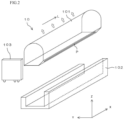
- FIG. 2 is an exploded perspective view.
- An X direction is a main scanning direction
- a Y direction is a sub-scanning direction.
- a Z direction is orthogonal to the X direction and the Y direction.
- a light source unit 10 having a linear shape is an illumination optical system having light amount distribution elongated in the main scanning direction.
- two housings 16 are arranged to face each other across a focal plane (inspection surface) 20.
- the light source unit 10 having a linear shape for illuminating an inspection object on the focal plane 20 is provided.
- a light receiving lens 11 and a light receiving unit 12 are provided, and light from an illuminated inspection object is guided to the light receiving unit 12 by the light receiving lens 11.
- the light receiving lens 11 is an optical element that forms an image of light from an inspection object on the light receiving unit 12.
- one of two of the light source units 10 is arranged on the light receiving unit 12 side with respect to the focal plane 20, and the other is arranged on the opposite side to the light receiving unit 12 side.
- the light receiving unit 12 is mounted on a substrate 13 fixed to one of the housings 16. Light having passed through the light receiving lens 11 is received by a light receiving surface 12A of the light receiving unit 12, and a signal corresponding to an amount of received light is output from the light receiving unit 12.
- a signal corresponding to an amount of received light is output from the light receiving unit 12.
- an inspection object is conveyed in one direction Y along the focal plane 20, light from the inspection object is continuously received by the light receiving unit 12, and an image (color image, fluorescence image, or the like) of the inspection object is obtained based on an output signal from the light receiving unit 12.
- an inspection object conveyed in the sub-scanning direction (Y direction) is read by the light receiving unit 12 extending in the main scanning direction (X direction) on a reading line configured by the light receiving surface 12A of the light receiving unit 12.
- Light B3 emitted from one of the light source units 10 passes through protective glass 14 fixed to the housing 16, is reflected by a reflecting member 17A provided on an inner surface of protective glass 14A fixed to the other one of the housings 16, and is guided to the focal plane 20.
- An ultraviolet light blocking filter (UV cut filter) 15 that prevents ultraviolet light from entering the light receiving unit 12 is provided at an optional position from the focal plane 20 to the light receiving unit 12.
- a color filter 18 that allows visible light in a specific wavelength range to pass through is provided between the light receiving unit 12 and the ultraviolet light blocking filter 15.
- a substrate 5 for fixing a light source 103 (ultraviolet light source, visible light source, or the like) provided in the light source unit 10 is installed.
- the light source unit 10 includes a transparent light guide body 101 extending along a longitudinal direction L, the light source 103 provided in the vicinity of one end surface in the longitudinal direction L, and a cover member 102 for holding each side surface of the light guide body 101.
- Light emitted from the light source 103 is incident on the light guide body 101, appropriately reflected in a light diffusion pattern P while propagating in the light guide body 101, and emitted from a light exit surface in an arrow direction to illuminate an inspection object as linear illumination light.
- a depth of field of such a CIS is small, and in a case where an inspection obj ect is thick, it is difficult to perform an inspection in the entire thickness direction, and, since W.D. is narrow, the CIS comes into contact with the inspection object, and the inspection itself is not performed in many cases.
- a SELFOC (manufactured by Nippon Sheet Glass Corporation) lens array is used as the light receiving lens 11.
- the SELFOC lens array is an upright equal-magnification lens array.
- cylindrical SELFOC lenses are stacked in a trefoil shape to form a multi-eye lens.
- An advantage of the multi-eye lens is that what is called brightness of a lens can be made brighter than a single lens. That is, the F-number in a case where a plurality of single lenses are arranged to form a multi-eye lens is smaller than the F-number of a single lens.
- An advantage of the CIS as described above is disadvantageous from the viewpoint of a depth of field and a depth of focus.
- the larger the numerical aperture the smaller a depth of field becomes.
- N.A. a depth of field decreases as the magnification increases.
- N.A. a depth of field decreases as the magnification increases.
- N.A. a depth of field decreases as the magnification increases.
- a length of a depth of field is clearly shown, and adjustment is performed with a diaphragm in order to secure a depth of field. That is, N.A. is changed to obtain a desired depth of field.
- an upright multi-eye lens typified by the SELFOC lens has a structure in which an image is likely blurred in a case where an inspection object changes in an optical axis direction as compared with a monocular lens because optical axes of lenses are different from each other and intersect each other.
- the above is a major disadvantage of a multi-eye SELFOC lens array in a trefoil stacking system. In view of the above, as a result of examining how a depth of field of a compact optical line sensor can be increased, an obtained example will be described below.
- FIG. 3 is a schematic diagram of a light receiving system in which visual fields 111 of the light receiving lenses 11 do not substantially overlap. That is, in FIG. 3 , the light receiving lenses 11 are arranged in a manner separated from each other in the main scanning direction (X direction) so that the visual fields 111 of the light receiving lenses 11 do not substantially overlap each other.
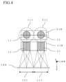
- a plurality of the light receiving lenses 11 arranged along the main scanning direction (X direction) are arranged in a manner separated from each other by a diameter of the light receiving lens 11 or more. This is shown in FIG. 4 .
- a part of the light receiving system of FIG. 3 is illustrated in a side view, but a plan view of the part of the light receiving system is also illustrated for visual clarity.
- a plurality of the light receiving lenses 11 are integrally held by a lens holder 110.
- a light receiving element array 120 formed of a plurality of light receiving elements (not illustrated) arranged linearly along the main scanning direction (X direction) is arranged at a position facing a plurality of the light receiving lenses 11 in the Z direction.
- one light receiving element array 120 is configured as a plurality of light receiving elements are arranged in an array of one row. In this manner, a plurality of light receiving elements form one reading line L. Each light receiving element receives light transmitted through each of the light receiving lenses 11.
- a plurality of the light receiving lenses 11 are preferably arranged in a manner separated from each other within a visual field dimension (within a visual field range) of the light receiving lens 11.
- a plurality of the light receiving lenses 11 are arranged to be separated from each other with substantially the same dimension as a visual field dimension of each of the light receiving lenses 11, but visual field radii of the light receiving lenses 11 may be placed on each other.
- subtraction processing is preferably performed for pixel output from the light receiving element for a light receiving element in a portion where the visual fields 111 of a plurality of the light receiving lenses 11 overlap.
- an image of one of the light receiving lenses 11 is preferably excluded from data output from the light receiving element, or pixel output from the light receiving element is preferably set to a substantially half output value at the time of image synthesis.
- the light receiving element arrays 120 may be arranged to be separated in the sub-scanning direction (Y direction).
- a plurality of light receiving elements are arranged in an array of a plurality of rows (for example, two rows) to constitute a plurality of the light receiving element arrays 120, and form a plurality of rows of the reading lines L.
- a plurality of the light receiving element arrays 120 may be of a multi-line system, or may be of a system in which short light receiving element rows are arranged in a staggered manner.
- FIG. 5 is a schematic diagram illustrating an example of a light receiving system in which a plurality of the light receiving element arrays 120 are arranged.
- at least a part of a plurality of the light receiving lenses 11 are arranged to be separated from each other by a visual field dimension of the light receiving lens 11 or more in the main scanning direction (X direction), and at least two rows (two rows in this example) of the reading lines L are formed by the multi-line system.
- a separation distance of the light receiving element arrays 120 in the sub-scanning direction (Y direction) is preferably larger than a visual field dimension of the light receiving lens 11 as illustrated in FIG. 5 .
- the visual fields 111 may overlap.
- a position where the visual fields 111 overlap may be corrected in advance with a correction chart or the like for correcting pixel output from a light receiving element.
- the visual fields 111 do not need to be placed on each other, and the optical line sensor can be made compact.
- FIG. 6A is a schematic diagram illustrating another example of a light receiving system in which a plurality of the light receiving element arrays 120 are arranged.
- the light receiving element arrays 120 including a short sensor are arranged in a staggered manner so as to be separated from each other by the visual field 111 of the light receiving lens 11 or more in the sub-scanning direction (Y direction).
- Y direction sub-scanning direction
- An optical axis of each of the light receiving lenses 11 may penetrate a substantially center portion in the main scanning direction (X direction) of each of the light receiving element arrays 120 in a one-to-one correspondence.
- a plurality of the light receiving element arrays 120 are arranged in a plurality of rows in the sub-scanning direction (Y direction). That is, the light receiving element arrays 120 in a plurality of rows are arranged in a manner separated from each other in a direction (Y direction) perpendicular to the arrangement direction (X direction) of the light receiving element.
- FIG. 6B is a schematic diagram illustrating still another example of the light receiving system in which a plurality of the light receiving element arrays 120 are arranged.
- the light receiving element arrays 120 including a long sensor are arranged as line sensors having the same length while being separated from each other by the visual field 111 of the light receiving lens 11 or more in the sub-scanning direction (Y direction).
- Y direction sub-scanning direction
- one of the light receiving element arrays 120 may correspond to a plurality of the light receiving lenses 11 arranged in the main scanning direction (X direction), so that a plurality of the light receiving element arrays 120 may be arranged as many as the number of rows of the light receiving lenses 11 in the sub-scanning direction (Y direction).
- each of a plurality of the light receiving element arrays 120 are arranged to be separated from each other by a visual field dimension of the light receiving lens 11 or more in the sub-scanning direction (Y direction) orthogonal to the reading line L.
- the present invention is not limited to such a configuration, and a plurality of the light receiving element arrays 120 may be separated from each other by a diameter of the light receiving lens 11 or more in the sub-scanning direction (Y direction) orthogonal to the reading line L, and may be separated from each other by a visual field dimension of the light receiving lens 11 or less.
- the short light receiving element arrays 120 may be used in staggered arrangement (see FIG.
- the present invention is not limited to this configuration, and a larger number of the light receiving element arrays 120 may be arranged to be separated from each other in the sub-scanning direction (Y direction).
- FIG. 6C illustrates a case where one row of the light receiving lenses 11 are arranged in parallel to the light receiving element array 120 at a substantially center portion in the sub-scanning direction (Y direction) of two rows of the light receiving element arrays 120 arranged in a staggered manner.
- the common light receiving lens 11 are arranged in the sub-scanning direction (Y direction).
- a plurality of the light receiving element arrays 120 arranged in two rows of the reading lines L are shorter than the reading line L, and are separated from each other in the main scanning direction (X direction).
- the light receiving element array 120 arranged in one of the reading lines L and the light receiving element array 120 arranged in the other one of the reading lines L are alternately arranged in a staggered manner along the main scanning direction (X direction). Between two rows of the reading lines L, a plurality of the light receiving lenses 11 are arranged in one row in parallel to a plurality of the light receiving element arrays 120, and an optical axis of each of the light receiving lenses 11 penetrates substantially a center portion in the sub-scanning direction (Y direction) of two rows of the reading lines L. In this case, even if the light receiving lenses 11 are in one row, light transmitted through each of the light receiving lenses 11 can be received by two rows of the light receiving element arrays 120.
- a CIS of a conventional system has large N.A.
- occurrence of image blurring due to a diffraction limit has been ignorable.
- N.A. a focal length of a light receiving lens
- the present embodiment proposes a method in which a lens diameter is increased so that W.D. is increased, and optical resolution is not degraded even in a case where image blur due to a diffraction limit is reduced.
- FIG. 7 shows a relationship between N.A. and a diffraction limit for each wavelength.
- a pitch of the light receiving lens 11 itself is shortened, a focal length increases, and influence of aberration also decreases.
- the above shows that it is necessary to further increase a lens diameter in order to lengthen a focal length of the light receiving lens 11.
- influence of diffraction can be made equal to that of the light receiving lens 11 having short focus.
- geometrical optical aberration increases.
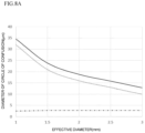
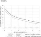
- FIG. 8A illustrates a relationship between an effective diameter of the SELFOC lens A and a diameter of a circle of confusion
- FIG. 8A illustrates a relationship between an effective diameter of the SELFOC lens A and a diameter of a circle of confusion
- FIGS. 8A to 8C illustrate a relationship between an effective diameter of the SELFOC lens B and a diameter of a circle of confusion
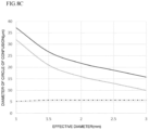
- FIG. 8C illustrates a relationship between an effective diameter of the SELFOC lens C and a diameter of a circle of confusion.
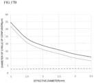
- a solid line indicates a total circle of confusion
- a broken line indicates a circle of confusion due to diffraction
- an alternate long and short dash line indicates a geometric optical circle of confusion.
- FIGS. 7 and 8A a relationship between a least circle of confusion and a diffraction limit, that is, optical resolution at a certain lens diameter and a focal length can be seen. Therefore, in the case of the light receiving lens 11 illustrated in FIG. 8A , as an effective diameter ⁇ increases, a diameter of a circle of confusion decreases, and the effective diameter ⁇ is shown to be preferably 1.0 mm ⁇ ⁇ ⁇ 3.0 mm.
- the light receiving lens 11 illustrated in FIG. 8A is a SELFOC lens having smaller aberration and a larger effective diameter than the light receiving lens 11 illustrated in FIG. 8B , and it can be seen that the light receiving lens 11 in FIG. 8A should be selected. Furthermore, in the light receiving lens 11 in FIG. 8A having the same focal length, N.A.
- a scanning speed of the light receiving lens 11 in FIG. 8A can be considered to be improved by nine times as compared with the light receiving lens 11 in FIG. 8B .
- the SELFOC lens C similarly to the SELFOC lens A, the SELFOC lens C has less aberration and can have a large effective diameter.
- a parameter of the SELFOC lenses A to C illustrated in FIGS. 8A to 8C is illustrated in Table 1 below.
- the most important parameter in Table 1 is a refractive index distribution constant.
- the light receiving lens 11 having low aberration when an effective diameter is increased and a focal length is extended is the SELFOC lens A having the smallest refractive index distribution constant, and the light receiving lens 11 having next lower aberration is the SELFOC lens C.
- the light receiving lens 11 having a large effective diameter, being bright, and having less aberration is preferable in order to achieve high resolution and high speed inspection.
- [Table 1] Focal length (mm) On-axis refractive index Refractive index distribution constant (1/mm) SELFOC lens A 50 1. 615 0. 077 SELFOC lens B 0. 154 SELFOC lens C 0. 103
- FIG. 9A illustrates a relationship between an effective diameter of a rod lens A and a diameter of a circle of confusion
- FIG. 9B illustrates a relationship between an effective diameter of a rod lens B and a diameter of a circle of confusion
- FIG. 9C illustrates a relationship between an effective diameter of a rod lens C and a diameter of a circle of confusion
- FIG. 9D illustrates a relationship between an effective diameter of a rod lens D and a diameter of a circle of confusion.
- FIGS. 9A illustrates a relationship between an effective diameter of a rod lens A and a diameter of a circle of confusion
- FIG. 9B illustrates a relationship between an effective diameter of a rod lens B and a diameter of a circle of confusion
- FIG. 9C illustrates a relationship between an effective diameter of a rod lens C and a diameter of a circle of confusion
- FIG. 9D illustrates a relationship between an effective diameter of a rod lens D and a diameter of a circle of confusion.
- a solid line indicates a total circle of confusion
- a broken line indicates a circle of confusion due to diffraction
- an alternate long and short dash line indicates a geometric optical circle of confusion.
- a parameter of the rod lenses A to D illustrated in FIGS. 9A to 9D is illustrated in Table 2 below. It can be seen that the plastic rod lens also has the same tendency as the SELFOC lens. Considering a refractive index of a plastic rod lens and a refractive index of a glass lens, an on-axis refractive index is preferably about 1.45 to 1.65. [Table 2] Focal length (mm) On-axis refractive index Refractive index distribution constant (1/mm) Rod lens A 5 0 1. 491 0. 28 Rod lens B 0. 14 Rod lens C 0. 105 Rod: lens D 0. 07
- a refractive index distribution constant is a dominant factor of aberration.
- aberration is lowered as a refractive index gradually changes. This is similar to a case where even in a normal spherical lens, a sudden angle change is a cause of occurrence of aberration.
- a sudden angle change means an increase in a high-order nonlinear effect when Snell' Law is subjected to polynomial expansion. That is, since deviation from paraxial optics becomes large, aberration becomes large.
- a refractive index distribution constant is preferably 0.12 or less in order to achieve pixel resolution with a resolution of 400 dpi or more when a focal length or W.D. is approximately 50 mm or more and the effective diameter ⁇ is approximately ⁇ ⁇ 1.0 mm.
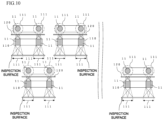
- FIG. 10 is a schematic diagram in a case where the receiver lens 11 is an upright reducing multi-eye lens instead of an upright equal magnification multi-eye lens.
- FIG. 10 illustrates a schematic diagram in a case where light receiving lenses 11 are separated by a visual field dimension of the light receiving lenses 11 or more, and the light receiving element arrays 120 are arranged to be separated by a visual field dimension of the light receiving lenses 11 or more in a direction orthogonal to the reading line L.
- a part of a light receiving system is illustrated in a plan view, but a side view of the part of the light receiving system is also illustrated for visual clarity.
- a depth of field can be increased significantly as compared with the upright equal magnification lens described above.
- a depth of field is increased by two times.
- a depth of field is three times as large.
- pixel dimension of a light receiving element is also made smaller than pixel dimension in an equal magnification system according to reduction magnification and according to desired resolution.
- the same pixel dimension as that of an equal magnification system may be used depending on resolution.
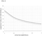
- FIG. 11 illustrates a relationship between an effective diameter of a reduction lens and a diameter of a circle of confusion.
- the light receiving lens 11 in the invention of the present application is not limited to a refractive index distribution type lens such as a SELFOC lens or a plastic rod lens, and in other lenses, for example, an achromatic lens, an apochromatic lens, and the like, in consideration of cost, it is also possible to use a lens in which aberration due to a non-linear effect in the refractive index distribution type lens is equalized, that is, spherical aberration, coma aberration, and astigmatism are equalized, or a telecentric refractive optical system in the same arrangement and dimension (aperture) instead of a refractive index distribution type lens such as a SELFOC lens or a plastic rod lens in which aberrations due to a non-linear effect in the refractive index distribution type lens and a diffraction limit are equivalent.
- a refractive index distribution type lens such as a SELFOC lens or a plastic rod lens in which aberrations due to a non-linear
- the above-described optical system is of a case where an upright lens is used at the center, but may be an inverted optical system in a case where the visual fields 111 do not overlap. That is, a plurality of the light receiving lenses 11 may be configured to form an inverted image. As long as an lens array is of a two-row system, an inverted optical system can be employed. In a case of an inverted optical system, since an image is inverted and symmetric about an optical axis, an inverted image is preferably converted into an erected image by image processing at the time of image synthesis. That is, an inverted image of a plurality of the light receiving lenses 11 is preferably inverted and converted into an erected image, and then image synthesis processing is preferably performed.
- necessity or unnecessity of an overlapping portion is preferably determined and corrected by a correction algorithm, and conversion into an erect image is preferably performed based on a determined relationship between the pixels.
- a correction algorithm in inspection in a case where an image is not constructed, it is only necessary to detect a flaw or a defect, and thus, it is not necessary to perform image synthesis and image processing, and detected portions on an inspection surface may be superimposed. In the case of superimposition, correction of a position by a correction chart is performed in advance.
- inverted refractive optical system in signal processing for each light receiving element, for example, data obtained from one of two rows of light receiving element arrays arranged in a staggered manner so as to be separated in the sub-scanning direction may be acquired longer, data obtained from the other light receiving element array may be acquired shorter, inversion operation to an erected image may be performed for an acquired image, and then image synthesis may be performed.
- a correction coefficient may be multiplied by or subtracted from portions that overlap at the time of image synthesis.
- a plurality of light receiving element arrays may be light receiving element arrays shorter than a plurality of reading lines arranged in two rows of reading lines. Further, a light receiving element arrays arranged in one of reading lines and a light receiving element arrays arranged in the other one of the reading lines may be alternately arranged in a staggered manner along the main scanning direction. Such a configuration is similar to the case of the upright refractive optical system described in FIG. 6A , and thus detailed description of the configuration will be omitted.
- a plurality of light receiving elements are arranged in arrays of two or more rows to constitute a plurality of the light receiving element arrays 120. Further, each of a plurality of the light receiving element arrays 120 is arranged to be separated from each other by a visual field dimension or more of the light receiving lens 11 in a direction orthogonal to the reading line L.
- a plurality of the light receiving lenses 11 are arranged as many as a plurality of the light receiving element arrays 120, and an optical axis of each of the light receiving lenses 11 passes through a substantially center portion of each of the light receiving element arrays 120.
- a high-luminance white LED array is used as the light source 103. That is, a plurality of the light sources 103 may be configured to include a white LED.
- an emitted beam is enlarged in the main scanning direction and collimated in the sub-scanning direction to reduce light amount unevenness at the time of irradiation.
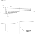
- FIG. 12A illustrates one example of an arrangement method in a case where an RGB-LED or an RGB-LD (laser diode; semiconductor laser) is used as the light source 103.
- a plurality of the light sources 103 may be configured to include a red LED (R), a green LED (G), and a blue LED (B), or may be configured to include a laser diode.
- a plurality of the light sources 103 are mounted on a light source substrate 134, and a heat sink 135 is attached to the light source substrate 134.
- a beam emitted from each of the light sources 103 is collimated by a condenser lens 104 having an ellipsoidal shape in which lens power is different between the main scanning direction and the sub-scanning direction, and is applied to an inspection object.
- the condenser lens 104 having an ellipsoidal shape is described, but any lens may be used as long as lens power is appropriately different between the main scanning direction and the sub-scanning direction.
- power of a lens is a reciprocal of a focal length and is a measure representing refractive power of a lens.
- the LD may be a normal collimator lens as long as an end surface emission type LD in which a spread angle of an emission beam of the LD itself is different between the horizontal direction and the vertical direction is used.
- FIG. 12B is a side view illustrating a specific example of an arrangement method in a case where an LD is used as the light source 103. In this case, an LD having a larger spread angle is arranged in parallel to the main scanning direction. Beams emitted from a red LD 131, a green LD 132, and a blue LD 133 constituting the light source 103 are collimated by the condenser lens 104 associated with each of them, and then, are focused on an inspection surface by a cylindrical lens 105.
- each color of RGB is emitted to substantially the same position in the sub-scanning direction, and color unevenness with respect to the sub-scanning direction can be reduced.
- light emitted by the light source 103 such as an LED or an LD and diffused and reflected by an inspection surface forms an image on a light receiving element array by a light receiving lens system.
- a light receiving element in an equal magnification optical system, one having an element size of 62 ⁇ m corresponding to 400 dpi to an element size of 42 ⁇ m corresponding to 600 dpi is used. In a case where an element size of 600 dpi or more is used, power of illumination light is preferably increased accordingly.
- a plurality of the light sources 103 may include the light sources 131 to 133 having a plurality of different wavelengths, and a plurality of the light sources 103 in one unit may be configured to be arranged in the main scanning direction (X direction) with the light sources 131 to 133 as one unit.
- an amount of received light decreases in inverse proportion to substantially the square of an area of a light receiving element.
- An illumination light amount is determined in consideration of the above. When an element size decreases, an amount of received light decreases in inverse proportion to an element area in the same accumulation time. This is a physical property of a semiconductor light receiving element, and in order to maintain S/N, an amount of illumination light is preferably increased to increase power density, and the number of generated electrons generated per unit time is preferably made the same.
- light received by a light receiving element depends not only on illuminance of an inspection surface but also on a range viewed by a light receiving element when light is received. Needless to say, if a solid angle of light reception is different and the angle decreases, an amount of received light also decreases, and if an inspection surface is a perfect diffusion surface, an amount of received light is in accordance with what is called the cos ⁇ law.
- Light that is diffused and reflected from an inspection surface is captured by a light receiving lens and condensed on a light receiving element, and an output signal of the light is output from the light receiving element. Further, an output signal from a light receiving element array is branched from serial to parallel so that processing speed is improved and is transmitted to an image processing device.
- FIGS. 13A and 13B illustrate a positional relationship between the light source 103 and a light receiving system.
- FIG. 13A is a schematic diagram illustrating an example of a positional relationship between the light source 103 and a light receiving system, and illustrates a case where two rows of the light receiving element arrays 120 are arranged in a staggered manner in a short sensor or as line sensors having the same length in a long sensor (length corresponding to the entire length in the main scanning direction) in a manner separated by a distance larger than the visual field 111 of the light receiving lens 11.
- FIG. 13B is a schematic diagram illustrating another example of a positional relationship between the light source 103 and a light receiving system, and illustrates that the light receiving lens 11 is arranged in the main scanning direction such that the visual fields 111 of the light receiving lens 11 do not substantially overlap.
- FIG. 14A is a schematic diagram illustrating a positional relationship between the light source 103 and the light receiving lens 11, and illustrates a case of one row of the light receiving element arrays 120.
- a position of the light source 103 is determined such that a minimum value of unevenness on an inspection surface of illumination light of the light source 103 is located in a substantially center portion of the light receiving element array 120.
- the light source 103 is determined at a position on a virtual plane perpendicular to the main scanning direction including a substantially center portion between the light receiving lenses 11 adjacent to each other in the main scanning direction (X direction) in consideration of absolute irradiance on an inspection surface.
- the light sources 103 are arranged in parallel to the reading line L.
- an optical axis of each of the light sources 103 is arranged at an optional position on a virtual plane which forms an intersection with an optical axis of each of the light receiving lenses 11 and intersects an optical axis of each of the light receiving lenses 11.
- the light source 103 is arranged at a substantially center portion between the light receiving lenses 11 adjacent to each other.
- light is emitted from the light source 103 at an angle of about 45 degrees with respect to an inspection surface. For this reason, a distance between the light source 103 and an inspection surface is set to 70 mm in consideration of W.D. of the light receiving lens 11.
- an LD is used, but an LED of each wavelength may be used.
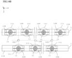
- FIG. 14B is a schematic diagram illustrating a positional relationship between the light source 103 and the light receiving lens 11, and illustrates a case of two rows of the light receiving element arrays 120.
- a lens parameter is the same as that in FIG. 14A .
- FIG. 14B arrangement of the light sources 103 with respect to the light receiving lenses 11 and the light receiving element arrays 120 arranged in two rows is illustrated.
- the light source 103 is arranged in a substantially center portion of two of the reading lines L. A portion different from the case of FIG.
- an arrangement pitch of the light receiving lenses 11 may be wider than a lens diameter
- an arrangement pitch of the light sources 103 is also matched with an inter-lens distance
- the light sources 103 are arranged at positions which are substantially center portions between the light receiving lenses 11 adjacent to each other and are substantially center portions of two rows of the reading lines L at the same time. This makes it possible to further prevent missing of a pixel on an inspection surface, and at the same time, it is possible to further reduce shading of the light receiving lens 11 and light amount unevenness of the light source 103.
- a positional relationship between the light source 103 and an inspection surface is the same as that in the case of FIG. 14A .
- a lens pitch between the light receiving lenses 11 in each row is set to 7 mm. In this case, a substantial lens pitch is 3.5 mm.
- FIG. 14C is a diagram illustrating a relationship between light amount distribution of the light source 103 (on an inspection surface), light amount distribution on a light receiving element surface, and shading of the light receiving lens 11 in the main scanning direction.
- light amount distribution on the light receiving element array 120 becomes flat as schematically illustrated in FIG. 14C , and a dynamic range of the light receiving element can be effectively used.
- an inspection object is irradiated with illumination light having negative intensity distribution by an illumination system in advance.
- a method of arranging the light source 103 between adjacent ones of the light receiving lenses 11 is not a shading prevention method that completely supports various types of the light receiving lenses 11. That is, if there is shading unique to each of the light receiving lenses 11 and the light receiving lenses 11 are different, it is necessary to use an illumination optical system corresponding the light receiving lenses 11.
- the condenser lens 104 having large power is arranged in the main scanning direction. A light flux transmitted through the condenser lens 104 is then guided to an inspection object by a converging lens such as the cylindrical lens 105, and light intensity corresponding to shading of the light receiving lens 11 is formed on the inspection object.
- the condenser lens 104 may have power in the sub-scanning direction. In short, it is only necessary to completely prevent shading of the light receiving lens 11 and, at the same time, to achieve effective light intensity distribution in consideration of a focal length of the light receiving lens 11 with respect to an inspection object. That is, an optical element in which lens power in the main scanning direction is larger than lens power in the sub-scanning direction is preferable.
- the condenser lens 104 for example, a cylindrical lens, a lenticular lens, a Fresnel lens, or a combination of a prism sheet and a spherical lens is preferable.
- the light source 103 may be arranged at an intermediate position of each of the light receiving lenses 11, or may be arranged on an optical axis of the light receiving lens 11.
- the light source 103 may be arranged at a position on an outer periphery of the light receiving lens 11.
- a lens having a power distribution in the main scanning direction is more preferable.
- the condenser lens 104 that condenses a light flux from a plurality of the light sources 103 is provided as one lens body, and power in the main scanning direction of the lens body is larger than power in the sub-scanning direction.
- the condenser lens 104 may be configured to include a first condenser lens and a second condenser lens instead of a single lens body.
- power in the main scanning direction may be larger than power in the sub-scanning direction
- power in the sub-scanning direction may be larger than power in the main scanning direction.
- power in the main scanning direction may be adjustable with the first condenser lens and the second condenser lens.
- the first condenser lens and the second condenser lens can be constituted by a cylindrical lens, a lenticular lens, a Fresnel lens, a prism array, or the like.
- the first condenser lens may be a lenticular lens or a prism array.
- the second condenser lens may be a Fresnel lens or a cylindrical lens.
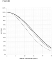
- FIG. 14D A graph of a light receiving system MTF for each lens diameter in the present embodiment is illustrated in FIG. 14D .
- the lens is preferably made from glass or resin.
- an on-axis refractive index N 0 is preferably 1.45 ⁇ N 0 ⁇ 1.65
- the refractive index distribution constant ⁇ A is preferably 0.05 ⁇ ⁇ A ⁇ 0.12
- the focal length f is preferably 50 mm ⁇ f ⁇ 150 mm.
- the light receiving lens 11 may be an achromatic or apochromatic lens in which a plurality of lenses is combined.
- a lens system in which only a convex lens is combined as a plurality of lenses may be used, or a lens system in which a convex lens and a concave lens are combined as a plurality of lenses may be used.
- the focal length f of a plurality of lenses is preferably 50 mm ⁇ f ⁇ 250 mm
- an aperture ⁇ of a plurality of lenses is preferably 2 mm ⁇ ⁇ ⁇ 10 mm.
- a configuration of the optical system is similar to that in FIGS. 14A and 14B , and magnification of the light receiving lens 11 is changed. That is, a relationship in lateral magnification between an object point and an image point of the light receiving lens 11 is changed to 9:1, 4:1, or the like. In this manner, a depth of field is increased to three times that in the equal magnification system in a case where the lateral magnification is 9:1, and is increased to two times that in the equal magnification system in a case where the lateral magnification is 4:1.
- size of a light receiving element is set to 1/9 of size of a light receiving element in the equal magnification system. Further, in a case where a depth of field is set to two times as large, size of a light receiving element is set to 1/4 of size of a light receiving element in the equal magnification system. In the present embodiment, a light receiving element having size of 1/4 is used, and a depth of field set to two times as large.
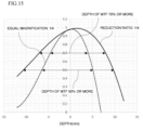
- An MTF characteristic at the time of defocusing of a reduction optical system in the present embodiment is illustrated in a graph (solid line) of FIG. 15 .
- an MTF characteristic at the time of defocusing in the equal magnification system is illustrated in a graph (broken line) of FIG. 15 .
- Comparison between the reduction system and the equal magnification system in the diagram shows that a depth of field of the reduction optical system is about twice larger than that of the equal magnification system. Further, if a reduction ratio is S, N.A. of the light receiving lens 11 is increased by 1/S which is a reciprocal of S.
- FIG. 14A a method of preventing occurrence of crosstalk due to superimposition of the visual fields 111 will be described.
- FIG. 16A illustrates a configuration of a visual field limiting holder in which the light receiving element array 120 side of the lens holder 110 is extended in a cylindrical shape. An effect of the configuration will be described below.
- FIG. 16B A detailed diagram is illustrated in FIG. 16B .
- a plurality of the light receiving lenses 11 are inserted into the lens holder 110, and an aperture 112 including a through hole is formed on the light receiving element array 120 side of each of the light receiving lenses 11.
- An outer diameter of a plurality of the light receiving lenses 11 is a clearance fit dimension with respect to an inner diameter of the lens holder 110, and clearance fitting is performed by inserting each of the light receiving lenses 11 into the lens holder 110.
- Each of the apertures 112 has an inner diameter smaller than an outer diameter of each of the light receiving lenses 11, and extends along an optical axis of each of the light receiving lenses 11.
- the side of a plurality of the light receiving elements (the light receiving element array 120 side) of the lens holder 110 is extended in a cylindrical shape by each of the apertures 112, so that the visual field 111 of each light receiving lens 11 is limited.
- the cylindrical shape means a configuration in which the aperture 112 is extended by a through hole formed in a cylindrical shape, but is not limited to this configuration, and the aperture 112 may be extended in a flat plate shape by a protruding flat plate. Between adjacent ones of the light receiving lenses 11, lengths on the side of a plurality of light receiving elements (the light receiving element array 120 side) of the lens holder 110, that is, lengths of the apertures 112 may be different.
- the light flux is not limited in the visual field by the aperture 112 and can be received by the light receiving element array 120, but a light flux outside the visual field 111 (outside with respect to an optical axis of the light receiving lens 11) does not reach the light receiving element array 120. That is, a light flux within the visual field 111 of the light receiving lens 11 reaches a light receiving element facing the light receiving lens 11, but a light flux outside the visual field 111 does not reach any of a light receiving element facing the light receiving lens 11 and an adjacent light receiving element.
- the aperture 112 does not need to have a cylindrical shape.
- a partition may be provided at an intermediate position between the light receiving lenses 11 to prevent light received by the light receiving lenses 11 from being received by another one of the light receiving lenses 11.
- a plurality of the light receiving lenses 11 is not limited to those in a configuration of being arranged in a row, and may be arranged in a trefoil stacking shape by inserting and fixing a single one of the light receiving lenses 11 into a cylindrical holder in advance and then stacking the cylindrical holders in a trefoil shape. Further, a plurality of the light receiving lenses 11 may be positioned by an L-shaped positioning jig, bonded and fixed, and then stored in a rectangular lens holder.
- the aperture 112 is provided on the light receiving element array 120 side, but may be provided on an inspection surface side with a length that does not impair W.D. Then, a combination of an aperture on the inspection surface side and an aperture on the light receiving element side enables more effective visual field limitation.
- the effective diameter ⁇ is in the same aspect as that in the case of FIG. 14A .
- a solid line indicates a total circle of confusion
- a broken line indicates a circle of confusion due to diffraction
- an alternate long and short dash line indicates a geometric optical circle of confusion. Note that, in any of FIGS.
- a diameter of a circle of confusion including diffraction is much smaller than about 43 ⁇ m of a case where resolution is aimed at 600 dpi.
Landscapes
- Physics & Mathematics (AREA)
- Engineering & Computer Science (AREA)
- Signal Processing (AREA)
- General Physics & Mathematics (AREA)
- Multimedia (AREA)
- General Health & Medical Sciences (AREA)
- Health & Medical Sciences (AREA)
- Pathology (AREA)
- Biochemistry (AREA)
- Immunology (AREA)
- Analytical Chemistry (AREA)
- Chemical & Material Sciences (AREA)
- Life Sciences & Earth Sciences (AREA)
- Optics & Photonics (AREA)
- Toxicology (AREA)
- Computer Vision & Pattern Recognition (AREA)
- Textile Engineering (AREA)
- Facsimile Heads (AREA)
- Facsimile Scanning Arrangements (AREA)
- Image Input (AREA)
Applications Claiming Priority (2)
| Application Number | Priority Date | Filing Date | Title |
|---|---|---|---|
| JP2020207542A JP7470028B2 (ja) | 2020-12-15 | 2020-12-15 | 光学ラインセンサ |
| PCT/JP2021/036486 WO2022130736A1 (fr) | 2020-12-15 | 2021-10-01 | Capteur de ligne optique |
Publications (2)
| Publication Number | Publication Date |
|---|---|
| EP4266661A1 true EP4266661A1 (fr) | 2023-10-25 |
| EP4266661A4 EP4266661A4 (fr) | 2024-05-29 |
Family
ID=82059702
Family Applications (1)
| Application Number | Title | Priority Date | Filing Date |
|---|---|---|---|
| EP21906100.9A Pending EP4266661A4 (fr) | 2020-12-15 | 2021-10-01 | Capteur de ligne optique |
Country Status (6)
| Country | Link |
|---|---|
| US (1) | US12541096B2 (fr) |
| EP (1) | EP4266661A4 (fr) |
| JP (1) | JP7470028B2 (fr) |
| KR (1) | KR20230106677A (fr) |
| CN (1) | CN116685879A (fr) |
| WO (1) | WO2022130736A1 (fr) |
Families Citing this family (3)
| Publication number | Priority date | Publication date | Assignee | Title |
|---|---|---|---|---|
| JP7706659B2 (ja) * | 2022-06-08 | 2025-07-11 | 株式会社ヴィーネックス | 光学ラインセンサ |
| CN119999178A (zh) * | 2022-11-18 | 2025-05-13 | 株式会社维纳科斯 | 受光透镜阵列及光学线传感器、以及受光透镜阵列的制造方法 |
| JP7733782B1 (ja) | 2024-08-06 | 2025-09-03 | 株式会社ヴィーネックス | 光学ラインセンサ及び表面検査装置 |
Family Cites Families (17)
| Publication number | Priority date | Publication date | Assignee | Title |
|---|---|---|---|---|
| JPH0514600A (ja) | 1991-06-28 | 1993-01-22 | Kyocera Corp | 原稿読み取り装置 |
| JP2815130B2 (ja) | 1992-11-04 | 1998-10-27 | キヤノン株式会社 | レンズアレイ及びそれを用いた密着型イメージセンサー |
| US5566254A (en) | 1992-11-06 | 1996-10-15 | Canon Kabushiki Kaisha | Apparatus for processing multiple images in alternating fashion |
| US6707613B2 (en) * | 2000-04-05 | 2004-03-16 | Rohm Co., Ltd. | Lens array unit and method of forming image |
| JP4210174B2 (ja) | 2003-07-18 | 2009-01-14 | ソニー株式会社 | 変倍ファインダおよび撮像装置 |
| JP4913089B2 (ja) | 2008-03-31 | 2012-04-11 | 三菱電機株式会社 | 画像読取装置 |
| JP4809859B2 (ja) | 2008-03-31 | 2011-11-09 | 三菱電機株式会社 | 画像読取装置 |
| JP2010224164A (ja) * | 2009-03-23 | 2010-10-07 | Nippon Sheet Glass Co Ltd | 正立等倍レンズアレイプレート、光走査ユニットおよび画像読取装置 |
| JP5417554B1 (ja) | 2012-03-30 | 2014-02-19 | 三菱レイヨン株式会社 | ロッドレンズアレイおよびそれを用いたイメージセンサヘッド |
| JP6230222B2 (ja) | 2012-10-12 | 2017-11-15 | キヤノン株式会社 | レンズアレイ光学系及びレンズアレイの製造方法 |
| JP2015025972A (ja) | 2013-07-26 | 2015-02-05 | 京セラ株式会社 | レンズアレイ、画像読取装置、および画像形成装置 |
| DE202015004739U1 (de) | 2015-07-02 | 2016-10-05 | Schwan-Stabilo Cosmetics Gmbh & Co. Kg | Schoner für einen Stift |
| JP6733406B2 (ja) | 2016-07-29 | 2020-07-29 | コニカミノルタ株式会社 | 画像読取装置 |
| JP6708045B2 (ja) | 2016-08-01 | 2020-06-10 | コニカミノルタ株式会社 | 画像読取モジュール、画像読取装置および画像形成装置 |
| KR20180019334A (ko) | 2016-08-16 | 2018-02-26 | 주식회사 엔케이 | 액화가스 저장탱크 |
| JP6870395B2 (ja) | 2017-03-13 | 2021-05-12 | コニカミノルタ株式会社 | 画像読取装置 |
| JP7456092B2 (ja) | 2019-03-26 | 2024-03-27 | 富士フイルムビジネスイノベーション株式会社 | 光学装置、画像読取装置、および画像形成装置 |
-
2020
- 2020-12-15 JP JP2020207542A patent/JP7470028B2/ja active Active
-
2021
- 2021-10-01 WO PCT/JP2021/036486 patent/WO2022130736A1/fr not_active Ceased
- 2021-10-01 KR KR1020237019890A patent/KR20230106677A/ko active Pending
- 2021-10-01 US US18/265,221 patent/US12541096B2/en active Active
- 2021-10-01 EP EP21906100.9A patent/EP4266661A4/fr active Pending
- 2021-10-01 CN CN202180079235.2A patent/CN116685879A/zh active Pending
Also Published As
| Publication number | Publication date |
|---|---|
| KR20230106677A (ko) | 2023-07-13 |
| JP2022094583A (ja) | 2022-06-27 |
| CN116685879A (zh) | 2023-09-01 |
| WO2022130736A1 (fr) | 2022-06-23 |
| EP4266661A4 (fr) | 2024-05-29 |
| US20240027750A1 (en) | 2024-01-25 |
| US12541096B2 (en) | 2026-02-03 |
| JP7470028B2 (ja) | 2024-04-17 |
Similar Documents
| Publication | Publication Date | Title |
|---|---|---|
| US12541096B2 (en) | Optical line sensor | |
| JP4453752B2 (ja) | 画像読取装置 | |
| US7982924B2 (en) | Image reading device | |
| US6987259B2 (en) | Imaging system with an integrated source and detector array | |
| US20110273751A1 (en) | Single led dual light guide | |
| US5978146A (en) | Rod lens array and life-size imaging optical apparatus using the same | |
| EP0814596A2 (fr) | Système de balayage | |
| EP0786814A1 (fr) | Matrice d'éléments photodétecteurs avec compensation des aberrations optiques et des non-uniformités de l'illumination | |
| EP4538684A1 (fr) | Capteur à ligne optique | |
| US20100214630A1 (en) | Document illuminating system and image reader including the same | |
| JP4935886B2 (ja) | 画像読取装置 | |
| JP4965594B2 (ja) | 画像読取装置 | |
| US8274716B2 (en) | Image reading apparatus and method of controlling the same | |
| JP7216240B1 (ja) | 光学装置及びイメージセンサ | |
| WO2023238536A1 (fr) | Capteur de ligne optique | |
| US7576349B2 (en) | Radiation image readout apparatus | |
| JP3940487B2 (ja) | 密着型イメージセンサ | |
| JP2026049301A (ja) | 光学ラインセンサ | |
| US8104256B2 (en) | Imaging optical unit, inspection method for the same, and image reading apparatus | |
| US6930807B1 (en) | Color image reading apparatus | |
| US20070188875A1 (en) | Refractive lens array for scanner application that reduces lateral tolerance sensitivity | |
| JP2025079290A (ja) | カメラ | |
| JP2017173738A (ja) | 画像読取光学系及び画像読取装置 | |
| JP2008078877A (ja) | 画像読取用の結像光学系の調整方法 | |
| JPH05328032A (ja) | 画像読取装置 |
Legal Events
| Date | Code | Title | Description |
|---|---|---|---|
| STAA | Information on the status of an ep patent application or granted ep patent |
Free format text: STATUS: THE INTERNATIONAL PUBLICATION HAS BEEN MADE |
|
| PUAI | Public reference made under article 153(3) epc to a published international application that has entered the european phase |
Free format text: ORIGINAL CODE: 0009012 |
|
| STAA | Information on the status of an ep patent application or granted ep patent |
Free format text: STATUS: REQUEST FOR EXAMINATION WAS MADE |
|
| 17P | Request for examination filed |
Effective date: 20230602 |
|
| AK | Designated contracting states |
Kind code of ref document: A1 Designated state(s): AL AT BE BG CH CY CZ DE DK EE ES FI FR GB GR HR HU IE IS IT LI LT LU LV MC MK MT NL NO PL PT RO RS SE SI SK SM TR |
|
| DAV | Request for validation of the european patent (deleted) | ||
| DAX | Request for extension of the european patent (deleted) | ||
| A4 | Supplementary search report drawn up and despatched |
Effective date: 20240426 |
|
| RIC1 | Information provided on ipc code assigned before grant |
Ipc: H04N 1/031 20060101ALI20240422BHEP Ipc: H04N 1/024 20060101ALI20240422BHEP Ipc: H04N 1/028 20060101ALI20240422BHEP Ipc: G02B 3/00 20060101ALI20240422BHEP Ipc: H04N 1/195 20060101AFI20240422BHEP |