EP4266840A1 - Leiterplatte - Google Patents
Leiterplatte Download PDFInfo
- Publication number
- EP4266840A1 EP4266840A1 EP21906167.8A EP21906167A EP4266840A1 EP 4266840 A1 EP4266840 A1 EP 4266840A1 EP 21906167 A EP21906167 A EP 21906167A EP 4266840 A1 EP4266840 A1 EP 4266840A1
- Authority
- EP
- European Patent Office
- Prior art keywords
- substrate
- transparent
- opaque
- transparent protective
- protective layer
- Prior art date
- Legal status (The legal status is an assumption and is not a legal conclusion. Google has not performed a legal analysis and makes no representation as to the accuracy of the status listed.)
- Pending
Links
Images



Classifications
-
- H—ELECTRICITY
- H05—ELECTRIC TECHNIQUES NOT OTHERWISE PROVIDED FOR
- H05K—PRINTED CIRCUITS; CASINGS OR CONSTRUCTIONAL DETAILS OF ELECTRIC APPARATUS; MANUFACTURE OF ASSEMBLAGES OF ELECTRICAL COMPONENTS
- H05K1/00—Printed circuits
- H05K1/02—Details
- H05K1/0274—Optical details, e.g. printed circuits comprising integral optical means
-
- G—PHYSICS
- G06—COMPUTING OR CALCULATING; COUNTING
- G06F—ELECTRIC DIGITAL DATA PROCESSING
- G06F3/00—Input arrangements for transferring data to be processed into a form capable of being handled by the computer; Output arrangements for transferring data from processing unit to output unit, e.g. interface arrangements
- G06F3/01—Input arrangements or combined input and output arrangements for interaction between user and computer
- G06F3/03—Arrangements for converting the position or the displacement of a member into a coded form
- G06F3/041—Digitisers, e.g. for touch screens or touch pads, characterised by the transducing means
- G06F3/044—Digitisers, e.g. for touch screens or touch pads, characterised by the transducing means by capacitive means
- G06F3/0446—Digitisers, e.g. for touch screens or touch pads, characterised by the transducing means by capacitive means using a grid-like structure of electrodes in at least two directions, e.g. using row and column electrodes
-
- G—PHYSICS
- G06—COMPUTING OR CALCULATING; COUNTING
- G06F—ELECTRIC DIGITAL DATA PROCESSING
- G06F3/00—Input arrangements for transferring data to be processed into a form capable of being handled by the computer; Output arrangements for transferring data from processing unit to output unit, e.g. interface arrangements
- G06F3/01—Input arrangements or combined input and output arrangements for interaction between user and computer
- G06F3/03—Arrangements for converting the position or the displacement of a member into a coded form
- G06F3/041—Digitisers, e.g. for touch screens or touch pads, characterised by the transducing means
- G06F3/044—Digitisers, e.g. for touch screens or touch pads, characterised by the transducing means by capacitive means
- G06F3/0445—Digitisers, e.g. for touch screens or touch pads, characterised by the transducing means by capacitive means using two or more layers of sensing electrodes, e.g. using two layers of electrodes separated by a dielectric layer
-
- H—ELECTRICITY
- H05—ELECTRIC TECHNIQUES NOT OTHERWISE PROVIDED FOR
- H05K—PRINTED CIRCUITS; CASINGS OR CONSTRUCTIONAL DETAILS OF ELECTRIC APPARATUS; MANUFACTURE OF ASSEMBLAGES OF ELECTRICAL COMPONENTS
- H05K3/00—Apparatus or processes for manufacturing printed circuits
- H05K3/02—Apparatus or processes for manufacturing printed circuits in which the conductive material is applied to the surface of the insulating support and is thereafter removed from such areas of the surface which are not intended for current conducting or shielding
- H05K3/06—Apparatus or processes for manufacturing printed circuits in which the conductive material is applied to the surface of the insulating support and is thereafter removed from such areas of the surface which are not intended for current conducting or shielding the conductive material being removed chemically or electrolytically, e.g. by photo-etch process
-
- H—ELECTRICITY
- H05—ELECTRIC TECHNIQUES NOT OTHERWISE PROVIDED FOR
- H05K—PRINTED CIRCUITS; CASINGS OR CONSTRUCTIONAL DETAILS OF ELECTRIC APPARATUS; MANUFACTURE OF ASSEMBLAGES OF ELECTRICAL COMPONENTS
- H05K3/00—Apparatus or processes for manufacturing printed circuits
- H05K3/22—Secondary treatment of printed circuits
- H05K3/28—Applying non-metallic protective coatings
- H05K3/285—Permanent coating compositions
- H05K3/287—Photosensitive compositions
-
- G—PHYSICS
- G06—COMPUTING OR CALCULATING; COUNTING
- G06F—ELECTRIC DIGITAL DATA PROCESSING
- G06F2203/00—Indexing scheme relating to G06F3/00 - G06F3/048
- G06F2203/041—Indexing scheme relating to G06F3/041 - G06F3/045
- G06F2203/04103—Manufacturing, i.e. details related to manufacturing processes specially suited for touch sensitive devices
-
- H—ELECTRICITY
- H05—ELECTRIC TECHNIQUES NOT OTHERWISE PROVIDED FOR
- H05K—PRINTED CIRCUITS; CASINGS OR CONSTRUCTIONAL DETAILS OF ELECTRIC APPARATUS; MANUFACTURE OF ASSEMBLAGES OF ELECTRICAL COMPONENTS
- H05K1/00—Printed circuits
- H05K1/02—Details
- H05K1/03—Use of materials for the substrate
- H05K1/0306—Inorganic insulating substrates, e.g. ceramic, glass
-
- H—ELECTRICITY
- H05—ELECTRIC TECHNIQUES NOT OTHERWISE PROVIDED FOR
- H05K—PRINTED CIRCUITS; CASINGS OR CONSTRUCTIONAL DETAILS OF ELECTRIC APPARATUS; MANUFACTURE OF ASSEMBLAGES OF ELECTRICAL COMPONENTS
- H05K1/00—Printed circuits
- H05K1/02—Details
- H05K1/03—Use of materials for the substrate
- H05K1/0313—Organic insulating material
- H05K1/032—Organic insulating material consisting of one material
- H05K1/0326—Organic insulating material consisting of one material containing O
-
- H—ELECTRICITY
- H05—ELECTRIC TECHNIQUES NOT OTHERWISE PROVIDED FOR
- H05K—PRINTED CIRCUITS; CASINGS OR CONSTRUCTIONAL DETAILS OF ELECTRIC APPARATUS; MANUFACTURE OF ASSEMBLAGES OF ELECTRICAL COMPONENTS
- H05K1/00—Printed circuits
- H05K1/02—Details
- H05K1/09—Use of materials for the conductive, e.g. metallic pattern
-
- H—ELECTRICITY
- H05—ELECTRIC TECHNIQUES NOT OTHERWISE PROVIDED FOR
- H05K—PRINTED CIRCUITS; CASINGS OR CONSTRUCTIONAL DETAILS OF ELECTRIC APPARATUS; MANUFACTURE OF ASSEMBLAGES OF ELECTRICAL COMPONENTS
- H05K1/00—Printed circuits
- H05K1/02—Details
- H05K1/09—Use of materials for the conductive, e.g. metallic pattern
- H05K1/092—Dispersed materials, e.g. conductive pastes or inks
- H05K1/095—Dispersed materials, e.g. conductive pastes or inks for polymer thick films, i.e. having a permanent organic polymeric binder
-
- H—ELECTRICITY
- H05—ELECTRIC TECHNIQUES NOT OTHERWISE PROVIDED FOR
- H05K—PRINTED CIRCUITS; CASINGS OR CONSTRUCTIONAL DETAILS OF ELECTRIC APPARATUS; MANUFACTURE OF ASSEMBLAGES OF ELECTRICAL COMPONENTS
- H05K2201/00—Indexing scheme relating to printed circuits covered by H05K1/00
- H05K2201/01—Dielectrics
- H05K2201/0104—Properties and characteristics in general
- H05K2201/0108—Transparent
-
- H—ELECTRICITY
- H05—ELECTRIC TECHNIQUES NOT OTHERWISE PROVIDED FOR
- H05K—PRINTED CIRCUITS; CASINGS OR CONSTRUCTIONAL DETAILS OF ELECTRIC APPARATUS; MANUFACTURE OF ASSEMBLAGES OF ELECTRICAL COMPONENTS
- H05K2201/00—Indexing scheme relating to printed circuits covered by H05K1/00
- H05K2201/01—Dielectrics
- H05K2201/0137—Materials
- H05K2201/0145—Polyester, e.g. polyethylene terephthalate [PET], polyethylene naphthalate [PEN]
-
- H—ELECTRICITY
- H05—ELECTRIC TECHNIQUES NOT OTHERWISE PROVIDED FOR
- H05K—PRINTED CIRCUITS; CASINGS OR CONSTRUCTIONAL DETAILS OF ELECTRIC APPARATUS; MANUFACTURE OF ASSEMBLAGES OF ELECTRICAL COMPONENTS
- H05K2201/00—Indexing scheme relating to printed circuits covered by H05K1/00
- H05K2201/01—Dielectrics
- H05K2201/0137—Materials
- H05K2201/0175—Inorganic, non-metallic layer, e.g. resist or dielectric for printed capacitor
-
- H—ELECTRICITY
- H05—ELECTRIC TECHNIQUES NOT OTHERWISE PROVIDED FOR
- H05K—PRINTED CIRCUITS; CASINGS OR CONSTRUCTIONAL DETAILS OF ELECTRIC APPARATUS; MANUFACTURE OF ASSEMBLAGES OF ELECTRICAL COMPONENTS
- H05K2201/00—Indexing scheme relating to printed circuits covered by H05K1/00
- H05K2201/01—Dielectrics
- H05K2201/0183—Dielectric layers
- H05K2201/0191—Dielectric layers wherein the thickness of the dielectric plays an important role
-
- H—ELECTRICITY
- H05—ELECTRIC TECHNIQUES NOT OTHERWISE PROVIDED FOR
- H05K—PRINTED CIRCUITS; CASINGS OR CONSTRUCTIONAL DETAILS OF ELECTRIC APPARATUS; MANUFACTURE OF ASSEMBLAGES OF ELECTRICAL COMPONENTS
- H05K2201/00—Indexing scheme relating to printed circuits covered by H05K1/00
- H05K2201/01—Dielectrics
- H05K2201/0183—Dielectric layers
- H05K2201/0195—Dielectric or adhesive layers comprising a plurality of layers, e.g. in a multilayer structure
-
- H—ELECTRICITY
- H05—ELECTRIC TECHNIQUES NOT OTHERWISE PROVIDED FOR
- H05K—PRINTED CIRCUITS; CASINGS OR CONSTRUCTIONAL DETAILS OF ELECTRIC APPARATUS; MANUFACTURE OF ASSEMBLAGES OF ELECTRICAL COMPONENTS
- H05K2201/00—Indexing scheme relating to printed circuits covered by H05K1/00
- H05K2201/02—Fillers; Particles; Fibers; Reinforcement materials
- H05K2201/0203—Fillers and particles
- H05K2201/0206—Materials
- H05K2201/0209—Inorganic, non-metallic particles
-
- H—ELECTRICITY
- H05—ELECTRIC TECHNIQUES NOT OTHERWISE PROVIDED FOR
- H05K—PRINTED CIRCUITS; CASINGS OR CONSTRUCTIONAL DETAILS OF ELECTRIC APPARATUS; MANUFACTURE OF ASSEMBLAGES OF ELECTRICAL COMPONENTS
- H05K3/00—Apparatus or processes for manufacturing printed circuits
- H05K3/46—Manufacturing multilayer circuits
- H05K3/4644—Manufacturing multilayer circuits by building the multilayer layer by layer, i.e. build-up multilayer circuits
- H05K3/4664—Adding a circuit layer by thick film methods, e.g. printing techniques or by other techniques for making conductive patterns by using pastes, inks or powders
Definitions
- the present invention relates to a wiring substrate.
- a touch panel consists mainly of a display unit such as a liquid crystal panel and a touch panel sensor designed to detect information that is inputted at a specific position.
- touch panels are roughly classified into resistive film type ones, capacitive type ones, optical type ones, electromagnetic induction type ones, ultrasonic type ones, and the like.
- capacitive type touch panels are widely used because of, for example, excellent design, simple structure, and high functionality.
- a capacitive type touch panel sensor includes a first electrode and a second electrode that is orthogonal thereto with an insulating layer interposed in between.
- a voltage is applied to the electrodes in the touch panel surface, and when a change in electrostatic capacity caused by the touch of a conductive material such as finger is detected, the contact position is outputted as a signal.
- Touch panel sensors used in capacitive type panels have, for example, a structure in which electrodes and external connection terminals are formed on a pair of mutually opposed transparent substrates or a structure in which electrodes and external connection terminals are formed on both surfaces of a single transparent substrate.
- Patent document 1 International Publication WO 2018/168325
- the main object of the present invention is to provide a wiring substrate in which opaque wiring electrodes are hardly visible.
- the present invention has the following constitution.
- a wiring substrate including a transparent substrate, patterned opaque wiring electrodes formed on at least one surface of the transparent substrate, and a transparent protective layer formed on the transparent substrate and on the opaque wiring electrodes, the internal reflectance R1 of the wiring substrate at the position where an opaque wiring electrode is present being 0.1% or less as measured through the transparent protective layer, and the refractive index n1 of the transparent substrate and the refractive index n2 of the transparent protective layer satisfying the equation (1) given below: 0.97 ⁇ n 2 / n1 ⁇ 1 .03
- the present invention can provide a wiring substrate in which opaque wiring electrodes are hardly visible.
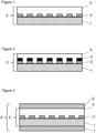
- Fig. 1 gives a schematic diagram of an example of the wiring substrate 5 according to the present invention.
- the wiring substrate 5 has a transparent substrate 1, patterned opaque wiring electrodes 2 on at least one surface of the transparent substrate 1, and a transparent protective layer 4 formed on the transparent substrate 1 and the opaque wiring electrodes 2. Each of them will be described separately below.
- the transparent substrate is transparent in the visible light region.
- a transparent material as refers to herein is one having a transmittance of 80% or more at a wavelength of 550 nm.
- the transmittance at a wavelength of 550 nm can be measured using an ultraviolet-visible spectrophotometer (U-3310, manufactured by Hitachi High-Technologies Corporation).
- the transparent substrate is, for example, a transparent substrate that is not flexible or a transparent substrate that is flexible.
- the transparent substrate that is not flexible include quartz glass, soda glass, chemically strengthened glass, Pyrex (registered trademark) glass, synthetic quartz plate, epoxy resin substrate, polyetherimide resin substrate, polyetherketone resin substrate, and polysulfone resin substrate.
- the transparent substrate that is flexible include optical resin plates and transparent films of resin such as polyethylene terephthalate film (hereinafter referred to as PET film), cycloolefin polymer film, polyimide film, polyester film, and aramid film. A plurality of these may be used in a stacked form, and for example, a plurality of transparent substrates may be used in combination after adhering them using adhesive layers.
- the surface of the transparent substrate prefferably has an inorganic film with a thickness of 5 to 50 nm.
- the inorganic film is made of silicon dioxide, niobium pentoxide, or the like. If the transparent substrate has such an inorganic film thereon, it serves to enhance the contact between the transparent substrate and the transparent protective layer. If the inorganic film has a thickness of 50 nm or less, it serves to minimize the contribution of the inorganic film to reflection. It is more preferable for the inorganic film to have a thickness of 30 nm or less. On the other hand, it is preferable for the inorganic film to have a thickness of 5 nm or more from the viewpoint of ensuring good adhesion.
- the transparent substrate may have any appropriate thickness depending on its material as long as it can support the opaque wiring electrodes stably and has a translucency as described above.
- it in order to ensure stable support of the opaque wiring electrodes, it is preferably 300 ⁇ m or more in the case of a transparent substrate of glass etc. that is not flexible and 25 ⁇ m or more in the case of a transparent substrate of PET film etc. that is flexible.
- it in order to ensure higher translucency for light used for irradiation, it is preferably 1,500 ⁇ m or less in the case of a transparent substrate of glass etc. that is not flexible and 300 ⁇ m or less in the case of a transparent substrate of PET film etc. that is flexible.
- Opaque wiring electrodes are patterned on at least one surface of the transparent substrate.
- An opaque material as refers to herein is one having a transmittance of 25% or less at a wavelength of 550 nm.
- the opaque wiring electrodes include, for example, metals such as silver, gold, copper, platinum, lead, tin, nickel, aluminum, tungsten, molybdenum, chromium, titanium, and indium, as well as alloys thereof. Of these, silver, copper, and gold are preferable from the viewpoint of electric conductivity.
- the opaque wiring electrodes may be made of a cured product of an electrically conductive composition that contains electrically conductive particles. In this case, the electrically conductive particles preferably have a spherical shape and are made of metals or alloys as described above.
- the electrically conductive particles In order to allow the electrically conductive particles to have increased dispersibility, it is preferable for the electrically conductive particles to have an average particle diameter of 0.01 ⁇ m or more, more preferably 0.03 ⁇ m or more, still more preferably 0.05 ⁇ m or more, and still more preferably 0.10 ⁇ m or more. In addition, in order to allow the opaque wiring electrodes to have sharply patterned edges, it is preferably 1.5 ⁇ m or less, and more preferably 1.0 ⁇ m or less.
- the average particle diameter of electrically conductive particles can be determined by using a scanning electron microscope (SEM) or a transmission electron microscope (TEM). They are observed at a magnification of 15,000 times, and the maximum diameters of randomly selected 100 electrically conductive particles are measured, followed by calculating their number average.
- the electrically conductive composition prefferably contains an alkali-soluble resin. If an alkali-soluble resin is included, fine opaque wiring electrodes can be formed when patterning is performed by development.
- the alkali-soluble resin include resin having a hydroxyl group and/or a carboxyl group.
- Examples of such a resin having a hydroxyl group include novolac resins having a phenolic hydroxyl group such as such as phenol novolac resin and cresol novolac resin, polymers produced from a monomer having a hydroxyl group, and copolymers produced from a monomer having a hydroxyl group and styrene, acrylonitrile, acrylic monomer, etc.
- Examples of such a monomer having a hydroxyl group include
- Examples of such a resin having a carboxyl group include carboxylic acid modified epoxy resin, carboxylic acid modified phenol resin, polyamic acid resin, carboxylic acid modified siloxane resin, polymers produced from a monomer having a carboxyl group, and copolymers produced from a monomer having carboxyl group and styrene, acrylonitrile, acrylic monomer, etc.
- Examples of such a monomer having a carboxyl group include acrylic acid, methacrylic acid, maleic acid, fumaric acid, crotonic acid, itaconic acid, citraconic acid, and cinnamic acid.
- Examples of such a resin having a hydroxyl group and a carboxyl group include copolymers produced from a monomer having a hydroxyl group and a monomer having a carboxyl group, and copolymers produced from a monomer having a hydroxyl group, a monomer having a carboxyl group, and styrene, acrylonitrile, acrylic monomer, etc. Two or more of these may be contained together.
- Such an electrically conductive composition may contain a pigment and/or a dye.
- the use of an electrically conductive composition containing a pigment and/or a dye serves to suppress the metallic luster of the opaque wiring electrodes to make the opaque wiring electrodes less visible, thereby eliminating the need to additionally provide light-shielding layers as described below.
- Light-shielding layers may be formed additionally in order to suppress more strongly the metallic luster of the opaque wiring electrodes.
- the content of the pigment and/or dye is preferably 0.5 to 2.5 mass% in the electrically conductive composition. In order to suppress the metallic luster of the opaque wiring electrodes more strongly, the content of the pigment and/or dye is preferably 0.5 mass% or more. In order to ensure an increased electric conductivity, on the other hand, the content of the pigment and/or dye is preferably 2.5 or mass% or less.
- Examples of such a pigment include lactam based pigments, perylene based pigments, phthalocyanine based pigments, isoindoline based pigments, diaminoanthraquinone based pigments, dioxazine based pigments, indanthrone based pigments, carbon black, and inorganic pigments.
- Such a dye examples include ferrocene based dyes, fluorenone based dyes, perylene based dyes, triphenyl methane based dyes, coumarin based dyes, diphenyl amine based dyes, quinacridone based dyes, quinophtharone based dyes, phthalocyanine based dyes, and xanthene based dyes.
- the electrically conductive composition prefferably be a photosensitive electrically conductive composition that further contains a photo initiator in addition to the electrically conductive particles and alkali-soluble resin described above.
- a photosensitive electrically conductive composition serves to produce fine opaque wiring electrodes by photolithography.
- photo initiator examples include 1,2-octanedione, 1-[4-(phenylthio)-2-(O-benzoyloxime)], 2,4,6-trimethylbenzoyl-diphenyl-phosphine oxide, bis(2,4,6-trimethylbenzoyl)-phenylphosphine oxide, ethanone, 1-[9-ethyl-6-2(2-methylbenzoyl)-9H-carbazole-3-yl]-1-(O-acetyloxime), benzophenone, methyl ortho-benzoylbenzoate, 4,4'-bis(dimethylamino)benzophenone, 4,4'-bis(diethylamino)benzophenone, 4,4'-dichlorobenzophenone, 4-benzoyl-4'-methyl diphenyl ketone, dibenzyl ketone, fluorenone, 2,2'-diethoxyacetophenone, 2,2-dimethoxy-2-phenyl ace
- the electrically conductive composition may further contain a dispersing agent, a monomer having an unsaturated double bond, photoacid generating agent, thermal acid generating agent, sensitizing agent, contact improving agent, surface active agent, heat curing agent, polymerization inhibitor, etc., as required.
- Examples of such a monomer having an unsaturated double bond include methyl acrylate, ethyl acrylate (hereinafter EA), acrylic acid (hereinafter AA), 2-ethylhexyl acrylate, n-butyl acrylate, i-butyl acrylate, i-propane acrylate, glycidyl acrylate, N-methoxymethyl acrylamide, N-ethoxymethyl acrylamide, N-n-butoxymethyl acrylamide, N-isobutoxymethyl acrylamide, butoxytriethylene glycol acrylate, dicyclopentanyl acrylate, dicyclopentenyl acrylate, 2-hydroxyethyl acrylate, isobornyl acrylate, 2-hydroxypropyl acrylate, isodecyl acrylate, isooctyl acrylate, lauryl acrylate, 2-methoxyethyl acrylate, methoxyethylene glycol acrylate, methoxydiethylene
- the opaque wiring electrodes have patterned shapes such as mesh-like and stripe-like.
- mesh-like shapes are preferable from the viewpoint of achieving a pattern that ensures a uniform electric conductivity.
- the opaque wiring electrodes it is more preferable for the opaque wiring electrodes to be in the form of a metal mesh that is made of a metal as described above and has a mesh-like pattern.
- a mesh shape may be, for example, in the form of an aggregation of triangular, quadrangular, polygonal, or circular units or a lattice composed of a combination of these unit shapes.
- the portions of area of containing opaque wiring electrodes preferably account for 20% or less, more preferably 15% or less, of the total area of the transparent substrate.
- Opaque wiring electrodes may be formed in two or more layers with transparent protective layers interposed in between. If opaque electrodes are formed in two layers, it serves to reduce the area of the portions that contain the opaque wiring electrodes.
- the opaque wiring electrodes From the viewpoint of electric conductivity, it is preferable for the opaque wiring electrodes to have a thickness of 0.01 ⁇ m or more, more preferably 0.05 ⁇ m or more, and still more preferably 0.1 ⁇ m or more. On the other hand, from the viewpoint of the formation of fine wiring, it is preferably for the opaque wiring electrodes to have a thickness of 10 ⁇ m or less, more preferably 5 ⁇ m or less, and still more preferably 3 ⁇ m or less.
- the opaque wiring electrodes it is preferable for the opaque wiring electrodes to have a line width of 1 to 10 ⁇ m. If the opaque wiring electrodes have a line width of 1 ⁇ m or more, it serves to increase the electric conductivity.
- the line width of the opaque wiring electrodes is more preferably 1.5 ⁇ m or more, and still more preferably 2 ⁇ m or more.
- the opaque wiring electrodes have a line width of 10 ⁇ m or less, it serves to make the opaque wiring electrodes less visible.
- the line width of the opaque wiring electrodes is more preferably 7 ⁇ m or less, and still more preferably 6 ⁇ m or less.
- the line width of the opaque wiring electrodes can be measured using an optical microscope (VHX-6000, manufactured by Keyence Corporation).
- each opaque wiring electrode 2 it is preferable for each opaque wiring electrode 2 to have a light-shielding layer 3 thereon. If a light-shielding layer is present on a opaque wiring electrode, it serves to suppress the metallic luster of the opaque wiring electrode to make the opaque wiring electrode less visible.
- the light-shielding layer may be a black film of a sputtered alloy of nickel, titanium, copper, etc., a plated film, a cured film of a resin composition containing a black pigment, or the like. Of these, the use of a cured film of a resin composition containing a black pigment is preferable from the viewpoint of the suppression of reflection in the regions containing the opaque wiring electrodes.
- the light-shielding layers may have electric conductivity, and if the light-shielding layers have electric conductivity, it serves to increase the electric conductivity of the opaque wiring electrodes.
- the opaque wiring electrodes can be formed on the surfaces of the opaque wiring electrodes by, for example, bringing the opaque wiring electrodes into contact with an aqueous hydrochloric acid solution containing palladium, tellurium, and/or their compounds.
- an aqueous hydrochloric acid solution containing palladium, tellurium, and/or their compounds it is preferable for the aqueous hydrochloric acid solution containing palladium, tellurium, and/or their compounds to have a pH of 3 or less and more preferably have a pH of 2 or less from the viewpoint of effective acceleration of plating through an oxidation-reduction reaction between the palladium and/or tellurium and the metal in the opaque wiring electrodes.
- the resin composition may contain an alkali-soluble resin, dispersing agent, monomer having an unsaturated double bond, photo initiator, photoacid generating agent, thermal acid generating agent, sensitizing agent, contact improving agent, surface active agent, heat curing agent, polymerization inhibitor, leveling agent, etc.
- an alkali-soluble resin dispersing agent, monomer having an unsaturated double bond
- photo initiator photoacid generating agent
- thermal acid generating agent thermal acid generating agent
- sensitizing agent contact improving agent
- surface active agent heat curing agent
- polymerization inhibitor leveling agent
- the resin composition containing a black pigment is preferably a positive type photosensitive resin composition that includes an alkali-soluble resin and a photoacid generating agent.
- Positive type photosensitivity as referred herein is the property of being liable to a change in the chemical structure caused by irradiation with active ray and becoming soluble in an alkali developer. If the resin composition containing a black pigment is a positive type photosensitive resin composition, light-shielding layers of the same pattern can be formed easy on opaque wiring electrodes by the method described later.
- photoacid generating agent examples include diazonium salt, diazoquinone sulfonic acid amide, diazoquinone sulfonic acid ester, diazoquinone sulfonate, nitrobenzyl ester, onium salt, halide, halogenated isocyanate, halogenated triazine, bisarylsulfonyl diazomethane, and disulfone.
- black pigment examples include organic pigments and inorganic pigments, and two or more of these pigments may be contained.
- organic pigments examples include soluble azo pigments, insoluble azo pigments, metal complex azo pigments, phthalocyanine pigments, and condensed polycyclic pigments.
- the inorganic pigments include carbon black, graphite, burnt pine, and iron oxides such as iron black, hematite, goethite, and magnetite, as well as titanium, chromium, lead, and metal composites thereof. Of these, carbon black is preferable because of being high in light shieldability.
- the black pigment preferably accounts for 5 to 30 mass% of the solid content in the resin composition. If the black pigment accounts for 5 mass% or more, it ensures a further increase in light shieldability. On the other hand, if the black pigment accounts for 30 mass% or less, it serves to increase the sensitivity to light irradiation to ensure an increased solubility.
- the content of the black pigment is more preferably 15 mass% or less. Solubility as referred to herein means the tendency of a light-irradiated portion to be dissolved in a developer, and a higher solubility suggests that the light-irradiated portion will be dissolved in a developer in a shorter period of time.
- a light-shielding layer may be formed directly on an opaque wiring electrode or may be formed on an opaque wiring electrode with a transparent protective layer interposed in between.
- the transparent protective layer is transparent in the visible light region. Transparency is defined previously.
- a sample of the transparent protective layer may be formed on a plate of non-alkali glass AN Wizus (registered trademark) (manufactured by AGC) and subjected to transmittance measurement.
- the transparent protective layer may have ion migration resistance and adhesiveness and may have a multilayer structure consisting of two or more identical or different type layers.
- it is preferably an insulation layer having ion migration resistance from the viewpoint of the prevention of short circuits from being caused by ion migration between mutually adjacent opaque wiring electrodes.
- Ion migration resistance as referred to herein means the resistance to short circuiting that can be caused by ion migration between two mutually electrically disconnected electrodes when a voltage is applied between a positive and a negative electric terminal that are connected to the electrodes.
- the transparent protective layer is an adhesive layer having adhesiveness, it can be adhered to a covering material such as cover glass and cover plastics.
- the transparent protective layer includes an insulation layer alone, it is impossible to adhere it to a covering material, whereas if it includes an adhesive layer alone, short circuiting may occur easily due to ion migration.
- both ion migration resistance and adhesiveness are ensured if an insulation layer and an adhesive layer are formed in this order on a transparent base.
- two or more opaque wiring electrode layers are formed with transparent protective layers interposed in between, it is preferable from the viewpoint of ion migration resistance to stack the same number of insulation layers as the opaque wiring electrodes. In the case where two opaque wiring electrode layers are formed with a transparent protective layer interposed in between, it is preferable to stack an insulation layer, an insulation layer, and an adhesive layer formed in this order on a transparent base.
- two or more transparent protective layers be stacked, that at least one of the transparent protective layers be an insulation layer having ion migration resistance, that at least another layer be an adhesive layer having adhesiveness, that the transparent substrate, the insulation layer, and the adhesive layer be stacked in this order, and that the refractive index n2a of the insulation layer and the refractive index n2b of the adhesive layer satisfy the equation (2) given below: 0.97 ⁇ n2a / n2b ⁇ 1 .03
- an insulating resin material such as polyimide resin, acrylic resin, cardo resin, epoxy resin, melamine resin, urethane resin, silicone based resin, and fluorine based resin, or an inorganic material such as glass. Two or more of these may be used in combination. In particular, it is preferable to adopt an insulating resin material from the viewpoint of the strength against deflection and bending of the transparent substrate.
- good materials that can be used suitably include, for example, acrylic resin, silicone resin, urethane resin, polyamide resin, polyvinyl ether resin, vinyl acetate/vinyl chloride copolymer, modified polyolefin resin, fluorine based resin, natural rubber, and synthetic rubber. Two or more of these may be used in combination.
- the transparent protective layer having adhesiveness may be a commercial product, and examples of such a commercial product include transparent adhesive films such as LUCIACS (registered trademark) CS9867US, LUCIACS (registered trademark) CS9824T, and LUCIACS (registered trademark) CS9827US (all manufactured by Nitto Denko Corporation).
- transparent adhesive films such as LUCIACS (registered trademark) CS9867US, LUCIACS (registered trademark) CS9824T, and LUCIACS (registered trademark) CS9827US (all manufactured by Nitto Denko Corporation).
- the transparent protective layer may be formed from a transparent resin composition on the transparent substrate and on the opaque wiring electrodes according to the transparent protective layer formation method described later.
- the transparent resin composition may contain an alkali-soluble resin, dispersing agent, monomer having an unsaturated double bond, photo initiator, photoacid generating agent, thermal acid generating agent, sensitizing agent, contact improving agent, surface active agent, heat curing agent, polymerization inhibitor, leveling agent, etc.
- these components those listed above in the description of the opaque wiring electrodes may be used.
- the internal reflectance R1 in the regions containing opaque wiring electrodes is 0.1% or less, and preferably 0.01% or more and 0.1% or less, as measured through the transparent protective layer. If this feature is maintained, it serves to suppress the metallic luster of the opaque wiring electrodes to make the opaque wiring electrodes less visible.
- the internal reflectance R1 can be determined as described below.
- a first substrate for reflectance evaluation is prepared as illustrated in Fig. 3 , in which an antireflection film 6 is attached to the surface of the transparent protective layer 4 in a wiring substrate 5 while a black film 7 is attached to the surface of the transparent substrate 1 in order to reduce the reflection at the interface between the transparent protective layer 4 and air and that at the interface between the transparent substrate 1 and air.
- the reflectance R3 is measured through the transparent protective layer 4.
- the reflectance R4 is measured in the same way for the region containing no opaque wiring electrode in the first substrate for reflectance evaluation 8.
- the difference R3-R4 is calculated to give the internal reflectance R1. If the internal reflectance R1 is calculated in this way, it serves to determine the internal reflectance R1 with little error because this can reduce the influence of the reflectance at the interface between the transparent protective layer 4 and air and that at the interface between the transparent substrate 1 and air even when they are significantly large. These reflectance values can be measured by using a spectrophotometer.
- Available methods for reducing the internal reflectance R1 to below 0.1% include the method of adding a pigment and/or a dye to the opaque wiring electrodes and the method of providing light-shielding layers on the opaque wiring electrodes.
- the wiring substrate according to the present invention satisfies the equation (1) given below for the refractive index n1 of the transparent substrate and the refractive index n2 of the transparent protective layer. If the refractive index n1 and the refractive index n2 satisfy the equation (1) given below, it serves to make opaque wiring electrodes less visible by suppressing the reflection at the interface between the transparent protective layer and the transparent substrate to reduce the difference between this reflection and the reflection in the regions containing the opaque wiring electrodes. 0.97 ⁇ n 2 / n1 ⁇ 1 .03
- the refractive index n1 of the transparent substrate and the refractive index n2 of the transparent protective layer can be determined by taking refractive index measurements at the wavelength of 550 nm using a prism coupler (PC-2000, manufactured by Metricon).
- PC-2000 prism coupler
- the transparent protective layer is too thin to undergo measurement alone easily, it can be determined by forming a sample of the transparent protective layer on a silicone wafer and measuring the refractive index of the transparent protective layer sample on the silicone wafer.
- the refractive index of the transparent protective layer that is in contact with the transparent substrate is adopted as n2.
- the ratio R1:R2 of the aforementioned value R1 to the reflectance R2 at the interface between the transparent protective layer and the transparent substrate is preferably in the range of 1:3 to 3:1. If R1 is so large that the ratio R1:R2 is higher than 1:3, the opaque wiring electrodes appear darker so that the opaque wiring electrodes are prevented more effectively from becoming visible. On the other hand, if R2 is so large that the ratio R1:R2 is higher than 3:1, the opaque wiring electrodes appear brighter so that the opaque wiring electrodes are prevented more effectively from becoming visible. It is more preferable for the ratio R1:R2 to be in the range of 1:2 to 2:1.
- the reflectance R2 can be calculated as described below.
- a second substrate for reflectance evaluation 9 is prepared as illustrated in Fig. 5 , in which an antireflection film 6 is attached to one surface of a transparent substrate 1 and a black film 7 is attached to the other surface of the transparent substrate 1 in order to reduce the reflection at the interface between each surface of the transparent substrate 1 and air.
- the reflectance R5 is measured through the antireflection film 6.
- the difference R4-R5 between the measured reflectance R5 and the aforementioned reflectance R4 is calculated, and this value is adopted to represent the reflectance R2 at the interface between the transparent protective layer and the transparent substrate.
- the reflectance R2 serves to determine the reflectance R2 with little error because this can reduce the influence of the reflectance at the interface between the transparent protective layer 4 and air and that at the interface between the transparent substrate 1 and air even when they are significantly large.
- the ion migration resistance of a wiring substrate can be evaluated by, for example, the method described below.
- a positive and a negative electric terminal are connected to the terminal portions of the resulting substrate for ion migration resistance evaluation and it is immersed in a constant temperature and humidity tank maintained at 85°C and 85 RH% while applying a 5 V direct current and observing the changes in electric resistance.
- the time at which the electric resistance decreases to 15,630 ⁇ is defined as the short circuiting time.
- a sample with a shorter short circuiting time is assessed as lower in ion migration resistance and a sample with a longer short circuiting time is assessed as higher in ion migration resistance.
- Figs. 6 to 9 and Fig. 12 give schematic diagrams of other examples of the wiring substrate according to the present invention.
- Fig. 6 gives a schematic diagram of a wiring substrate including a transparent substrate 1, first opaque wiring electrodes 2 disposed thereon, a first transparent protective layer 4 disposed on the first opaque wiring electrodes 2, and second opaque wiring electrodes 2 and a second transparent protective layer 4 disposed on the first transparent protective layer 4.
- Fig. 7 gives a schematic diagram of a wiring substrate including a transparent substrate 1, first opaque wiring electrodes 2 disposed thereon, a first transparent protective layer 4 disposed on the first opaque wiring electrodes 2, second opaque wiring electrodes 2 disposed on the first transparent protective layer 4, and light-shielding layers 3 and a second transparent protective layer 4 disposed on the second opaque wiring electrodes 2.
- Fig. 8 gives a schematic diagram of a wiring substrate including a transparent substrate 1, opaque wiring electrodes 2 disposed on both surfaces thereof, and transparent protective layers 4 disposed on the opaque wiring electrodes 2 on both surfaces of the transparent substrate 1.
- Fig. 9 gives a schematic diagram of a wiring substrate including a transparent substrate 1, opaque wiring electrodes 2 disposed on both surfaces thereof, light-shielding layers 3 disposed on the opaque wiring electrodes 2 on one surface thereof, and transparent protective layers 4 disposed on the opaque wiring electrodes 2 and the light-shielding layers 3 on both surfaces of the transparent substrate 1.
- Fig. 12 gives a schematic diagram of a wiring substrate including a transparent substrate 1, opaque wiring electrodes 2 disposed on one surface thereof, a first transparent protective layer 4 disposed on the opaque wiring electrodes 2, and a second transparent protective layer 4 disposed on the first transparent protective layer 4.
- opaque wiring electrodes are formed on at least one surface of a transparent substrate. These opaque wiring electrodes may be formed on both surfaces of a transparent substrate.
- the process for forming opaque wiring electrodes on at least one surface of a transparent substrate may include a step for forming first opaque wiring electrodes on one surface of a transparent substrate, a step for forming a transparent protective layer on the first opaque wiring electrodes, and a step for forming second opaque wiring electrodes on the transparent protective layer.
- opaque wiring electrodes include, for example, a method designed to perform pattern formation by photolithography using a photosensitive electrically conductive composition as described above, a method designed to perform pattern formation by screen printing, gravure printing, ink jet printing, etc., using an electrically conductive composition (electrically conductive paste), and a method designed to first form a film of a metal, metal composite, metal-metal compound composite, metal alloy, etc., and perform pattern formation by photolithography using a resist.
- the use of a method designed to perform pattern formation by photolithography using a photosensitive electrically conductive composition is preferable because it can serve to produce fine wiring.
- the opaque wiring electrodes may be formed either by the same method or by different methods in combination.
- Such a method that performs pattern formation by photolithography using a photosensitive electrically conductive composition includes a coating step for coating a transparent substrate with a photosensitive electrically conductive composition to form a coating film, a photolithography step for performing light irradiation and development of the coating film to form a pattern, and a curing step for heating the pattern at 100°C to 300°C to produce an electrically conductive pattern.
- a photosensitive electrically conductive composition as described above is spread over a transparent substrate to form a coating film.
- Good methods for spreading a photosensitive electrically conductive composition over a transparent substrate include, for example, spin coating with a spinner, spray coating, roll coating, screen printing, and the use of a slit coater, blade coater, die coater, calender coater, meniscus coater, or bar coater.
- the resulting coating film may be dried to remove the solvent.
- Good methods for drying the coating film include, for example, heat drying by an oven, hot plate, or infrared ray irradiation, and vacuum drying. Heat drying is generally performed at a temperature of 50°C to 120°C for a heat drying time of 1 minute to several hours.
- the coating film prepared in the coating step is irradiated with light and developed to form a pattern.
- Preferable light sources for the light irradiation of a coating film include the i-line (365 nm), h-line (405 nm), and g-line (436 nm) of a mercury lamp or LED lamp.
- Light is applied through a light irradiation mask to the surface of the transparent substrate that is coated with a photosensitive electrically conductive composition, and then non-irradiated portions are removed with a developer to produce an electrically conductive pattern.
- Examples of useful developers to perform alkali development include aqueous solutions of tetramethyl ammonium hydroxide, diethanol amine, diethyl aminoethanol, sodium hydroxide, potassium hydroxide, sodium carbonate, potassium carbonate, triethyl amine, diethyl amine, methyl amine, dimethyl amine, dimethylaminoethyl acetate, dimethylaminoethanol, dimethylaminoethyl methacrylate, cyclohexyl amine, ethylene diamine, and hexamethylene diamine, and these aqueous solutions may contain polar solvents such as N-methyl-2-pyrrolidone, N,N-dimethyl formamide, N,N-dimethyl acetamide, dimethyl sulfoxide, and ⁇ -butyrolactone, alcohols such as methanol, ethanol, and isopropanol, esters such as ethyl lactate and propylene glycol monomethyl ether acetate, and keto
- Examples of useful developers for organic development include polar solvents such as N-methyl-2-pyrrolidone, N-acetyl-2-pyrrolidone, N,N-dimethyl acetamide, N,N-dimethyl formamide, dimethyl sulfoxide, hexamethylphosphoric riamide, and mixed solutions of these polar solvents with methanol, ethanol, isopropyl alcohol, xylene, water, methyl carbitol, or ethyl carbitol.
- polar solvents such as N-methyl-2-pyrrolidone, N-acetyl-2-pyrrolidone, N,N-dimethyl acetamide, N,N-dimethyl formamide, dimethyl sulfoxide, hexamethylphosphoric riamide, and mixed solutions of these polar solvents with methanol, ethanol, isopropyl alcohol, xylene, water, methyl carbitol, or ethyl carbitol.
- Good development methods include, for example, the technique of spraying a developer over the surface of a coated film on a stationary or rotating substrate, the technique of immersing a substrate in a developer, and the technique of applying ultrasonic waves to a substrate immersed in a developer.
- the pattern formed in the development step may be rinsed with a rinsing liquid.
- a rinsing liquid examples include water and aqueous solutions prepared by adding alcohols such as ethanol and isopropyl alcohol, esters such as ethyl lactate and propylene glycol monomethyl ether acetate, or surface active agents to water.
- light-shielding layers having the same pattern as the opaque wiring electrodes can be formed by first forming opaque wiring electrodes on a transparent base, coating them with a positive type photosensitive resin composition containing a black pigment, then irradiating the positive type photosensitive resin composition containing a black pigment with light applied through the opposite uncoated surface utilizing the opaque wiring electrodes as mask, followed by carrying out development.
- a light-shielding layer has to be removed from particular portions, such as terminal portions, to expose the opaque wiring electrode in order to provide electric connection to external devices, it may be good to add a step, as required, for applying light to the surface coated with the positive type photosensitive resin composition using a light irradiation mask.
- the process for producing the light-shielding layers may include a curing step.
- the curing temperature is preferably 100°C to 300°C.
- Good curing techniques include, for example, heat drying by an oven, inert oven, or hot plate, heat drying by an infrared ray heater or other electromagnetic wave generation devices, and vacuum drying.
- a transparent protective layer is formed on the transparent substrate and opaque wiring electrodes.
- Good methods for forming a transparent protective layer include, for example, the technique of spreading and subsequently drying a transparent resin composition and the technique of attaching a transparent adhesive film to the surface having opaque wiring electrodes thereon.
- Good methods for spreading a transparent resin composition include, for example, spin coating with a spinner, spray coating, roll coating, screen printing, offset printing, gravure printing, typographic printing, flexographic printing, and the use of a blade coater, die coater, calender coater, meniscus coater, or bar coater.
- the dried film may be cured by ultraviolet ray treatment and/or heat treatment.
- the transparent resin composition may have photosensitivity.
- a transparent protective layer has to be removed from particular portions, such as terminal portions, to expose the opaque wiring electrode in order to provide electric connection to external devices, it may be good to adopt a photolithography step for its removal as in the case of the photosensitive electric conductive composition.
- the transmittance of a transparent substrate at a wavelength of 550 nm was measured using an ultraviolet-visible spectrophotometer (U-3310, manufactured by Hitachi High-Technologies Corporation).
- the refractive index at a wavelength of 550 nm was measured using a prism coupler (PC-2000, manufactured by Metricon) at room temperature of 23°C.
- DMEA diethylene glycol monoethyl ether acetate
- 2-EHMA 2- ethylhexyl methacrylate
- St styrene
- a 25.0 g amount of 36 mass% hydrochloric acid and 0.5 g of tellurium dioxide were mixed in water and, after complete dissolution of tellurium dioxide, 10.0 g of acetic acid and 64.5 g of water were added, followed by mixing them to provide 100.0 g of an aqueous solution with a pH of 0 designed to blacken electrodes.
- the pH value was measured using a pH meter (AP-20, manufactured by A&D Company, Limited) at a temperature of 25°C.
- the resulting photosensitive insulation paste (E-6) was spread over a 4 inch silicone wafer and the refractive index at a wavelength of 550 nm was measured at room temperature of 23°C using a prism coupler (PC-2000, manufactured by Metricon). Results showed that it was 1.66.
- the adhesive agent composition was spread over a release film and dried at 100°C for 2 minutes to form an adhesive layer with a thickness of 25 ⁇ m, and then a release film was attached to the adhesive layer to produce a transparent adhesive film (b-2).
- the refractive index at a wavelength of 550 nm of the resulting transparent adhesive film was measured and results showed that it was 1.51.
- a black film was attached to the opposite surface to the one having opaque wiring electrodes and then, while applying light to the wiring substrate using a floodlight projector, 10 testers observed it visually from a position 30 cm away and determined if the mesh-like electrode portion was visible.
- a sample was rated as E if it was visible for 8 or more testers, rated as D if it was visible for 5 or more and less than 8 testers, rated as C if it was visible for 3 or more and less than 5 testers, rated as B if it was visible for 1 or more and less than 3 testers, and rated as A if it was invisible for the 10 testers, and assessed as acceptable if rated as D or higher.
- an antireflection film was attached to the surface of the transparent protective layer using a rubber roller in order to suppress reflection at the interface between the transparent protective layer and air.
- a black film was attached to the surface of the transparent substrate using a rubber roller in order to suppress reflection at the interface between the transparent substrate and air, thereby preparing a first substrate for reflectance evaluation as illustrated in Fig. 3 .
- the reflectance R3 was measured through the transparent protective layer.
- the reflectance R4 was measured in the same way for the regions containing no opaque wiring electrodes in the first substrate for reflectance evaluation.
- the reflectances R3 and R4 were determined by a spectrophotometer (CM-2500d, manufactured by Konica Minolta Sensing, Inc.) by measuring the luminous reflectance (Y value) under the conditions of a D65 light source and a field of view of 10°.
- CM-2500d manufactured by Konica Minolta Sensing, Inc.
- an antireflection film was attached to one surface of the transparent substrate using a rubber roller. Furthermore, a black film was attached to the other surface of the transparent substrate using a rubber roller to prepare a second substrate for reflectance evaluation as illustrated in Fig. 5 .
- the reflectance R5 was measured through the antireflection film. From the measured reflectance R5 and reflectance R4, the difference R4-R5 was calculated to give the reflectance R2.
- the reflectance R5 was determined by a spectrophotometer (CM-2500d, manufactured by Konica Minolta Sensing, Inc.) by measuring the luminous reflectance (Y value) under the conditions of a D65 light source and a field of view of 10°.
- CM-2500d manufactured by Konica Minolta Sensing, Inc.
- the difference R3-R5 was calculated from the measured reflectance R5 and reflectance R3 to give the reflectance R in the regions containing opaque wiring electrodes.
- a sample was rated as A if the reflectance R was less than 0.12%, rated as B if it was 0.12% or more and less than 0.16%, rated as C if it was 0.16% or more and less than 0.26%, and rated as D if it was 0.26% or more.
- a positive and a negative electric terminal were connected to the terminal portions and it was immersed in a constant temperature and humidity tank maintained at 85°C and 85 RH% while applying a 5 V direct current and measuring the changes in electric resistance.
- the time at which the electric resistance decreased to 15,630 ⁇ was defined as the short circuiting time, and a sample was rated as A if the short circuiting time was 500 hours or more, rated as B if it was less than 500 hours and 100 hours or more, and rated as C if it was less than 100 hours.
- a PET film was attached to one surface of the transparent protective layer using a rubber roller, and the adhesive strength was measured using an adhered and coated film peeling analysis instrument (VPA, manufactured by Kyowa Interface Science Co., Ltd.) under the conditions of a peeling speed of 300 mm/min and a peeling angle of 180°.
- a sample was rated as A if the adhesive strength was 3.0 N/25 mm or more and rated as B if the adhesive strength was less than 3.0 N/25 mm.
- the regions containing opaque wiring electrodes were subjected to contact test according to the crosscut method specified in JIS K 5600-5-6: 1999. A sample was rated as A if it fell under class 0, rated as B if it fell under class 1 or 2, and rated as C if it fell under any of classes 3 to 5.
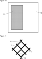
- the photosensitive electrically conductive paste (D-1) prepared in Production example 3 was spread over one surface of the transparent substrate (a-1) by spin coating so that it would have a thickness of 1 ⁇ m after drying, and then it was dried at 90°C for 8 minutes. Then, as illustrated in Fig. 10 and Fig. 11 , it was irradiated with a light exposure of 100 mJ/cm 2 (converted for wavelength 365 nm) through a light irradiation mask having a mask mesh portion of a mesh shape with a mesh pitch of 150 ⁇ m and a mesh angle of 90° and a mask shielding portion using a light irradiation instrument (PEM-6M, manufactured by Union Optical Co., Ltd.).
- PEM-6M light irradiation instrument
- the mask aperture width was 4 ⁇ m. Subsequently, using a 0.1% aqueous solution of tetramethyl ammonium hydroxide as developer, it was subjected to development for a period twice as long as the time required for dissolving the light-irradiated portion, rinsed with ultrapure water for 30 seconds, and heated in a box oven at 240°C for 60 minutes to provide a substrate having opaque wiring electrodes. The resulting opaque wiring electrodes were observed under an optical microscope and consequently found to have a line width of 4 ⁇ m.
- the surface having opaque wiring electrodes thereon was coated with the light-shielding paste prepared in Production example 6 by spin coating so as to form light-shielding layers with a thickness of 0.5 ⁇ m after drying, and it was dried at 80°C for 5 minutes. Then, it was irradiated with a light exposure of 500 mJ/cm 2 (converted for wavelength 365 nm) using the opaque wiring electrodes as mask through the surface opposite to the one having opaque wiring electrodes. Subsequently, using a 2.38% aqueous solution of tetramethyl ammonium hydroxide as developer, it was subjected to immersion development for 50 seconds to form light-shielding layers on the opaque wiring electrodes. In addition, it was heated in a box oven at 240°C for 60 minutes to provide a substrate having light-shielding layers.
- the surface having opaque wiring electrodes and light-shielding layers was coated with the photosensitive electrically insulating paste (E-1) prepared in Production example 8 by spin coating so as to from a film that would have a thickness of 1.5 ⁇ m after drying, and then it was dried at 80°C for 5 minutes. Subsequently, it was irradiated with a light exposure of 100 mJ/cm 2 (converted for wavelength 365 nm) through a light irradiation mask using a light irradiation instrument (PEM-6M, manufactured by Union Optical Co., Ltd.).
- PEM-6M light irradiation instrument
- first wiring substrate was subjected to visibility evaluation, reflectance R1 measurement, evaluation of reflectance R in the regions containing opaque wiring electrodes, adhesiveness evaluation, and contact evaluation.
- Example 1 Except for adopting the transparent substrate, the photosensitive insulation paste for transparent protective layer formation, and the light irradiation mask pattern for opaque wiring electrode formation that are specified in Table 1, the same procedure as in Example 1 was carried out to produce a first wiring substrate and a second wiring substrate as illustrated in Fig. 2 .
- Example 2 Except for adopting the photosensitive electrically conductive paste (D-2) instead of the photosensitive electrically conductive paste (D-1) and also adopting a pattern having a mesh shape with a pitch of 450 ⁇ m and an angle of 90° along with a mask aperture width of 12 ⁇ m, the same procedure as for the ⁇ Formation of opaque wiring electrode> in Example 1 was carried out to produce a substrate having opaque wiring electrodes. The resulting opaque wiring electrodes were observed under an optical microscope and consequently found to have a line width of 12 ⁇ m.
- Example 2 For the resulting substrate having opaque wiring electrodes, the same procedure as for the ⁇ Formation of transparent protective layer> in Example 1 was carried out to form a transparent protective layer on the surface having opaque wiring electrodes to produce a first wiring substrate as illustrated in Fig. 1 .
- Example 8 Except for adopting the photosensitive insulation paste for transparent protective layer formation that is specified in Table 1, the same procedure as in Example 8 was carried out to produce a first wiring substrate and a second wiring substrate as illustrated in Fig. 1 .
- Example 2 Except for using a pattern having a mesh shape with a pitch of 450 ⁇ m and an angle of 90° along with a mask aperture width of 12 ⁇ m, the same procedure as in Example 1 was carried out to produce a substrate having opaque wiring electrodes.
- the opaque wiring electrodes were observed under an optical microscope and consequently found to have a line width of 12 ⁇ m.
- the resulting substrate having opaque wiring electrodes was immersed in the aqueous solution for blackening electrodes prepared in Production example 7 for 30 seconds, then rinsed with water, and dried to produce a substrate having light-shielding layers in which light-shielding layers were disposed on the surfaces of the opaque wiring electrodes.
- Example 2 For the resulting substrate having light-shielding layers, except for adopting the photosensitive insulation paste (E-3) instead of the photosensitive insulation paste (E-1), the same procedure as in Example 1 was carried out to produce a transparent protective layer on the surface having opaque wiring electrodes and light-shielding layers formed thereon, thereby providing a first wiring substrate as illustrated in Fig. 2 .
- Example 2 Except for using a pattern having a mesh shape with a pitch of 300 ⁇ m and an angle of 90°, the same procedure as in Example 1 was carried out to produce a substrate having opaque wiring electrodes (referred to below as the first opaque wiring electrodes in this Example).
- the first opaque wiring electrodes were observed under an optical microscope and consequently found to have a line width of 4 ⁇ m.
- Example 3 For the resulting substrate having the first opaque wiring electrodes, except for adopting the photosensitive insulation paste (E-3) instead of the photosensitive insulation paste (E-1), the same procedure as for the ⁇ Formation of transparent protective layer> in Example 1 was carried out to produce a transparent protective layer (referred to below as the first transparent protective layer in this Example) to cover the surface having the first opaque wiring electrodes formed thereon, thereby providing a substrate having the first transparent protective layer.
- a transparent protective layer referred to below as the first transparent protective layer in this Example
- the same procedure as for the formation of the first opaque wiring electrodes was carried out to produce second opaque wiring electrodes on the surface having the first transparent protective layer formed thereon to produce a substrate having the second opaque wiring electrodes.
- the second opaque wiring electrodes were observed under an optical microscope and consequently found to have a line width of 4 ⁇ m.
- Example 2 For the resulting substrate having the second opaque wiring electrodes, the same procedure as for the ⁇ Formation of light-shielding layer> in Example 1 was carried out to form light-shielding layers on the surface having the second opaque wiring electrodes formed thereon in such a manner that they were disposed at the positions corresponding to the opaque wiring electrodes. In addition, it was heated in a box oven at 240°C for 60 minutes to provide a substrate having light-shielding layers.
- the same procedure as for the ⁇ Formation of first transparent protective layer> was carried out to form a second transparent protective layer on the surface having opaque wiring electrodes and light-shielding layers formed thereon to provide a wiring substrate as illustrated in Fig. 7 .
- Example 2 Except for adopting the transparent substrate (a-2) instead of the transparent substrate (a-1) and using a pattern having a mesh shape with a pitch of 300 ⁇ m and an angle of 90° along with a mask aperture width of 4 ⁇ m, the same procedure as for the ⁇ Formation of opaque wiring electrode> in Example 1 was carried out to produce a substrate having the first opaque wiring electrodes. The resulting first opaque wiring electrodes were observed under an optical microscope and consequently found to have a line width of 4 ⁇ m.
- the same procedure as for the formation of the first opaque wiring electrodes was carried out to produce second opaque wiring electrodes on the opposite surface to the one having the first opaque wiring electrodes formed thereon to produce a substrate having second opaque wiring electrodes.
- the second opaque wiring electrodes were observed under an optical microscope and consequently found to have a line width of 4 ⁇ m.
- the same procedure as for the ⁇ Formation of light-shielding layer> in Example 1 except for adopting a light exposure of 3,000 mJ/cm 2 was carried out to form light-shielding layers on the surface having the first opaque wiring electrodes formed thereon in such a manner that they were disposed at the positions corresponding to the opaque wiring electrodes.
- it was heated in a box oven at 240°C for 60 minutes to provide a substrate having light-shielding layers.
- Example 2 For the resulting substrate having light-shielding layers, the same procedure as for the ⁇ Formation of transparent protective layer> in Example 1 except for adopting the photosensitive insulation paste (E-6) instead of the photosensitive insulation paste (E-1) was carried out to produce a first transparent protective layer on the surface having the first opaque wiring electrodes and light-shielding layers formed thereon, thereby providing a substrate having the first transparent protective layer.
- the photosensitive insulation paste (E-6) instead of the photosensitive insulation paste (E-1) was carried out to produce a first transparent protective layer on the surface having the first opaque wiring electrodes and light-shielding layers formed thereon, thereby providing a substrate having the first transparent protective layer.
- Example 2 Except for sputtering a 1 ⁇ m thick layer of silicon dioxide on one surface of the transparent substrate (a-1) using a sputtering machine, the same procedure as in Example 1 was carried out to produce a first wiring substrate and a second wiring substrate as illustrated in Fig. 2 .
- Example 13 Except for forming a silicon dioxide layer with a thickness as specified in Table 2, the same procedure as in Example 13 was carried out to produce a first wiring substrate and a second wiring substrate as illustrated in Fig. 2 .
- Example 14 The same procedure as in Example 14 was carried out to produce a substrate having opaque wiring electrodes.
- the resulting first opaque wiring electrodes were observed under an optical microscope and consequently found to have a line width of 4 ⁇ m.
- Example 2 For the resulting substrate having opaque wiring electrodes, the same procedure as in Example 1 was carried out on the surface having opaque wiring electrodes formed thereon to produce a substrate having light-shielding layers.
- a transparent adhesive film (b-1) was attached using a rubber roller to form a second transparent protective layer on the surface having the first transparent protective layer formed thereon to provide a first wiring substrate as illustrated in Fig. 12 .
- a light irradiation mask having a line width of 10 ⁇ m and a line space of 10 ⁇ m as illustrated in Fig. 13 was adopted for the ⁇ Formation of opaque wiring electrode>, that after light irradiation for the ⁇ Formation of light-shielding layer>, only the wiring portions were light-shielded, followed by re-irradiation through the film surface with a light exposure of 500 mJ/cm 2 (converted for wavelength 365 nm), that the terminal portions were light-shielded when performing light irradiation for the ⁇ Formation of first transparent protective layer>, and that in the ⁇ Formation of second transparent protective layer>, a transparent adhesive film (b-1) was attached using a rubber roller to only the wiring portion of the surface having the first transparent protective layer formed thereon, the same procedure as for producing the first wiring substrate was carried out to produce a second wiring substrate.
- Example 18 Except for adopting the second transparent protective layer (b-2) instead of (b-1), the same procedure as in Example 18 was carried out to produce a first wiring substrate and a second wiring substrate as illustrated in Fig. 12 .
- Example 14 The same procedure as for the ⁇ Formation of opaque wiring electrode> under [Preparation of first wiring substrate] in Example 14 was carried out to produce a substrate having opaque wiring electrodes.
- the resulting first opaque wiring electrodes were observed under an optical microscope and consequently found to have a line width of 4 ⁇ m.
- Example 14 For the resulting substrate having opaque wiring electrodes, the same procedure as for the ⁇ Formation of light-shielding layer> in Example 14 was carried out on the surface having opaque wiring electrodes formed thereon to produce a substrate having light-shielding layers.
- a transparent adhesive film (b-2) was attached using a rubber roller to the surface having light-shielding layers formed thereon to form a transparent protective layer, thereby providing a first wiring substrate as illustrated in Fig. 2 .
- a light irradiation mask having a line width of 10 ⁇ m and a line space of 10 ⁇ m as illustrated in Fig. 13 was adopted for the ⁇ Formation of opaque wiring electrode>, that after light irradiation for the ⁇ Formation of light-shielding layer>, only the wiring portions were light-shielded, followed by re-irradiation through the film surface with a light exposure of 500 mJ/cm 2 (converted for wavelength 365 nm), and that in the ⁇ Formation of transparent protective layer>, a transparent adhesive film (b-2) was attached using a rubber roller to only the wiring portion of the surface having light-shielding layers formed thereon, the same procedure as for producing the first wiring substrate was carried out to produce a second wiring substrate.
- Example 8 Except for adopting the photosensitive insulation paste specified in Table 3 to form opaque wiring electrodes, the same procedure as in Example 8 was carried out to produce a first wiring substrate and a second wiring substrate as illustrated in Fig. 1 .
- Example 3 Except for adopting the transparent substrate and the photosensitive insulation paste for transparent protective layer formation that are specified in Table 3, the same procedure as in Example 1 was carried out to produce a first wiring substrate and a second wiring substrate as illustrated in Fig. 2 .
- Example 1 Example 2
- Example 3 Example 4
- Example 5 Example 6
- Example 7 Example 8
- Example 10 transparent substrate substrate a-1 a-1 a-1 a-2 a-1 a-1 a-1 a-1 a-1 a-1 refractive index n1 1.52 1.52 1.52 1.68 1.52 1.52 1.52 1.52 1.52 1.52 1.52 thickness of inorganic film - - - - - - - opaque wiring electrode photosensitive electrically conductive paste D-1 D-1 D-1 D-1 D-1 D-1 D-1 D-2 D-2 D-1 line width ( ⁇ m) 4 4 4 8 6 12 12 12 12 12 pitch ( ⁇ m) 150 150 150 150 150 150 150 150 150 150 90 150 450 450 450 thickness of light-shielding layer ( ⁇ m) 0.5 0.5 0.5 0.5 0.5 0.5 0.5 0.5 0.5 0.5 - - ⁇ 0.1 transparent protective layer photosensitive insulation paste E-1 E-2 E-3 E-6 E-1 E-3 E-1 E-1 E-3 E-3 E-3 refractive index n2
- Example 11 Example 12
- Example 13 Example 14
- Example 15 Example 16
- Example 17 Example 18
- Example 20 transparent substrate substrate a-1 a-2 a-1 a-1 a-1 a-1 a-1 a-1 a-1 a-1 a-1 a-1 refractive index n1 1.52 1.68 1.52 1.52 1.52 1.52 1.52 1.52 1.52 1.52 1.52 1.52 1.52 thickness of inorganic film (nm) - - 1 10
- 30 10
- 10 opaque wiring electrode photosensitive electrically conductive paste
- 300 150 150 150 150 150 150 150 150 150 150 150 150 150 150 150 150 150 150 150 150 150 150 150 thickness of light-shielding layer ( ⁇ m) 0.5 0.5 0.5 0.5 0.5 0.5 0.5 0.5 transparent protective layer photosensitive insulation paste E-3
Landscapes
- Engineering & Computer Science (AREA)
- Microelectronics & Electronic Packaging (AREA)
- General Engineering & Computer Science (AREA)
- Theoretical Computer Science (AREA)
- Manufacturing & Machinery (AREA)
- Human Computer Interaction (AREA)
- Physics & Mathematics (AREA)
- General Physics & Mathematics (AREA)
- Laminated Bodies (AREA)
- Non-Insulated Conductors (AREA)
Applications Claiming Priority (3)
| Application Number | Priority Date | Filing Date | Title |
|---|---|---|---|
| JP2020207270 | 2020-12-15 | ||
| JP2021134669 | 2021-08-20 | ||
| PCT/JP2021/040014 WO2022130803A1 (ja) | 2020-12-15 | 2021-10-29 | 配線基板 |
Publications (2)
| Publication Number | Publication Date |
|---|---|
| EP4266840A1 true EP4266840A1 (de) | 2023-10-25 |
| EP4266840A4 EP4266840A4 (de) | 2024-11-20 |
Family
ID=82059756
Family Applications (1)
| Application Number | Title | Priority Date | Filing Date |
|---|---|---|---|
| EP21906167.8A Pending EP4266840A4 (de) | 2020-12-15 | 2021-10-29 | Leiterplatte |
Country Status (4)
| Country | Link |
|---|---|
| US (1) | US12349269B2 (de) |
| EP (1) | EP4266840A4 (de) |
| JP (1) | JP7729208B2 (de) |
| WO (1) | WO2022130803A1 (de) |
Families Citing this family (1)
| Publication number | Priority date | Publication date | Assignee | Title |
|---|---|---|---|---|
| CN119895367A (zh) * | 2022-12-20 | 2025-04-25 | 东丽株式会社 | 布线基板、遮光层形成用正型感光性树脂组合物、遮光层转印膜及布线基板的制造方法 |
Family Cites Families (11)
| Publication number | Priority date | Publication date | Assignee | Title |
|---|---|---|---|---|
| JP4197572B2 (ja) * | 2000-05-12 | 2008-12-17 | 日東電工株式会社 | 反射型液晶表示装置 |
| JP4667471B2 (ja) * | 2007-01-18 | 2011-04-13 | 日東電工株式会社 | 透明導電性フィルム、その製造方法及びそれを備えたタッチパネル |
| JP2010086684A (ja) * | 2008-09-30 | 2010-04-15 | Kuramoto Seisakusho Co Ltd | 透明導電配線膜付き光学薄膜 |
| JP6324656B2 (ja) * | 2012-07-12 | 2018-05-16 | 大日本印刷株式会社 | タッチパネル基板、及び表示装置 |
| KR102029439B1 (ko) | 2012-12-07 | 2019-11-08 | 엘지디스플레이 주식회사 | 터치 스크린 패널용 투명 평면체 및 이를 포함하는 터치 스크린 패널 |
| WO2014203418A1 (ja) | 2013-06-19 | 2014-12-24 | 凸版印刷株式会社 | 表示装置用基板および表示装置 |
| JP2015097039A (ja) | 2013-11-15 | 2015-05-21 | 富士フイルム株式会社 | 導電性フィルム、これを備えるタッチパネル及び表示装置、並びに配線の視認性の評価方法 |
| JP6253448B2 (ja) | 2014-02-25 | 2017-12-27 | 富士フイルム株式会社 | 導電性フィルムシート |
| JP6231432B2 (ja) * | 2014-05-02 | 2017-11-15 | 富士フイルム株式会社 | 導電性フイルム、それを備える表示装置及び導電性フイルムの評価方法 |
| JP6717053B2 (ja) * | 2016-05-25 | 2020-07-01 | 凸版印刷株式会社 | 配線基板、タッチパネル、カラーフィルタ基板、及び表示装置 |
| WO2018168325A1 (ja) | 2017-03-17 | 2018-09-20 | 東レ株式会社 | 配線電極付き基板の製造方法および配線電極付き基板 |
-
2021
- 2021-10-29 EP EP21906167.8A patent/EP4266840A4/de active Pending
- 2021-10-29 JP JP2021569091A patent/JP7729208B2/ja active Active
- 2021-10-29 WO PCT/JP2021/040014 patent/WO2022130803A1/ja not_active Ceased
- 2021-10-29 US US18/030,828 patent/US12349269B2/en active Active
Also Published As
| Publication number | Publication date |
|---|---|
| EP4266840A4 (de) | 2024-11-20 |
| WO2022130803A1 (ja) | 2022-06-23 |
| US20230309217A1 (en) | 2023-09-28 |
| JPWO2022130803A1 (de) | 2022-06-23 |
| JP7729208B2 (ja) | 2025-08-26 |
| US12349269B2 (en) | 2025-07-01 |
Similar Documents
| Publication | Publication Date | Title |
|---|---|---|
| JP5967079B2 (ja) | 導電ペーストおよび導電パターンの製造方法 | |
| WO2011114846A1 (ja) | 感光性導電ペーストおよび導電パターンの製造方法 | |
| KR101898955B1 (ko) | 도전 패턴 형성 부재의 제조 방법 | |
| TWI733001B (zh) | 附有配線電極之基板的製造方法 | |
| US12349269B2 (en) | Wiring board | |
| JP5764931B2 (ja) | 有機−無機複合導電性パターン形成用感光性ペーストおよび有機−無機複合導電性パターンの製造方法 | |
| CN106463199B (zh) | 导电糊剂、触控面板和导电图案的制造方法 | |
| KR20160062002A (ko) | 감광성 차광 페이스트 및 터치 센서용 적층 패턴의 제조 방법 | |
| US9846362B2 (en) | Conductive paste and method of producing conductive pattern | |
| US20160313833A1 (en) | Method of producing touch sensor member, and touch sensor member | |
| JP2013195733A (ja) | 感光性導電ペースト | |
| CN116602061A (zh) | 布线基板 | |
| US9081278B2 (en) | Photosensitive conductive paste and method of producing conductive pattern | |
| JP6729378B2 (ja) | 導電ペースト、タッチセンサー部材及び導電パターンの製造方法 | |
| JP6717439B1 (ja) | 積層部材 | |
| WO2024004318A1 (ja) | 配線電極付き基板の製造方法 | |
| WO2018029749A1 (ja) | 導電パターン形成部材の製造方法 |
Legal Events
| Date | Code | Title | Description |
|---|---|---|---|
| STAA | Information on the status of an ep patent application or granted ep patent |
Free format text: STATUS: THE INTERNATIONAL PUBLICATION HAS BEEN MADE |
|
| PUAI | Public reference made under article 153(3) epc to a published international application that has entered the european phase |
Free format text: ORIGINAL CODE: 0009012 |
|
| STAA | Information on the status of an ep patent application or granted ep patent |
Free format text: STATUS: REQUEST FOR EXAMINATION WAS MADE |
|
| 17P | Request for examination filed |
Effective date: 20230524 |
|
| AK | Designated contracting states |
Kind code of ref document: A1 Designated state(s): AL AT BE BG CH CY CZ DE DK EE ES FI FR GB GR HR HU IE IS IT LI LT LU LV MC MK MT NL NO PL PT RO RS SE SI SK SM TR |
|
| DAV | Request for validation of the european patent (deleted) | ||
| DAX | Request for extension of the european patent (deleted) | ||
| A4 | Supplementary search report drawn up and despatched |
Effective date: 20241018 |
|
| RIC1 | Information provided on ipc code assigned before grant |
Ipc: G06F 3/044 20060101ALI20241014BHEP Ipc: G06F 3/041 20060101ALI20241014BHEP Ipc: H05K 3/28 20060101AFI20241014BHEP |
|
| STAA | Information on the status of an ep patent application or granted ep patent |
Free format text: STATUS: EXAMINATION IS IN PROGRESS |
|
| 17Q | First examination report despatched |
Effective date: 20251020 |