EP4268290B1 - Procédé de gravure sélective d'un composant métallique - Google Patents
Procédé de gravure sélective d'un composant métallique Download PDFInfo
- Publication number
- EP4268290B1 EP4268290B1 EP20838103.8A EP20838103A EP4268290B1 EP 4268290 B1 EP4268290 B1 EP 4268290B1 EP 20838103 A EP20838103 A EP 20838103A EP 4268290 B1 EP4268290 B1 EP 4268290B1
- Authority
- EP
- European Patent Office
- Prior art keywords
- metal
- metal component
- hard mask
- component
- semiconductor component
- Prior art date
- Legal status (The legal status is an assumption and is not a legal conclusion. Google has not performed a legal analysis and makes no representation as to the accuracy of the status listed.)
- Active
Links
Images


Classifications
-
- H—ELECTRICITY
- H10—SEMICONDUCTOR DEVICES; ELECTRIC SOLID-STATE DEVICES NOT OTHERWISE PROVIDED FOR
- H10N—ELECTRIC SOLID-STATE DEVICES NOT OTHERWISE PROVIDED FOR
- H10N60/00—Superconducting devices
- H10N60/01—Manufacture or treatment
-
- H—ELECTRICITY
- H10—SEMICONDUCTOR DEVICES; ELECTRIC SOLID-STATE DEVICES NOT OTHERWISE PROVIDED FOR
- H10P—GENERIC PROCESSES OR APPARATUS FOR THE MANUFACTURE OR TREATMENT OF DEVICES COVERED BY CLASS H10
- H10P50/00—Etching of wafers, substrates or parts of devices
- H10P50/71—Etching of wafers, substrates or parts of devices using masks for conductive or resistive materials
-
- H—ELECTRICITY
- H10—SEMICONDUCTOR DEVICES; ELECTRIC SOLID-STATE DEVICES NOT OTHERWISE PROVIDED FOR
- H10D—INORGANIC ELECTRIC SEMICONDUCTOR DEVICES
- H10D62/00—Semiconductor bodies, or regions thereof, of devices having potential barriers
- H10D62/10—Shapes, relative sizes or dispositions of the regions of the semiconductor bodies; Shapes of the semiconductor bodies
- H10D62/117—Shapes of semiconductor bodies
- H10D62/118—Nanostructure semiconductor bodies
- H10D62/119—Nanowire, nanosheet or nanotube semiconductor bodies
- H10D62/123—Nanowire, nanosheet or nanotube semiconductor bodies comprising junctions
-
- H—ELECTRICITY
- H10—SEMICONDUCTOR DEVICES; ELECTRIC SOLID-STATE DEVICES NOT OTHERWISE PROVIDED FOR
- H10P—GENERIC PROCESSES OR APPARATUS FOR THE MANUFACTURE OR TREATMENT OF DEVICES COVERED BY CLASS H10
- H10P76/00—Manufacture or treatment of masks on semiconductor bodies, e.g. by lithography or photolithography
- H10P76/40—Manufacture or treatment of masks on semiconductor bodies, e.g. by lithography or photolithography of masks comprising inorganic materials
- H10P76/403—Manufacture or treatment of masks on semiconductor bodies, e.g. by lithography or photolithography of masks comprising inorganic materials for lift-off processes
-
- H—ELECTRICITY
- H10—SEMICONDUCTOR DEVICES; ELECTRIC SOLID-STATE DEVICES NOT OTHERWISE PROVIDED FOR
- H10P—GENERIC PROCESSES OR APPARATUS FOR THE MANUFACTURE OR TREATMENT OF DEVICES COVERED BY CLASS H10
- H10P76/00—Manufacture or treatment of masks on semiconductor bodies, e.g. by lithography or photolithography
- H10P76/40—Manufacture or treatment of masks on semiconductor bodies, e.g. by lithography or photolithography of masks comprising inorganic materials
- H10P76/405—Manufacture or treatment of masks on semiconductor bodies, e.g. by lithography or photolithography of masks comprising inorganic materials characterised by their composition, e.g. multilayer masks
-
- G—PHYSICS
- G06—COMPUTING OR CALCULATING; COUNTING
- G06N—COMPUTING ARRANGEMENTS BASED ON SPECIFIC COMPUTATIONAL MODELS
- G06N10/00—Quantum computing, i.e. information processing based on quantum-mechanical phenomena
- G06N10/40—Physical realisations or architectures of quantum processors or components for manipulating qubits, e.g. qubit coupling or qubit control
Definitions
- Topological quantum computing is based on the phenomenon whereby non-abelian anyons, in the form of "Majorana zero modes" (MZMs), can be formed in regions where a semiconductor is coupled to a superconductor.
- a non-abelian anyon is a type of quasiparticle, meaning not a particle per se, but an excitation in an electron liquid that behaves at least partially like a particle.
- An MZM is a particular bound state of such quasiparticles. Under certain conditions, these states can be formed close to the semiconductor-superconductor interface in a nanowire formed from a length of semiconductor coated with a superconductor. When MZMs are induced in the nanowire, it is said to be in the "topological regime".
- a quantum bit is an element upon which a measurement with two possible outcomes can be performed, but which at any given time (when not being measured) can in fact be in a quantum superposition of the two states corresponding to the different outcomes.
- the device is cooled to a temperature where the superconductor (e.g. aluminium, Al) exhibits superconducting behaviour.
- the superconductor e.g. aluminium, Al
- the superconductor causes a proximity effect in the adjacent semiconductor, whereby a region of the semiconductor near the interface with the superconductor also exhibits superconducting properties.
- Topological phase behaviour is induced in the adjacent semiconductor as well as the superconductor. It is in this region of the semiconductor where the MZMs are formed.
- Another condition for inducing the topological phase where MZMs can form is the application of a magnetic field in order to lift the spin degeneracy in the semiconductor.
- Degeneracy in the context of a quantum system refers to the case where different quantum states have the same energy level. Lifting the degeneracy means causing such states to adopt different energy levels.
- Spin degeneracy refers to the case where different spin states have the same energy level. Spin degeneracy can be lifted by means of a magnetic field, causing an energy level spilt between the differently spin-polarized electrons. This is known as the Zeeman effect.
- the g-factor refers to the coefficient between the applied magnetic field and the spin splitting. Typically, the magnetic field is applied by an external electromagnet.
- heterostructures comprising an aluminium layer arranged on an InAs semiconductor nanowire has been reported [ Krogstrup et al., Nat. Mater. 14, 400 (2015 )]. Also of interest are devices based on InSb nanowires. InSb has high electron mobility, strong spin-orbit coupling, and a large Landé g -factor, which are considered to be useful properties for allowing MZMs to be induced [ Op het Veld et al., Communications Physics 3, 59 (2020 )].
- a metal layer may be grown over the entire surface of the chip.
- areas of semiconductor which are not covered by metal may be needed, for example to create junctions. There is therefore a need for a method for selectively patterning the metal.
- shadow masks to control deposition of the metal layer has been described in e.g. WO2019/099171 A2 ; US20230106283 A1 and WO2021/112856 A1 .
- the ability to remove metal selectively would be useful in combination with these techniques, for example to allow different devices fabricated on the same chip to be electrically separated to avoid short circuits.
- Gazibegovic et al discloses the bottom-up synthesis of quantum devices including nanowire networks.
- Heedt et al (arxiv: 2007.14383v1 [cond-mat.mes-hall] discloses the shadow-wall lithography of ballistic semiconductor-superconductor hybrid devices.
- WO 2020/167318 A1 discloses a method of fabricating a device, the method comprising: forming portions of electronic circuitry and a shadow wall structure over a substrate, and subsequently depositing a conducting layer over the substrate by angled deposition of a conducting material in at least a first deposition direction at an acute angle relative to the plane of the substrate.
- the shadow wall structure is arranged to cast a shadow in the deposition, leaving areas where the conducting material is not deposited.
- WO 2021/110275 A1 which falls under A. 54(3) EPC, discloses a method of selectively etching a metal component of a workpiece further comprising a ferromagnetic insulator component.
- the method comprises contacting the metal component with an etchant solution.
- the etchant solution comprises a basic etchant and a solvent.
- the present invention provides a method for selectively etching a metal component of a workpiece, according to claim 1.
- the method comprises: forming a hard mask over the metal component; and etching the metal component using an etchant solution, whereby the hard mask controls the etching; wherein the etchant solution is a basic etchant solution; and wherein the workpiece includes a semiconductor component below the metal component comprising a material of Formula 1: InAs x Sb 1-x where x is in the range 0 to 1. It has been found that by using a basic etchant in combination with a hard mask, high resolution etching of the metal may be made possible and good selectivity may be achieved.
- FIGS. 2A to 2D are schematic and are not to scale.
- the verb 'to comprise' is used as shorthand for 'to include or to consist of'.
- the verb 'to comprise' is intended to be an open term, the replacement of this term with the closed term 'to consist of' is explicitly contemplated, particularly where used in connection with chemical compositions.
- a “nanowire” is an elongate member having a nano-scale width, and a length-to-width ratio of at least 100, or at least 500, or at least 1000.
- a typical example of a nanowire has a width in the range 10 to 500 nm, optionally 50 to 100 nm or 75 to 125 nm.
- Lengths are typically of the order of micrometres, e.g. at least 1 ⁇ m, or at least 10 ⁇ m.
- workpiece may refer in particular to a partially fabricated device.
- Cross-etching which may also be referred to as “over-etching” or “mask underrun", is when material covered by the outer edges of a mask is removed by the etchant.
- the creep distance is the distance from the edge of the mask to the edge of the material after the etch.
- SEM scanning electron microscopy.
- TEM transmission electron microscopy.
- SAG transmission electron microscopy.
- VLS vapour-liquid-solid, and may, depending on the context, refer to the vapour-liquid-solid process or to a nanowire grown by that process.
- TMAH tetramethyl ammonium hydroxide.
- PMMA poly(methylmethacrylate).
- IPA is isopropyl alcohol, i.e. propan-2-ol.
- MIBK is methyl isobutyl ketone.
- the inventors have found that the etching of metals, such as aluminium, in the presence of InSb and similar semiconductor materials is particularly challenging. Good selectivity is desired, i.e., the ability to remove the metal without damaging the semiconductor excessively. High resolution, i.e. a small creep distance underneath the mask used to control the etching, is also desired. As described in the Comparative Examples, various existing etching recipes were trialed and found to be unsatisfactory, in that they had inadequate resolution and, in some instances, destroyed the semiconductor nanowires.
- a hard mask for example, sputtered SiN x
- a basic etchant for example, an aqueous solution of tetramethyl ammonium hydroxide
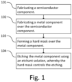
- Fig. 1 is a flowchart outlining the method
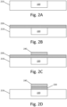
- Figs. 2A to 2D are schematic cross sections of work pieces obtained at various stages of the method.
- the present method may be useful for the fabrication of devices comprising semiconductor-superconductor heterostructures, for example, qubit devices.
- the method may also be applied to other types of devices comprising a combination of semiconductor and metal components.
- a semiconductor component is fabricated.
- the semiconductor component comprises a material of Formula 1: InAs x Sb 1-x where x is in the range 0 to 1.
- An example of a workpiece obtained at this stage is illustrated in Fig. 2A .
- the present method is particularly applicable to indium antimonide. It has been found that indium antimonide is especially susceptible to damage by acidic etchants. Materials according to Formula 1, where x is less than or equal to 0.5, optionally less than or equal to 0.3, optionally less than or equal to 0.25, further optionally less than or equal to 0.1 may be expected to behave similarly to indium antimonide. Materials of Formula 1 where x is less than or equal to 0.3 are expected to behave very similarly to indium antimonide.
- the semiconductor component may be fabricated on substrate.
- the substrate may be any structure on which the device is to be constructed.
- the substrate typically comprises a wafer, i.e. a piece of single crystalline material.
- One example wafer material is indium phosphide.
- Other examples of wafer materials include gallium arsenide, indium antimonide, indium arsenide, and silicon.
- the substrate may be a more elaborate workpiece, further comprising additional structures arranged on or over the wafer.
- the substrate may include layers of two or more materials.
- the substrate may have a planar surface, and the semiconductor component may be grown epitaxially on the planar surface.
- the surface of the substrate may include a channel or trench, and the semiconductor component may be grown in the channel or trench.
- Fig. 2a shows a wafer 210 and a semiconductor component 220 arranged in a channel in the surface of the wafer 210.
- fabricating the semiconductor component in a channel may allow a workpiece having a substantially planar surface to be obtained. This may make the use of lift-off processes at later stages easier.
- the semiconductor component may comprise a nanowire.
- the semiconductor component may take the form of a network of nanowires.
- a network of nanowires comprises two or more interconnected nanowires.
- An SEM image of an example network of nanowires is shown in Fig. 3 .
- the nanowires of the network may be grown simultaneously in a single step.
- the network may be assembled by transferring nanowires from a growth substrate and then subsequently connecting the nanowires together.
- the process used to fabricate the semiconductor component is not particularly limited.
- SAG selective area growth
- SAG comprises forming a mask over the substrate, then growing the semiconductor using e.g. molecular beam epitaxy.
- the mask controls the position at which the semiconductor grows.
- SAG may be particularly useful for constructing networks of nanowires, since the nanowires and junctions between the nanowires can be conveniently formed at the same time by configuring the openings in the mask appropriately.
- VLS vapour-liquid-solid
- VLS forms vertically orientated nanowires on a growth substrate.
- vertically orientated is meant the length direction of the nanowires is perpendicular to the surface of the growth substrate.
- the nanowires may be cleaved from the substrate and then positioned that substrate, or transferred to another substrate as desired.
- the VLS nanowires may remain on the growth substrate, and may be used as components of a vertically-orientated device, such as described in US 2020/0027030 A1 or US 2020/0027971 A1 .
- a network of nanowires may be fabricated by connecting together two or more of VLS grown nanowires.
- a metal component 230 is fabricated over the semiconductor component. This may yield a workpiece as illustrated in Fig. 2B .
- the metal component 230 is typically in the form of a layer.
- the metal component 230 may be arranged on, e.g., may cover, the surface of the substrate 210 and the semiconductor component 220.
- the metal component may have a thickness in the range 2 to 20 nm, optionally 4 to 10 nm.
- the process used to form the metal component 230 is not particularly limited. Examples of useful processes include evaporation and molecular beam epitaxy.
- the metal may be deposited globally, i.e. may cover the surface of the workpiece. Alternatively, the metal may be deposited selectively on selected portions of the surface, for example by using one or more shadow walls to control a directional deposition.
- the metal may be any metal which is compatible with the etchant solution discussed below.
- the metal is alkali-etchable metal.
- Etchants for various metals are disclosed in Walker and Tarn (Eds), "Handbook of Metal Etchants", CRC Press, 1991 .
- the metal may be a superconductor material.
- the metal may be selected from aluminium, lead, vanadium, and tin.
- the metal may be aluminium.
- a hard mask 240 is formed over the metal component 230.
- the hard mask 240 covers regions of the metal component 230 where the metal will be present in the finished device, while exposing regions of the metal component 230 which are to be removed.
- An example workpiece obtained at this stage is shown in Fig. 2C .
- the hard mask may comprise any hard mask material which will not react with the etchant solution described below, and which will adhere to the metal.
- Examples of useful hard mask materials include hafnium oxide, silicon oxide and silicon nitride.
- the hard mask material may be silicon oxide or silicon nitride.
- the hard mask may be patterned using any suitable process, for example by lift-off.
- Lift-off comprises applying a layer of resist over the metal component 230, and then patterning the resist by lithography, typically electron beam lithography. A layer of the hard mask material is then deposited, for example by sputtering. Subsequently, the resist is stripped to yield the hard mask.
- lithography typically electron beam lithography.
- a layer of the hard mask material is then deposited, for example by sputtering. Subsequently, the resist is stripped to yield the hard mask.
- the layer of hard mask material may have any appropriate thickness, for example a thickness in the range 15 to 25 nm, optionally about 20 nm.
- the resist may comprise poly(methyl methacrylate), PMMA.
- PMMA is one illustrative example of an electron beam resist.
- the resist may have a thickness in the range 200 nm to 500 nm.
- An example developer for PMMA comprises a mixture of methyl isobutyl ketone (“MIBK”) and isopropyl alcohol (“IPA”).
- MIBK methyl isobutyl ketone
- IPA isopropyl alcohol
- the ratio of MIBK to IPA may be 1 : 3 by volume.
- Acetone may be used to strip the resist.
- the metal component 230 is etched using an etchant solution.
- the hard mask 240 controls the etch, such that the exposed reasons of the metal component 230 are selectively removed.
- the etchant solution is a basic etchant solution. It has surprisingly been found that the use of a basic etchant solution may allow metal such as aluminium to be etched in the presence of semiconductor materials of Formula 1, without excess damage to the semiconductor material. Using a basic etchant in combination with a hard mask may further allow for high-resolution etching to be achieved. It has been found that the etchant creeps under the mask only to a small extent, and that the shape of the edge of the metal component corresponds well to the shape of the edge of the mask.
- the etchant solution may comprise, as an active component, a strong base.
- strong bases include alkali metal hydroxides such as sodium hydroxide and potassium hydroxide; alkaline earth metal hydroxides such as barium hydroxide; and quaternary ammonium hydroxides such as tetramethyl ammonium hydroxide.
- the etchant solution may comprise tetramethyl ammonium hydroxide as an active component.
- Tetramethyl ammonium hydroxide was investigated in the examples reported below.
- the etchant solution is typically an aqueous solution.
- the solvent may be water, or a cosolvent mixture including water and one or more further solvents, such as a C1 to C5 alkanol. In other implementations, any other suitable polar, protic solvent may be used. Any solvent which allows the active component to behave as a strong base, i.e. to ionise fully, may be used.
- the concentration of the basic etchant is not particularly limited and may be selected as appropriate.
- the concentration may be in the range 0.2 to 3 M.
- the reaction time for the etch may be selected as appropriate depending, for example, the concentration of the etchant, the thickness of the metal component to be etched. Typical reaction times are in the range 40 seconds to 5 minutes. In implementations where the metal is aluminium, the aluminium may remain in contact with the etchant until the silvery colour of the aluminium visibly fades plus about 30 seconds, before terminating the etch.
- the etching may be performed at a temperature of up to 25°C, optionally 20 ⁇ 2 °C. By performing the etch at or below room temperature, diffusion of the metal into the semiconductor material and/or damage to the semiconductor by the etchant may be reduced.
- the etchant solution is typically agitated during the etch.
- the agitation may comprise manual agitation or the use of a magnetic stirrer or the like.
- the etching may be terminated by rinsing.
- Rinsing removes residual etchant from the surface of the chip, thereby improving resolution since any residual etchant may continue to etch the metal film and exacerbate creeping under the mask.
- solvents useful for rinsing are water and isopropanol. Rapid rinsing may allow for improved resolution, for example, the workpiece or chip may be rinsed in a first rinsing bath for about 5 seconds. Multiple sequential rinsing steps may be performed. For example, the workpiece may be rinsed in three sequential rinsing baths. The solvent in each rinsing bath may be independently selected.
- etching After the etching, further operations may be performed as necessary depending on the nature of the desired device. For example, electrical contacts and/or a protective layer of a dielectric may be added.
- a workpiece of the type shown in Fig. 2B was fabricated on an indium phosphide substrate.
- the semiconductor material was InSb, and the metal was aluminium.
- a poly(methylmethacrylate), PMMA, mask was formed over the aluminium.
- PMMA is an example of a soft polymer mask.
- Transene-D is a commercially available acidic etchant which comprises an aqueous solution of phosphoric acid, sodium m -nitrobenzene sulfonate and acetic acid.
- the etch was performed at a temperature of 48.1 °C.
- the reaction time was 14 seconds.
- FIG. 4 An SEM micrograph of the product is shown in Fig. 4 .
- the SEM image shows that the InSb nanowires were etched away, leaving voids. Further, the edges of the etched region have badly defined, rough edges indicative of uncontrolled creeping of the etchant under the mask.
- Transene-D has been reported to give good yields and resolution in indium arsenide / aluminium systems.
- the present results demonstrate that indium antimonide is much more susceptible to damage by acids than indium arsenide.
- Buffered hydrogen fluoride is another commercially available acidic etchant for aluminium. This etchant gave very poor resolution, with a high rate of creep under the mask.
- a workpiece was prepared as described above with reference to Comparative Example 1.
- a PMMA mask was formed over the workpiece.
- the workpiece was then edged using MF321.
- MF321 is a commercially available basic etchant solution, which contains 1.91 % tetramethyl ammonium hydroxide by weight as an active ingredient.
- the reaction time for the etch was 150 seconds.
- An SEM micrograph of the resulting product is shown in Fig. 5 .
- MF321 did not remove the InSb nanowire.
- uncontrolled creeping of the etchant under the mask was observed.
- the extent of the creep was of the order of a few microns.
- the edges of the aluminium were uneven and poorly defined.
- An aluminium layer was fabricated on a substrate, and a PMMA mask was applied.
- the aluminium layer was then etched using aqueous solution comprising 25 % tetramethyl ammonium hydroxide by weight.
- the reaction time for the etch was 20 seconds.
- FIGs. 6a and 6b Micrographs of the product at different levels of magnification are shown in Figs. 6a and 6b .
- the location of one of the etchant windows defined by the mask is shown by dashed lines.
- a workpiece of the type shown in Fig. 2b was fabricated.
- the semiconductor component comprised InSb, and the metal component comprised aluminium.
- a PMMA electron beam resist having a thickness in the range 200 to 500 nm was applied to the workpiece, exposed, and developed using a mixture of MIBK and IPA at a ratio of 1 :3 by volume to form a patterned layer of resist.
- a layer of silicon nitride was then deposited on the workpiece by sputtering, before being formed into a hard mask by lift-off.
- the aluminium was etched using an aqueous solution of tetramethyl ammonium hydroxide, TMAH.
- TMAH tetramethyl ammonium hydroxide
- the reaction time was 3 minutes.
- the product was then inspected using SEM and TEM.
- Fig. 7 is an annotated SEM micrograph of the product.
- the Fig. shows a network of InSb nanowires 720, confirming that the InSb was not removed by the etchant.
- the dark region 740 corresponds to the silicon nitride hard mask. As is typical for sputtered thin films, the hard mask has a rolled edge 742.
- the creeping distance corresponding to the distance from the visible edge of the aluminium under the mask to the edge of the mask, is shown by the white arrow.
- the creeping distance was only about 100 nm, demonstrating an improvement in resolution compared to Comparative Examples 2 and 3.
- the shape of the edge of the aluminium conformed well to the shape of the edge of the mask, showing that the etch was well-controlled.
- Fig. 8 shows a transmission electron microscopy micrograph of the product, taken through a cross-section of one of the nanowires. Slight degradation to the exposed surface of the InSb nanowire, in the region highlighted by ellipse 850, was observed. The damage did not extend beyond a depth of about 5 nm. This is an acceptable degree of damage, and is comparable to the level of damage caused when etching aluminium on InAs using Transene-D.
- the creeping distance corresponding to the distance from the visible edge of the aluminium under the mask to the edge of the mask, is shown by the white arrow.
- the creeping distance was only about 100 nm, demonstrating an improvement in resolution compared to Comparative Examples 2 and 3.
- the shape of the edge of the aluminium conformed well to the shape of the edge of the mask, showing that the etch was well-controlled.
- Fig. 8 shows a transmission electron microscopy micrograph of the product, taken through a cross-section of one of the nanowires. Slight degradation to the exposed surface of the InSb nanowire, in the region highlighted by ellipse 850, was observed. The damage did not extend beyond a depth of about 5 nm. This is an acceptable degree of damage, and is comparable to the level of damage caused when etching aluminium on InAs using Transene-D.
Landscapes
- Engineering & Computer Science (AREA)
- Manufacturing & Machinery (AREA)
- Weting (AREA)
Claims (15)
- Procédé de gravure sélective d'un composant métallique (230) d'une pièce, ce procédé comprenant :la formation (103) d'un masque dur (240) sur le composant métallique (230) ; etla gravure (104) du composant métallique (230) à l'aide d'une solution de gravure, moyennant quoi le masque dur (240) régule la gravure ;dans lequel la solution de gravure est une solution basique de gravure ; etdans lequel la pièce comporte un composant semiconducteur (220) au-dessous du composant métallique (230) comprenant un matériau de formule 1 :
InAsxSb1-x
où x est compris entre 0 et 1. - Procédé selon la revendication 1, dans lequel le composant métallique (230) comprend un métal choisi parmi l'aluminium, le plomb, le vanadium et l'étain.
- Procédé selon la revendication 2, dans lequel le métal est de l'aluminium.
- Procédé selon l'une quelconque des revendications précédentes, où x est compris entre 0 et 0,25, dans lequel éventuellement le composant semiconducteur comprend de l'antimoniure d'indium.
- Procédé selon l'une quelconque des revendications précédentes, dans lequel la solution basique de gravure comporte une base forte, dans lequel éventuellement la base forte est choisie parmi l'hydroxyde de sodium, l'hydroxyde de potassium et l'hydroxyde de tétraméthyl-ammonium.
- Procédé selon la revendication 5, dans lequel la base forte est l'hydroxyde de tétraméthyl-ammonium.
- Procédé selon l'une quelconque des revendications précédentes, dans lequel le masque dur (240) comprend un matériau choisi parmi l'oxyde de silicium, le nitrure de silicium et un oxyde de hafnium.
- Procédé selon la revendication 7, dans lequel le masque dur (240) comprend un nitrure de silicium.
- Procédé selon l'une quelconque des revendications précédentes, dans lequel le masque dur (240) est formé par pulvérisation et par retrait.
- Procédé selon l'une quelconque des revendications précédentes, dans lequel le composant métallique (230) est à la surface du composant semiconducteur (220).
- Procédé selon l'une quelconque des revendications précédentes, dans lequel le composant semiconducteur (220) comprend un nanofil, dans lequel éventuellement le composant semiconducteur (220) comprend un réseau de nanofils.
- Procédé selon l'une quelconque des revendications précédentes, dans lequel la pièce comprend en outre une tranche (210) de matériau cristallin et dans lequel le composant semiconducteur (220) est sur une surface de la tranche (210) ou dans un canal à la surface de la tranche (210).
- Procédé selon la revendication 12, dans lequel le matériau cristallin est le phosphure d'indium.
- Procédé selon la revendication 12 ou la revendication 13, le procédé comprenant en outre, avant la formation du masque dur (240) :la fabrication (101) du composant semiconducteur (220) ; etla fabrication (102) par la suite du composant métallique (230) sur le composant semiconducteur (220) et la surface de la tranche (210).
- Procédé selon la revendication 14, dans lequel le composant semiconducteur (220) est fabriqué à l'aide d'une croissance sélective de surface et/ou dans lequel le composant métallique (230) est fabriqué par épitaxie à faisceau moléculaire.
Applications Claiming Priority (1)
| Application Number | Priority Date | Filing Date | Title |
|---|---|---|---|
| PCT/EP2020/087828 WO2022135726A1 (fr) | 2020-12-23 | 2020-12-23 | Procédé de gravure sélective d'un composant métallique |
Publications (2)
| Publication Number | Publication Date |
|---|---|
| EP4268290A1 EP4268290A1 (fr) | 2023-11-01 |
| EP4268290B1 true EP4268290B1 (fr) | 2025-04-30 |
Family
ID=74130234
Family Applications (1)
| Application Number | Title | Priority Date | Filing Date |
|---|---|---|---|
| EP20838103.8A Active EP4268290B1 (fr) | 2020-12-23 | 2020-12-23 | Procédé de gravure sélective d'un composant métallique |
Country Status (3)
| Country | Link |
|---|---|
| US (1) | US20230420268A1 (fr) |
| EP (1) | EP4268290B1 (fr) |
| WO (1) | WO2022135726A1 (fr) |
Citations (1)
| Publication number | Priority date | Publication date | Assignee | Title |
|---|---|---|---|---|
| WO2021110275A1 (fr) * | 2019-12-05 | 2021-06-10 | Microsoft Technology Licensing Llc | Procédé de gravure sélective d'un composant métallique |
Family Cites Families (5)
| Publication number | Priority date | Publication date | Assignee | Title |
|---|---|---|---|---|
| US8951808B2 (en) * | 2009-02-27 | 2015-02-10 | D-Wave Systems Inc. | Systems and methods for fabrication of superconducting integrated circuits |
| GB201718897D0 (en) | 2017-11-15 | 2017-12-27 | Microsoft Technology Licensing Llc | Superconductor-semiconductor fabrication |
| US10665701B2 (en) | 2018-07-20 | 2020-05-26 | Microsoft Technology Licensing, Llc | Form and fabrication of semiconductor-superconductor nanowires and quantum devices based thereon |
| CN114072915B (zh) * | 2019-02-15 | 2025-05-02 | 微软技术许可有限责任公司 | 使用倾斜沉积和阴影壁的制造方法 |
| US11107965B2 (en) * | 2019-11-11 | 2021-08-31 | International Business Machines Corporation | Majorana fermion quantum computing devices fabricated with ion implant methods |
-
2020
- 2020-12-23 WO PCT/EP2020/087828 patent/WO2022135726A1/fr not_active Ceased
- 2020-12-23 US US18/252,032 patent/US20230420268A1/en active Pending
- 2020-12-23 EP EP20838103.8A patent/EP4268290B1/fr active Active
Patent Citations (1)
| Publication number | Priority date | Publication date | Assignee | Title |
|---|---|---|---|---|
| WO2021110275A1 (fr) * | 2019-12-05 | 2021-06-10 | Microsoft Technology Licensing Llc | Procédé de gravure sélective d'un composant métallique |
Also Published As
| Publication number | Publication date |
|---|---|
| US20230420268A1 (en) | 2023-12-28 |
| EP4268290A1 (fr) | 2023-11-01 |
| WO2022135726A1 (fr) | 2022-06-30 |
Similar Documents
| Publication | Publication Date | Title |
|---|---|---|
| EP4354358B1 (fr) | Fabrication d'un dispositif hybride semi-conducteur-supraconducteur | |
| EP3695440B1 (fr) | Procédés de fabrication | |
| EP4070390B1 (fr) | Procédé de gravure sélective d'un composant métallique | |
| US12525461B2 (en) | Hard mask liftoff processes | |
| US20230420268A1 (en) | Method for selectively etching a metal component | |
| US12581869B2 (en) | Side-gated semiconductor-superconductor hybrid devices | |
| US20230354720A1 (en) | Method of patterning a layer of superconductor material | |
| WO2024039396A1 (fr) | Procédé de fabrication d'un dispositif à semi-conducteur par dépôt à masque | |
| US20230227996A1 (en) | Method of forming shadow walls for fabricating patterned structures | |
| US20240373762A1 (en) | Semiconductor-superconductor hybrid device having a tunnel barrier |
Legal Events
| Date | Code | Title | Description |
|---|---|---|---|
| STAA | Information on the status of an ep patent application or granted ep patent |
Free format text: STATUS: UNKNOWN |
|
| STAA | Information on the status of an ep patent application or granted ep patent |
Free format text: STATUS: THE INTERNATIONAL PUBLICATION HAS BEEN MADE |
|
| PUAI | Public reference made under article 153(3) epc to a published international application that has entered the european phase |
Free format text: ORIGINAL CODE: 0009012 |
|
| STAA | Information on the status of an ep patent application or granted ep patent |
Free format text: STATUS: REQUEST FOR EXAMINATION WAS MADE |
|
| 17P | Request for examination filed |
Effective date: 20230613 |
|
| AK | Designated contracting states |
Kind code of ref document: A1 Designated state(s): AL AT BE BG CH CY CZ DE DK EE ES FI FR GB GR HR HU IE IS IT LI LT LU LV MC MK MT NL NO PL PT RO RS SE SI SK SM TR |
|
| DAV | Request for validation of the european patent (deleted) | ||
| DAX | Request for extension of the european patent (deleted) | ||
| STAA | Information on the status of an ep patent application or granted ep patent |
Free format text: STATUS: EXAMINATION IS IN PROGRESS |
|
| 17Q | First examination report despatched |
Effective date: 20240724 |
|
| REG | Reference to a national code |
Ref country code: DE Ref legal event code: R079 Free format text: PREVIOUS MAIN CLASS: H01L0039240000 Ipc: H10N0060010000 Ref country code: DE Ref legal event code: R079 Ref document number: 602020050553 Country of ref document: DE Free format text: PREVIOUS MAIN CLASS: H01L0039240000 Ipc: H10N0060010000 |
|
| RIC1 | Information provided on ipc code assigned before grant |
Ipc: G06N 10/40 20220101ALI20241126BHEP Ipc: H10N 60/01 20230101AFI20241126BHEP |
|
| GRAP | Despatch of communication of intention to grant a patent |
Free format text: ORIGINAL CODE: EPIDOSNIGR1 |
|
| STAA | Information on the status of an ep patent application or granted ep patent |
Free format text: STATUS: GRANT OF PATENT IS INTENDED |
|
| INTG | Intention to grant announced |
Effective date: 20250117 |
|
| GRAS | Grant fee paid |
Free format text: ORIGINAL CODE: EPIDOSNIGR3 |
|
| GRAA | (expected) grant |
Free format text: ORIGINAL CODE: 0009210 |
|
| STAA | Information on the status of an ep patent application or granted ep patent |
Free format text: STATUS: THE PATENT HAS BEEN GRANTED |
|
| P01 | Opt-out of the competence of the unified patent court (upc) registered |
Free format text: CASE NUMBER: APP_8647/2025 Effective date: 20250220 |
|
| AK | Designated contracting states |
Kind code of ref document: B1 Designated state(s): AL AT BE BG CH CY CZ DE DK EE ES FI FR GB GR HR HU IE IS IT LI LT LU LV MC MK MT NL NO PL PT RO RS SE SI SK SM TR |
|
| REG | Reference to a national code |
Ref country code: CH Ref legal event code: EP Ref country code: GB Ref legal event code: FG4D |
|
| REG | Reference to a national code |
Ref country code: DE Ref legal event code: R096 Ref document number: 602020050553 Country of ref document: DE |
|
| REG | Reference to a national code |
Ref country code: IE Ref legal event code: FG4D |
|
| REG | Reference to a national code |
Ref country code: NL Ref legal event code: MP Effective date: 20250430 |
|
| REG | Reference to a national code |
Ref country code: AT Ref legal event code: MK05 Ref document number: 1791353 Country of ref document: AT Kind code of ref document: T Effective date: 20250430 |
|
| PG25 | Lapsed in a contracting state [announced via postgrant information from national office to epo] |
Ref country code: FI Free format text: LAPSE BECAUSE OF FAILURE TO SUBMIT A TRANSLATION OF THE DESCRIPTION OR TO PAY THE FEE WITHIN THE PRESCRIBED TIME-LIMIT Effective date: 20250430 Ref country code: ES Free format text: LAPSE BECAUSE OF FAILURE TO SUBMIT A TRANSLATION OF THE DESCRIPTION OR TO PAY THE FEE WITHIN THE PRESCRIBED TIME-LIMIT Effective date: 20250430 Ref country code: PT Free format text: LAPSE BECAUSE OF FAILURE TO SUBMIT A TRANSLATION OF THE DESCRIPTION OR TO PAY THE FEE WITHIN THE PRESCRIBED TIME-LIMIT Effective date: 20250901 |
|
| REG | Reference to a national code |
Ref country code: LT Ref legal event code: MG9D |
|
| PG25 | Lapsed in a contracting state [announced via postgrant information from national office to epo] |
Ref country code: NO Free format text: LAPSE BECAUSE OF FAILURE TO SUBMIT A TRANSLATION OF THE DESCRIPTION OR TO PAY THE FEE WITHIN THE PRESCRIBED TIME-LIMIT Effective date: 20250730 Ref country code: GR Free format text: LAPSE BECAUSE OF FAILURE TO SUBMIT A TRANSLATION OF THE DESCRIPTION OR TO PAY THE FEE WITHIN THE PRESCRIBED TIME-LIMIT Effective date: 20250731 |
|
| PG25 | Lapsed in a contracting state [announced via postgrant information from national office to epo] |
Ref country code: NL Free format text: LAPSE BECAUSE OF FAILURE TO SUBMIT A TRANSLATION OF THE DESCRIPTION OR TO PAY THE FEE WITHIN THE PRESCRIBED TIME-LIMIT Effective date: 20250430 Ref country code: PL Free format text: LAPSE BECAUSE OF FAILURE TO SUBMIT A TRANSLATION OF THE DESCRIPTION OR TO PAY THE FEE WITHIN THE PRESCRIBED TIME-LIMIT Effective date: 20250430 |
|
| PG25 | Lapsed in a contracting state [announced via postgrant information from national office to epo] |
Ref country code: BG Free format text: LAPSE BECAUSE OF FAILURE TO SUBMIT A TRANSLATION OF THE DESCRIPTION OR TO PAY THE FEE WITHIN THE PRESCRIBED TIME-LIMIT Effective date: 20250430 |
|
| PG25 | Lapsed in a contracting state [announced via postgrant information from national office to epo] |
Ref country code: HR Free format text: LAPSE BECAUSE OF FAILURE TO SUBMIT A TRANSLATION OF THE DESCRIPTION OR TO PAY THE FEE WITHIN THE PRESCRIBED TIME-LIMIT Effective date: 20250430 |
|
| PG25 | Lapsed in a contracting state [announced via postgrant information from national office to epo] |
Ref country code: AT Free format text: LAPSE BECAUSE OF FAILURE TO SUBMIT A TRANSLATION OF THE DESCRIPTION OR TO PAY THE FEE WITHIN THE PRESCRIBED TIME-LIMIT Effective date: 20250430 |
|
| PG25 | Lapsed in a contracting state [announced via postgrant information from national office to epo] |
Ref country code: RS Free format text: LAPSE BECAUSE OF FAILURE TO SUBMIT A TRANSLATION OF THE DESCRIPTION OR TO PAY THE FEE WITHIN THE PRESCRIBED TIME-LIMIT Effective date: 20250731 |
|
| PG25 | Lapsed in a contracting state [announced via postgrant information from national office to epo] |
Ref country code: IS Free format text: LAPSE BECAUSE OF FAILURE TO SUBMIT A TRANSLATION OF THE DESCRIPTION OR TO PAY THE FEE WITHIN THE PRESCRIBED TIME-LIMIT Effective date: 20250830 |
|
| PG25 | Lapsed in a contracting state [announced via postgrant information from national office to epo] |
Ref country code: LV Free format text: LAPSE BECAUSE OF FAILURE TO SUBMIT A TRANSLATION OF THE DESCRIPTION OR TO PAY THE FEE WITHIN THE PRESCRIBED TIME-LIMIT Effective date: 20250430 |
|
| PGFP | Annual fee paid to national office [announced via postgrant information from national office to epo] |
Ref country code: DE Payment date: 20251126 Year of fee payment: 6 |
|
| PGFP | Annual fee paid to national office [announced via postgrant information from national office to epo] |
Ref country code: GB Payment date: 20251119 Year of fee payment: 6 |
|
| PG25 | Lapsed in a contracting state [announced via postgrant information from national office to epo] |
Ref country code: SM Free format text: LAPSE BECAUSE OF FAILURE TO SUBMIT A TRANSLATION OF THE DESCRIPTION OR TO PAY THE FEE WITHIN THE PRESCRIBED TIME-LIMIT Effective date: 20250430 Ref country code: DK Free format text: LAPSE BECAUSE OF FAILURE TO SUBMIT A TRANSLATION OF THE DESCRIPTION OR TO PAY THE FEE WITHIN THE PRESCRIBED TIME-LIMIT Effective date: 20250430 |
|
| PG25 | Lapsed in a contracting state [announced via postgrant information from national office to epo] |
Ref country code: CZ Free format text: LAPSE BECAUSE OF FAILURE TO SUBMIT A TRANSLATION OF THE DESCRIPTION OR TO PAY THE FEE WITHIN THE PRESCRIBED TIME-LIMIT Effective date: 20250430 |
|
| PG25 | Lapsed in a contracting state [announced via postgrant information from national office to epo] |
Ref country code: EE Free format text: LAPSE BECAUSE OF FAILURE TO SUBMIT A TRANSLATION OF THE DESCRIPTION OR TO PAY THE FEE WITHIN THE PRESCRIBED TIME-LIMIT Effective date: 20250430 |
|
| PG25 | Lapsed in a contracting state [announced via postgrant information from national office to epo] |
Ref country code: SK Free format text: LAPSE BECAUSE OF FAILURE TO SUBMIT A TRANSLATION OF THE DESCRIPTION OR TO PAY THE FEE WITHIN THE PRESCRIBED TIME-LIMIT Effective date: 20250430 |
|
| PG25 | Lapsed in a contracting state [announced via postgrant information from national office to epo] |
Ref country code: IT Free format text: LAPSE BECAUSE OF FAILURE TO SUBMIT A TRANSLATION OF THE DESCRIPTION OR TO PAY THE FEE WITHIN THE PRESCRIBED TIME-LIMIT Effective date: 20250430 |
|
| REG | Reference to a national code |
Ref country code: DE Ref legal event code: R097 Ref document number: 602020050553 Country of ref document: DE |
|
| PG25 | Lapsed in a contracting state [announced via postgrant information from national office to epo] |
Ref country code: RO Free format text: LAPSE BECAUSE OF FAILURE TO SUBMIT A TRANSLATION OF THE DESCRIPTION OR TO PAY THE FEE WITHIN THE PRESCRIBED TIME-LIMIT Effective date: 20250430 |
|
| PLBE | No opposition filed within time limit |
Free format text: ORIGINAL CODE: 0009261 |
|
| STAA | Information on the status of an ep patent application or granted ep patent |
Free format text: STATUS: NO OPPOSITION FILED WITHIN TIME LIMIT |
|
| REG | Reference to a national code |
Ref country code: CH Ref legal event code: L10 Free format text: ST27 STATUS EVENT CODE: U-0-0-L10-L00 (AS PROVIDED BY THE NATIONAL OFFICE) Effective date: 20260311 |
|
| 26N | No opposition filed |
Effective date: 20260202 |