EP4269940A2 - Vorrichtung und verfahren zur inspektion - Google Patents
Vorrichtung und verfahren zur inspektion Download PDFInfo
- Publication number
- EP4269940A2 EP4269940A2 EP23197893.3A EP23197893A EP4269940A2 EP 4269940 A2 EP4269940 A2 EP 4269940A2 EP 23197893 A EP23197893 A EP 23197893A EP 4269940 A2 EP4269940 A2 EP 4269940A2
- Authority
- EP
- European Patent Office
- Prior art keywords
- outline
- images
- relationship information
- virtual plane
- image
- Prior art date
- Legal status (The legal status is an assumption and is not a legal conclusion. Google has not performed a legal analysis and makes no representation as to the accuracy of the status listed.)
- Granted
Links
Images



Classifications
-
- H—ELECTRICITY
- H10—SEMICONDUCTOR DEVICES; ELECTRIC SOLID-STATE DEVICES NOT OTHERWISE PROVIDED FOR
- H10P—GENERIC PROCESSES OR APPARATUS FOR THE MANUFACTURE OR TREATMENT OF DEVICES COVERED BY CLASS H10
- H10P72/00—Handling or holding of wafers, substrates or devices during manufacture or treatment thereof
- H10P72/06—Apparatus for monitoring, sorting, marking, testing or measuring
-
- G—PHYSICS
- G01—MEASURING; TESTING
- G01B—MEASURING LENGTH, THICKNESS OR SIMILAR LINEAR DIMENSIONS; MEASURING ANGLES; MEASURING AREAS; MEASURING IRREGULARITIES OF SURFACES OR CONTOURS
- G01B11/00—Measuring arrangements characterised by the use of optical techniques
- G01B11/24—Measuring arrangements characterised by the use of optical techniques for measuring contours or curvatures
- G01B11/25—Measuring arrangements characterised by the use of optical techniques for measuring contours or curvatures by projecting a pattern, e.g. one or more lines, moiré fringes on the object
- G01B11/2545—Measuring arrangements characterised by the use of optical techniques for measuring contours or curvatures by projecting a pattern, e.g. one or more lines, moiré fringes on the object with one projection direction and several detection directions, e.g. stereo
-
- H—ELECTRICITY
- H10—SEMICONDUCTOR DEVICES; ELECTRIC SOLID-STATE DEVICES NOT OTHERWISE PROVIDED FOR
- H10P—GENERIC PROCESSES OR APPARATUS FOR THE MANUFACTURE OR TREATMENT OF DEVICES COVERED BY CLASS H10
- H10P74/00—Testing or measuring during manufacture or treatment of wafers, substrates or devices
- H10P74/20—Testing or measuring during manufacture or treatment of wafers, substrates or devices characterised by the properties tested or measured, e.g. structural or electrical properties
- H10P74/203—Structural properties, e.g. testing or measuring thicknesses, line widths, warpage, bond strengths or physical defects
-
- G—PHYSICS
- G01—MEASURING; TESTING
- G01B—MEASURING LENGTH, THICKNESS OR SIMILAR LINEAR DIMENSIONS; MEASURING ANGLES; MEASURING AREAS; MEASURING IRREGULARITIES OF SURFACES OR CONTOURS
- G01B11/00—Measuring arrangements characterised by the use of optical techniques
- G01B11/02—Measuring arrangements characterised by the use of optical techniques for measuring length, width or thickness
- G01B11/06—Measuring arrangements characterised by the use of optical techniques for measuring length, width or thickness for measuring thickness ; e.g. of sheet material
-
- G—PHYSICS
- G01—MEASURING; TESTING
- G01B—MEASURING LENGTH, THICKNESS OR SIMILAR LINEAR DIMENSIONS; MEASURING ANGLES; MEASURING AREAS; MEASURING IRREGULARITIES OF SURFACES OR CONTOURS
- G01B11/00—Measuring arrangements characterised by the use of optical techniques
- G01B11/02—Measuring arrangements characterised by the use of optical techniques for measuring length, width or thickness
- G01B11/06—Measuring arrangements characterised by the use of optical techniques for measuring length, width or thickness for measuring thickness ; e.g. of sheet material
- G01B11/0608—Height gauges
-
- G—PHYSICS
- G01—MEASURING; TESTING
- G01B—MEASURING LENGTH, THICKNESS OR SIMILAR LINEAR DIMENSIONS; MEASURING ANGLES; MEASURING AREAS; MEASURING IRREGULARITIES OF SURFACES OR CONTOURS
- G01B11/00—Measuring arrangements characterised by the use of optical techniques
- G01B11/02—Measuring arrangements characterised by the use of optical techniques for measuring length, width or thickness
- G01B11/06—Measuring arrangements characterised by the use of optical techniques for measuring length, width or thickness for measuring thickness ; e.g. of sheet material
- G01B11/0616—Measuring arrangements characterised by the use of optical techniques for measuring length, width or thickness for measuring thickness ; e.g. of sheet material of coating
- G01B11/0625—Measuring arrangements characterised by the use of optical techniques for measuring length, width or thickness for measuring thickness ; e.g. of sheet material of coating with measurement of absorption or reflection
-
- G—PHYSICS
- G01—MEASURING; TESTING
- G01B—MEASURING LENGTH, THICKNESS OR SIMILAR LINEAR DIMENSIONS; MEASURING ANGLES; MEASURING AREAS; MEASURING IRREGULARITIES OF SURFACES OR CONTOURS
- G01B11/00—Measuring arrangements characterised by the use of optical techniques
- G01B11/24—Measuring arrangements characterised by the use of optical techniques for measuring contours or curvatures
- G01B11/25—Measuring arrangements characterised by the use of optical techniques for measuring contours or curvatures by projecting a pattern, e.g. one or more lines, moiré fringes on the object
- G01B11/2518—Projection by scanning of the object
- G01B11/2527—Projection by scanning of the object with phase change by in-plane movement of the patern
-
- G—PHYSICS
- G01—MEASURING; TESTING
- G01B—MEASURING LENGTH, THICKNESS OR SIMILAR LINEAR DIMENSIONS; MEASURING ANGLES; MEASURING AREAS; MEASURING IRREGULARITIES OF SURFACES OR CONTOURS
- G01B11/00—Measuring arrangements characterised by the use of optical techniques
- G01B11/24—Measuring arrangements characterised by the use of optical techniques for measuring contours or curvatures
- G01B11/25—Measuring arrangements characterised by the use of optical techniques for measuring contours or curvatures by projecting a pattern, e.g. one or more lines, moiré fringes on the object
- G01B11/254—Projection of a pattern, viewing through a pattern, e.g. moiré
-
- G—PHYSICS
- G01—MEASURING; TESTING
- G01B—MEASURING LENGTH, THICKNESS OR SIMILAR LINEAR DIMENSIONS; MEASURING ANGLES; MEASURING AREAS; MEASURING IRREGULARITIES OF SURFACES OR CONTOURS
- G01B11/00—Measuring arrangements characterised by the use of optical techniques
- G01B11/26—Measuring arrangements characterised by the use of optical techniques for measuring angles or tapers; for testing the alignment of axes
-
- H—ELECTRICITY
- H10—SEMICONDUCTOR DEVICES; ELECTRIC SOLID-STATE DEVICES NOT OTHERWISE PROVIDED FOR
- H10P—GENERIC PROCESSES OR APPARATUS FOR THE MANUFACTURE OR TREATMENT OF DEVICES COVERED BY CLASS H10
- H10P74/00—Testing or measuring during manufacture or treatment of wafers, substrates or devices
- H10P74/23—Testing or measuring during manufacture or treatment of wafers, substrates or devices characterised by multiple measurements, corrections, marking or sorting processes
-
- H—ELECTRICITY
- H10—SEMICONDUCTOR DEVICES; ELECTRIC SOLID-STATE DEVICES NOT OTHERWISE PROVIDED FOR
- H10P—GENERIC PROCESSES OR APPARATUS FOR THE MANUFACTURE OR TREATMENT OF DEVICES COVERED BY CLASS H10
- H10P74/00—Testing or measuring during manufacture or treatment of wafers, substrates or devices
- H10P74/23—Testing or measuring during manufacture or treatment of wafers, substrates or devices characterised by multiple measurements, corrections, marking or sorting processes
- H10P74/235—Testing or measuring during manufacture or treatment of wafers, substrates or devices characterised by multiple measurements, corrections, marking or sorting processes comprising optical enhancement of defects or not-directly-visible states
-
- H—ELECTRICITY
- H10—SEMICONDUCTOR DEVICES; ELECTRIC SOLID-STATE DEVICES NOT OTHERWISE PROVIDED FOR
- H10P—GENERIC PROCESSES OR APPARATUS FOR THE MANUFACTURE OR TREATMENT OF DEVICES COVERED BY CLASS H10
- H10P74/00—Testing or measuring during manufacture or treatment of wafers, substrates or devices
- H10P74/27—Structural arrangements therefor
-
- G—PHYSICS
- G01—MEASURING; TESTING
- G01B—MEASURING LENGTH, THICKNESS OR SIMILAR LINEAR DIMENSIONS; MEASURING ANGLES; MEASURING AREAS; MEASURING IRREGULARITIES OF SURFACES OR CONTOURS
- G01B11/00—Measuring arrangements characterised by the use of optical techniques
- G01B11/24—Measuring arrangements characterised by the use of optical techniques for measuring contours or curvatures
- G01B11/25—Measuring arrangements characterised by the use of optical techniques for measuring contours or curvatures by projecting a pattern, e.g. one or more lines, moiré fringes on the object
- G01B11/2513—Measuring arrangements characterised by the use of optical techniques for measuring contours or curvatures by projecting a pattern, e.g. one or more lines, moiré fringes on the object with several lines being projected in more than one direction, e.g. grids, patterns
-
- G—PHYSICS
- G01—MEASURING; TESTING
- G01B—MEASURING LENGTH, THICKNESS OR SIMILAR LINEAR DIMENSIONS; MEASURING ANGLES; MEASURING AREAS; MEASURING IRREGULARITIES OF SURFACES OR CONTOURS
- G01B11/00—Measuring arrangements characterised by the use of optical techniques
- G01B11/24—Measuring arrangements characterised by the use of optical techniques for measuring contours or curvatures
- G01B11/25—Measuring arrangements characterised by the use of optical techniques for measuring contours or curvatures by projecting a pattern, e.g. one or more lines, moiré fringes on the object
- G01B11/2518—Projection by scanning of the object
-
- G—PHYSICS
- G01—MEASURING; TESTING
- G01B—MEASURING LENGTH, THICKNESS OR SIMILAR LINEAR DIMENSIONS; MEASURING ANGLES; MEASURING AREAS; MEASURING IRREGULARITIES OF SURFACES OR CONTOURS
- G01B2210/00—Aspects not specifically covered by any group under G01B, e.g. of wheel alignment, caliper-like sensors
- G01B2210/56—Measuring geometric parameters of semiconductor structures, e.g. profile, critical dimensions or trench depth
Definitions
- the present disclosure relates to a technology for inspection.
- various inspections are conducted to check if various treatments, processes and the like for a semiconductor have been properly performed. For example, an inspection may be conducted as to whether a device such as a die or the like to be installed on a semiconductor substrate is positioned at a correct position on the semiconductor substrate.
- a die may be mounted on solder or solder balls while the solder or solder balls are applied to the substrate.
- the die needs to be mounted so that the lower surface of the die is parallel to the reference plane of the semiconductor substrate.
- the die may be mounted in a state in which it is tilted at a certain angle or more with respect to the semiconductor substrate due to certain factors (e.g., the applied state of the solder or solder balls). Since this is a factor that may cause defects in a semiconductor device, whether the die is tilted and if tilted, at what angle or more the die is tilted should be able to be confirmed in the inspection process of the semiconductor.
- a three-dimensional inspection machine that irradiates three-dimensional illumination light on a semiconductor die may be used.
- this method has a problem in that it is difficult to acquire a three-dimensional shape for a die to be inspected. This is because, in general, the upper surface of the semiconductor die is made of a reflector, so that the irradiated three-dimensional illumination light may be totally reflected on the upper surface of the semiconductor die and, consequently, the image of the semiconductor die may not be captured well.
- a device utilizing a White Light Scanning Interferometry may be used in order to conduct the above-described tilt inspection.
- this method has a problem in that, when a semiconductor die is tilted at a certain angle (e.g., 1.2 degrees) or more with respect to a reference plane, an image of the die is not formed.
- a two-dimensional area inspection may be used in order to conduct the above-described tilt inspection.
- the semiconductor die looks like a parallelogram depending on the degree of tilt.
- the two-dimensional area inspection is a method that derives a degree of tilt through the shape of the parallelogram.
- this method also has a problem in that, when the upper surface of the semiconductor die is made of a reflector, an accurate parallelogram shape cannot be acquired, and the degree of tilt of the semiconductor die cannot be accurately predicted.
- the present disclosure provides a technique for inspection to solve the above-mentioned problems of the related art.
- an apparatus for inspection can be proposed.
- the apparatus may include: at least one first light source configured to irradiate illumination light to an object on a reference plane; one or more cameras configured to capture one or more illumination images generated by the illumination light reflected from the object; and one or more processors configured to: determine one or more outlines indicating edges of the object on the one or more illumination images; determine height values of an edge of an upper surface of the object with respect to the reference plane based on the one or more outlines; and determine a first angle between the upper surface of the object and the reference plane based on the height values.
- the apparatus may further include: at least one second light source configured to irradiate pattern light to the object, wherein the one or more cameras may be further configured to capture one or more pattern images generated by the pattern light reflected from the object, and the one or more processors are further configured to determine the one or more outlines indicating the edges of the object based on the one or more illumination images and the one or more pattern images, determine a virtual plane corresponding to the upper surface of the object based on the one or more outlines, and determine a second angle between the virtual plane and the reference plane as the first angle.
- the one or more cameras may include a top camera configured to capture an illumination image or a pattern image from above the object, and one or more side cameras configured to capture illumination images or pattern images from one or more sides of the object.
- At least one among the one or more illumination images and the one or more pattern images may be a top image captured from above the object by the top camera, and the other images among the one or more illumination images and the one or more pattern images may be side images captured from one or more sides of the object by the one or more side cameras.
- the one or more processors may be further configured to extract a first outline from the top image and a second outline from the one or more side images, the first and second outlines indicating the same one edge of the object, and determine the virtual plane based on the first outline and the second outline.
- the one or more processors may be further configured to determine first relationship information indicating a correspondence relationship between the first outline and the second outline, and determine the virtual plane based on the first relationship information.
- a first point on the first outline may correspond to a second point on the second outline
- the first relationship information may include a pair of coordinate information of the first point on the top image and coordinate information of the second point on the one or more side images.
- the one or more processors may be further configured to extract a third outline from one side image and a fourth outline from another side image among the one or more side images, the third and fourth outlines indicating the same one edge of the object, determine second relationship information indicating a correspondence relationship between the third outline and the fourth outline, and determine the virtual plane based on the first relationship information and the second relationship information.
- the one or more processors may be further configured to determine the virtual plane by selecting images in which contrast values of a surface of the object are equal to or greater than a predetermined value, from among the one or more illumination images and the one or more pattern images.
- the object may have a form in which a plurality of layers are stacked, and the one or more outlines may indicate edges of the plurality of layers.
- the one or more processors may be further configured to determine a plurality of virtual planes corresponding to the plurality of layers based on the one or more outlines, and determine a spacing between the plurality of layers based on the plurality of virtual planes corresponding to the plurality of layers.
- a method for inspection may be proposed.
- the method according to another aspect of the present disclosure may include: irradiating, by at least one first light source, illumination light to an object on a reference plane; capturing, by one or more cameras, one or more illumination images generated by the illumination light reflected from the object; determining, by one or more processors, one or more outlines indicating edges of the object on the one or more illumination images; determining, by the one or more processors, height values of an edge of an upper surface of the object with respect to the reference plane based on the one or more outlines; and determining, by the one or more processors, a first angle between the upper surface of the object and the reference plane based on the height values.
- the method may further include: irradiating, by at least one second light source, pattern light to the object; capturing, by the one or more cameras, one or more pattern images generated by the pattern light reflected from the object; determining, by the one or more processors, the one or more outlines indicating the edges of the object based on the one or more illumination images and the one or more pattern images; determining, by the one or more processors, a virtual plane corresponding to the upper surface of the object based on the one or more outlines; and determining, by the one or more processors, a second angle between the virtual plane and the reference plane as the first angle.
- the one or more cameras may include a top camera configured to capture an illumination image or a pattern image from above the object, and one or more side cameras configured to capture illumination images or pattern images from one or more sides of the object.
- At least one among the one or more illumination images and the one or more pattern images may be a top image captured from above the object by the top camera, and the other images among the one or more illumination images and the one or more pattern images may be side images captured from one or more sides of the object by the one or more side cameras.
- the determining the virtual plane may include extracting a first outline from the top image and a second outline from the one or more side images, the first and second outlines indicating the same one edge of the object, and determining the virtual plane based on the first outline and the second outline.
- the determining the virtual plane may include determining first relationship information indicating a correspondence relationship between the first outline and the second outline, and determining the virtual plane based on the first relationship information.
- a first point on the first outline may correspond to a second point on the second outline
- the first relationship information may include a pair of coordinate information of the first point on the top image and coordinate information of the second point on the one or more side images.
- the determining the virtual plane may include extracting a third outline from one side image and a fourth outline from another side image among the one or more side images, the third and fourth outlines indicating the same one edge of the object, determining second relationship information indicating a correspondence relationship between the third outline and the fourth outline, and determining the virtual plane based on the first relationship information and the second relationship information.
- the determining the virtual plane may include determining the virtual plane by selecting images in which contrast values of a surface of the object are equal to or greater than a predetermined value, from among the one or more illumination images and the one or more pattern images.
- a non-transitory computer-readable recording medium that stores a program to be executed on a computer.
- the program includes commands that, when executed by one or more processors, cause the one or more processors to perform: determining one or more outlines indicating edges of an object on one or more illumination images generated by illumination light irradiated to the object on a reference plane and reflected from the object; determining height values of an edge of an upper surface of the object with respect to the reference plane based on the one or more outlines; and determining a first angle between the upper surface of the object and the reference plane based on the height values.
- an accurate virtual three-dimensional model for an object may be generated by acquiring an image using light irradiated from various types of light sources at various angles and in various directions.
- the expressions such as “include”, “may include”, “provided with”, “may be provided with”, “have”, and “may have” mean the presence of subject features (e.g., functions, operations, components, etc.) and do not exclude the presence of other additional features. That is, such expressions should be understood as open-ended terms that imply the possibility of including other embodiments.
- first used herein are used to identify a plurality of components from one another, and are not intended to limit the order or importance of the relevant components.
- the expressions such as “A, B and C”, “A, B or C”, “A, B and/or C”, “at least one of A, B and C", “ at least one of A, B or C", “at least one of A, B and/or C", “at least one selected from A, B and C", “at least one selected from A, B or C", and “at least one selected from A, B and/or C” may mean each of the listed items or all available combinations of the listed items.
- the expression “at least one selected from A and B” may refer to (1) at least one A, (2) at least one B, and (3) both at least one A and at least one B.
- the expression "based on” used herein is used to describe one or more factors that influences a decision, an action of judgment or an operation described in a phrase or sentence including the relevant expression, and this expression does not exclude additional factor influencing the decision, the action of judgment or the operation.
- a certain component e.g., a first component
- another component e.g., a second component
- the expression that a certain component is "connected" to another component may mean that the certain component is connected to another component either directly or via a new different component (e.g., a third component).
- a processor configured to perform a specific operation may mean a generic-purpose processor capable of performing a specific operation by executing software.
- an object may refer to an object positioned on a predetermined surface and inspected by an apparatus.
- the object may be a die, a semiconductor device or a chip positioned on a semiconductor substrate.
- the object may be mounted on a semiconductor substrate.
- the object may be mounted such that the lower surface of the object is tilted at a predetermined angle with respect to a reference plane of a substrate.
- the substrate may be a surface on which an object is positioned.
- the substrate may be a semiconductor substrate.
- the reference plane of the substrate may refer to a surface of a substrate, and may be a surface used as a reference for measuring a tilt angle with a lower surface of an object.
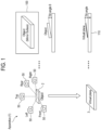
- FIG. 1 is a diagram illustrating a process of operation of an apparatus according to an embodiment of the present disclosure.
- the apparatus 1 may measure an angle ⁇ at which an object 2 is tilted with respect to a reference plane (e.g., a substrate, etc.).
- the object 2 e.g., a die, etc.
- the object 2 may be arranged on the reference plane.
- the object 2 may be disposed in a state 100 in which it is tilted at a predetermined angle ⁇ with respect to the reference plane.
- the apparatus 1 according to an embodiment of the present disclosure may inspect whether or not installation of the object 2 is defective, by measuring (determining) the tilt angle.
- illumination light sources of the apparatus 1 may irradiate two-dimensional illumination light onto the object 2 located on the reference plane.
- the illumination light may be reflected from surfaces of the object 2, i.e., the top surface or one or more side surfaces.
- One or more cameras 50 of the apparatus 1 may capture one or more illumination images generated by the reflection of the illumination light from the object 2.
- the apparatus 1 may determine one or more outlines indicating edges of the object 2 on the acquired one or more illumination images.
- Each of the illuminated images may be a two-dimensional photograph representing the object 2 and/or the edges of the object 2.
- the edges of the object may mean the respective sides of the shape of the object existing in an actual three-dimensional space (e.g., the respective sides of a cube).
- the outlines may mean the edges of the object appearing on the image of the object (i.e., the lines appearing on the image). In the present disclosure, the outlines may be referred to as boundary lines.
- the apparatus 1 may determine a height value of each point of the edge of the upper surface of the object 2 with respect to the reference plane, based on the determined one or more outlines. Furthermore, the apparatus 1 may determine a tilt angle ⁇ between the upper surface of the object 2 and the reference plane based on the corresponding height values.
- the height value of the edge of the upper surface of the object may indicate a distance at which the each point of the corresponding edge is spaced apart from the reference plane. Accordingly, when the height values of the edge of the upper surface of the object are determined, it is possible to know the angle of the corresponding edge with respect to the reference plane. Accordingly, it is possible to determine at what angle the upper surface of the object is tilted with respect to the reference plane.
- the apparatus 1 may determine the tilt angle of the object by additionally using pattern light in addition to the illumination light.
- the pattern light source of the apparatus 1 may irradiate pattern light toward the object 2.
- the pattern light may be reflected from the surfaces of the object 2, i.e., the upper surface or one or more side surfaces of the object 2.
- the one or more cameras 50 of the apparatus 1 may capture one or more pattern images generated by the pattern light reflected from the object 2.
- the apparatus 1 may determine one or more outlines indicating the edges of the object 2 based on one or more illumination images and/or one or more pattern images.
- the apparatus 1 may determine a virtual plane 3 corresponding to the upper surface of the object 2 based on the determined one or more outlines 110.
- the virtual plane 3 may be a plane on which the upper surface of the object 2 in an actual three-dimensional space is virtually implemented using computer graphics.
- the apparatus 1 may determine an angle between the virtual plane 3 and the reference plane as an angle ⁇ between the object 2 and the reference plane 110.
- the object 2 may be a stacked memory in which a plurality of layers are stacked.
- one or more extracted outlines may indicate edges of the plurality of layers of the object 2.
- the apparatus 1 may determine a plurality of virtual planes based on one or more outlines acquired from an image of the object 2 having a stacked structure. The process of determining the virtual planes is as described above. Each of the determined virtual planes may correspond to each of the plurality of layers of the object 2 having the stacked structure. That is, one virtual plane may represent one of a plurality of layers.
- the apparatus 1 may determine a gap between the layers of the object 2 having the stacked structure, based on each of the determined virtual planes. In one embodiment, this process may be performed by the processor of the apparatus 1.
- the apparatus 1 can measure a tilt angle of the object 2 by using the virtual plane of the object 2. In addition, according to various embodiments of the present disclosure, even when the object is tilted at a specific angle (e.g., 1.2 degrees) or more with respect to the reference plane, the apparatus 1 can generate a virtual plane to determine the degree of tilt of the object 2.
- a specific angle e.g., 1.2 degrees
- the apparatus 1 can generate a virtual plane to determine the degree of tilt of the object 2.
- FIG. 2 is a block diagram of the apparatus according to an embodiment of the present disclosure.
- the apparatus 1 may include one or more processors 10, one or more memories 20, one or more pattern light sources 30, one or more illumination light sources 40 and/or one or more cameras 50.
- at least one of these components of the apparatus 1 may be omitted, or another component may be added to the apparatus 1.
- some components may be integrated, or may be implemented as a singular entity or plural entities.
- one or more components e.g., one or more processors
- a component e.g., processor 10
- At least some of the internal and external components of the apparatus 1 may be connected to each other via a bus, a general purpose input/output (GPIO), a serial peripheral interface (SPI), a mobile industry processor interface (MIPI) and the like to exchange data and/or signals.
- GPIO general purpose input/output
- SPI serial peripheral interface
- MIPI mobile industry processor interface
- the illumination light sources 40 may irradiate two-dimensional illumination light onto the object 2.
- the illumination light may be RGB light
- each of the illumination light sources 40 may include a red light source that irradiates red light, a green light source that irradiates green light, and a blue light source that irradiates blue light.
- the respective illumination light sources 40 may saturate the surface of the object by irradiating all of the red light, the green light and the blue light.
- the pattern light sources 30 may irradiate pattern light onto the object 2.
- the pattern light may be any structured light, grid pattern light (light whose luminous intensity changes in a sine wave pattern), line light, and the like.
- the pattern light sources 30 may irradiate pattern light that is phase-shifted by a grating transfer mechanism such as a piezo actuator (PZT), or may irradiate pattern light generated by a digital light processing (DLP) method or a liquid crystal on silicon (LCoS) method.
- each of the one or more pattern light sources 30 may irradiate the pattern light according to a method selected from the method using PZT, the DLP method and the LCoS method.
- one or more (e.g., eight) pattern light sources 30 that irradiate pattern light in different directions from above the object 2 may be used.
- the cameras 50 may capture illumination images and/or pattern images as described above.
- the cameras 50 may be implemented as charge coupled devices (CCDs) or complementary metal oxide semiconductor (CMOS) cameras.
- the one or more cameras 50 may include a top camera and/or one or more side cameras.
- the top camera may capture an illumination image or a pattern image reflected from the object 2 on the upper side of the object 2.
- Each of the one or more side cameras may capture an illumination image or a pattern image reflected from the object 2 on the lateral side or the upper lateral side of the object 2.
- the one or more side cameras may include four cameras corresponding to the front, rear, left and right sides of the object 2.
- an illumination image or a pattern image captured by the top camera on the upper side of the object 2 may be referred to as a top image.
- illumination images or pattern images captured by one or more side cameras on one or more lateral sides of the object 2 may be referred to as side images. That is, some among the above-described one or more illumination images and one or more pattern images may be top images, and other images among those may be side images.
- the processor 10 may control at least one component of the apparatus 1 connected to the processor 10 by driving software (e.g., instructions, programs, etc.). In addition, the processor 10 may perform various operations related to the present disclosure, such as calculation, treatment, data generation, processing and the like. Further, the processor 10 may load data or the like from the memory 20 or may store data in the memory 20. In one embodiment, the processor 10 may determine one or more outlines of the object 2 on the one or more illumination images, may determine height values of an edge of the upper surface of the object 2 based on the one or more outlines, and may determine an angle ⁇ between the upper surface of the object and the reference plane based on the height values.
- driving software e.g., instructions, programs, etc.
- the processor 10 may perform various operations related to the present disclosure, such as calculation, treatment, data generation, processing and the like.
- the processor 10 may load data or the like from the memory 20 or may store data in the memory 20.
- the processor 10 may determine one or more outlines of the object 2 on the one or more
- the processor 10 may determine one or more outlines indicating the edges of the object 2 based on the one or more illumination images and/or the one or more pattern images, may determine a virtual plane 3 corresponding to the upper surface of the object based on the one or more outlines, and may determine an angle between the virtual plane 3 and the reference plane as an angle ⁇ at which the object 2 is tilted.
- the memory 20 may store various types of data.
- the data stored in the memory 20 is data acquired, processed or used by at least one component of the apparatus 1, and may include software (e.g., instructions, programs, etc.).
- the memory 20 may include a volatile memory and/or a nonvolatile memory.
- the instructions or programs are software stored in the memory 20, and may include an operating system for controlling the resources of the apparatus 1, an application, and/or middleware that provides various functions to the application so that the application can utilize the resources of the apparatus 1.
- the memory 20 may store commands that, when executed by the processor 10, cause the processor 10 to perform an operation.
- the apparatus 1 may further include a transceiver (not shown).
- the transceiver may perform wireless or wired communication between the apparatus 1 and a server, or between the apparatus 1 and other devices.
- the transceiver 230 may perform wireless communication according to a method such as eMBB (enhanced Mobile Broadband), URLLC (Ultra Reliable Low-Latency Communication), MMTC (Massive Machine Type Communication), LTE (Long-Term Evolution), LTE-A (LTE Advance), NR (New Radio), UMTS (Universal Mobile Telecommunications System), GSM (Global System for Mobile Communication), CDMA (Code Division Multiple Access), WCDMA (Wideband CDMA), WiBro (Wireless Broadband), WiFi (Wireless Fidelity), Bluetooth, NFC (Near Field Communication), GPS (Global Positioning System), or GNSS (Global Navigation Satellite System).
- eMBB enhanced Mobile Broadband
- URLLC Ultra Reliable Low-Latency Communication
- MMTC Massive Machine Type Communication
- LTE Long-
- the transceiver may perform wired communication according to a method such as USB (Universal Serial Bus), HDMI (High Definition Multimedia Interface), RS-232 (Recommended Standard-232), or POTS (Plain Old Telephone Service).
- the processor 10 may acquire information from the server by controlling the transceiver.
- the information acquired from the server may be stored in the memory 20.
- the information acquired from the server may include parameters or various kinds of information which are necessary to extract outlines from an image, determine relationship information between the extracted outlines, or generate a virtual three-dimensional model 3.
- the information acquired from the server may include an intrinsic or extrinsic parameter value of the camera 50 for calibration of the camera 50.
- the apparatus 1 may further include a user interface (not shown).
- the user interface may receive an input from a user and may output (display) information to the user.
- the user interface may include an input device and/or an output device.
- the input device may be a device that receives information, which is to be transmitted to at least one component of the apparatus 1, from the outside.
- the input device may include a mouse, a keyboard, a touch pad and the like.
- the output device may be a device that provides various kinds of information on the apparatus 1 to a user in a visual form.
- the output device may include a display, a projector, a hologram, and the like.
- the user interface may receive parameters that can be used for inspection of the object 2 from the user, or may display the determined tilt angle ⁇ of the object 2 to the user.
- the apparatus 1 may be an apparatus of various types.
- the apparatus 1 may be a portable communication apparatus, a computer apparatus, a portable multimedia apparatus, or a combination of two or more of the aforementioned apparatuses.
- the apparatus 1 of the present disclosure is not limited to the aforementioned apparatuses.
- FIG. 1 Various embodiments of the apparatus 1 according to the present disclosure may be combined with each other. The respective embodiments may be combined according to the number of cases, and the embodiments of the apparatus 1 made by such combination also fall within the scope of the present disclosure.
- the internal/external components of the apparatus 1 according to the present disclosure described above may be added, modified, replaced or deleted depending on the embodiments.
- the internal/external components of the apparatus 1 described above may be implemented as hardware components.
- FIG. 3 is a diagram illustrating a process of generating a virtual plane with respect to an upper surface of an object according to an embodiment of the present disclosure.
- the process of generating the virtual plane 3 may include a calibration process, an outline extraction process, a determination process of relationship information between the outlines, and/or a generation process of a virtual plane.
- the apparatus 1 may calibrate the cameras 50.
- the apparatus 1 may acquire basic information necessary to generate a virtual plane for the upper surface of the object.
- the apparatus 1 may acquire position information (i.e., origin position information) of each of the cameras 50.
- the origin position of each of the cameras 50 may mean a position of a point in a three-dimensional space when each of the cameras is viewed as a point.
- the position of each of the cameras 50 may appear as a position relative to the object 2 or may appear as an absolute position in a three-dimensional space coordinate system.
- the apparatus 1 may acquire view angle information and/or intrinsic parameters of each of the cameras 50.
- the information acquired during the calibration process may be stored in the memory 20.
- the calibration-related information may be acquired from the server through the transceiver.
- the calibration process is an optional process and may be omitted.
- the processor 10 may extract outlines from the top image and the side image. Among the extracted outlines, there may be outlines that indicate the same one edge of the object 2 on different images. For example, the processor 10 may extract an outline (hereinafter referred to as first outline) indicating one edge of the object 2 from the top image, and may extract an outline (hereinafter referred to as second outline) indicating the same corresponding edge from the side image.
- first outline an outline indicating one edge of the object 2 from the top image
- second outline an outline
- the processor 10 may determine (derive) relationship information (hereinafter referred to as first relationship information) between the first outline and the second outline.
- first relationship information relationship information
- the edge of the object 2 indicated by the two outlines may be an edge shared by two adjacent surfaces of the object 2.
- one point (hereinafter referred to as first point) on the first outline and one point (hereinafter referred to as second point) on the second outline may commonly represent one point (hereinafter referred to as target point) on the actual edge of the object and, therefore, may correspond to each other.
- target point When looking at the target point from the top camera, the target point may be represented as the first point on the top image.
- the straight line may appear as a two-dimensional straight line on the corresponding side image.
- This two-dimensional straight line is called an epipolar line for the first point.
- An intersection point between the epipolar line for the first point and the second outline may be derived from the corresponding side image.
- This intersection point may be the aforementioned second point (i.e., a point corresponding to the first point).
- the transformation from the first point to the epipolar line for the first point may be defined by a fundamental matrix, which is a concept according to the epipolar geometry.
- the fundamental matrix may be derived from the camera calibration information described above.
- the first relationship information may include information on two corresponding points (the first point and the second point).
- the first relationship information may be a pair of two-dimensional pixel coordinates of these two points (the first point and the second point), a pair of three-dimensional space coordinates of these two points, or a transformation relation or transformation matrix between the two-dimensional pixel coordinates or between the three-dimensional space coordinates.
- the processor 10 may determine (generate) a virtual plane 3 corresponding to the upper surface of the object by using the determined first relationship information. Specifically, the processor 10 may acquire a vector from the origin of the top camera to the coordinates of the first point and a vector from the origin of the side camera to the coordinates of the second point using the first relationship information, and may derive a point where the two vectors meet. Using the points derived in this manner, three-dimensional modeling may be performed on the entire upper surface of the obj ect.
- the generation process of the virtual plane 3 has been described above based on the top image and one side (left) image.
- the virtual plane 3 may be generated by using two different side images among the plurality of side images.
- the processor 10 may extract an outline (hereinafter referred to as third outline) indicating one edge of the object 2 from one of the side images, and may extract an outline (hereinafter referred to as fourth outline) indicating the same corresponding edge from another side image.
- the processor 10 may further acquire relationship information (hereinafter referred to as second relationship information) indicating a correspondence relationship between the third and fourth outlines.
- the processor 10 may determine the virtual plane 3 based on the first relationship information and/or the second relationship information.
- the determination process (acquiring process) of relationship information from the images by the processor 10 may be repeated a plurality of times.
- the determination process of the relationship information may be repeated a plurality of times according to combinations of a top image and side images.
- the processor 10 may perform the determination process of relationship information a plurality of times, by changing the images used to determine (acquire) relationship information on the same surface depending on the types of the illumination images or the pattern images.
- the processor 10 may perform the determination process of relationship information on the same surface a plurality of times, depending on the irradiation angles and directions of the illumination light sources or the pattern light sources.
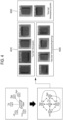
- FIG. 4 is a diagram explaining acquisition of various images and combination of the images for determining relationship information according to an embodiment of the present disclosure.
- the apparatus 1 may acquire a plurality of images from an object.
- the acquired images may vary depending on the type of the light used, the irradiation direction of the light used, the irradiation angle of the light used, and the like.
- the apparatus 1 may acquire a plurality of illumination images or pattern images in one direction of the object, depending on whether the light used for image capture is illumination light or pattern light. That is, for the same surface of the object, a plurality of images may be acquired according to the type of the light used.
- the apparatus 1 may acquire a plurality of images in one direction of the object depending on the direction or angle in which the pattern light source 30 or the illumination light source 40 irradiates light onto the object.
- one or more pattern light sources 30 may be disposed at various positions (e.g., 8-way positions) to irradiate pattern light toward the object. The arrangement of the pattern light sources 30 will be described later.
- a plurality of pattern images may be acquired for the same surface of the object.
- one or more illumination light sources 40 may irradiate illumination light toward the object at various angles. The arrangement of the illumination light sources 40 will be described later.
- a plurality of illumination images may be acquired for the same surface of the object.
- the apparatus 1 may select images for different directions (the top image, the side image in each direction, etc.) from the illumination images or the pattern images acquired for the respective directions of the object as described above, and may determine relationship information between the outlines from the two images.
- the processor 10 may select the top image and one side image, and may determine first relationship information from the selected images.
- the top image may represent the upper surface of the object
- the one side image may represent the upper surface and one or more side surfaces of the object. Since the upper and side surfaces of the object share edges, the first relationship information may be determined from the top image and the side image. For example, when the object has a rectangular parallelepiped shape, four pieces of first relationship information may be determined.
- the processor 10 may select side images of two different directions from among the one or more side images, and may determine second relationship information from the selected images.
- the two side images may represent two adjacent side surfaces of the object. Since the two adjacent side surfaces share an edge of the object, the second relationship information may be determined from the two side images. For example, when the object has a rectangular parallelepiped shape, four pieces of second relationship information may be determined.
- the processor 10 may select two side images representing two side surfaces of the object, which do not share an edge, from among the one or more side images, and may determine relationship information (hereinafter referred to as third relationship information) from the selected images.
- third relationship information may be determined using an epipolar line.
- two parallel side surfaces may have two parallel edges.
- a point on one outline on one side image may appear as a straight line (epipolar line) on the other parallel side image.
- a point at which the epipolar line intersects an outline in the other side image may correspond to the point in the original side image.
- Third relationship information indicating this correspondence relationship may be determined. For example, when the object has a rectangular parallelepiped shape, two pieces of third relationship information may be determined.
- the processor 10 may determine a virtual plane 3 for the upper surface of the object by using at least one of the above-described first relationship information, second relationship information and/or third relationship information. Various pieces of relationship information can be acquired according to the combination of two images from which the relationship information is determined, the irradiation direction or angle, the type of illumination, and the like. The processor 10 can more accurately generate a virtual plane by utilizing the various pieces of relationship information.
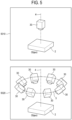
- FIG. 5 is a diagram illustrating a form in which one or more pattern light sources 30 according to an embodiment of the present disclosure are arranged.
- the apparatus 1 may include one or more pattern light sources 30.
- the pattern light sources 30 may be disposed at various positions around the object 2 to irradiate pattern light toward the object 2.
- the pattern light source 30 may be one light source positioned on a normal line 4 of the upper surface of the object 2 and configured to irradiate pattern light toward the object 2.
- the normal line 4 perpendicular to the upper surface of the object 2 may be drawn.
- the one pattern light source 30 may be positioned at a point on the normal line 4.
- the pattern light source 30 may irradiate pattern light toward the upper surface of the object 2.
- the normal line 4 may be drawn as a half line extending from the center of the upper surface of the object 2 toward the opposite side of the reference plane.
- the distance between the one pattern light source 30 and the object 2 may be changed.
- the one pattern light source 30 may sequentially irradiate the pattern light toward the object 2 several times while changing the phase of the pattern of the pattern light.
- the pattern light sources 30 may be a plurality of pattern light sources 30 arranged on a concentric circle 5 above the upper surface of the object. Specifically, it may be possible to assume a concentric circle 5, which has a center on the normal line 4 of the upper surface of the object and is parallel to the reference plane. A plurality of pattern light sources 30 may be disposed on the circumference of the concentric circle 5. The pattern light sources 30 may irradiate pattern light toward the object 2. In some embodiments, the radius of the concentric circle 5 may be changed. In some embodiments, the spacing between the pattern light sources 30 arranged on the concentric circle 5 may be changed.
- the pattern light sources 30 may be disposed on the circumference of the concentric circles 5 at equal intervals, or may be disposed on the circumference of the concentric circles 5 at different intervals which are arbitrarily set. In one embodiment, eight pattern light sources 30 may be arranged at intervals of 45 degrees. The arrangement of the plurality of pattern light sources 30 in this case may be referred to as an 8-way arrangement. In one embodiment, the pattern light sources 30 may sequentially irradiate pattern light toward the object 2. In one embodiment, the patterns of the pattern light irradiated by the pattern light sources 30 may have different phases.
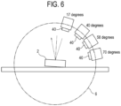
- FIG. 6 is a diagram illustrating a form in which one or more illumination light sources according to an embodiment of the present disclosure are arranged.
- the apparatus 1 may include the one or more illumination light sources 40.
- the illumination light sources 40 may be disposed at various positions around the object to irradiate illumination light toward the object.
- the illumination light sources 40 may be a plurality of illumination light sources 40 arranged on a concentric circle 6 perpendicular to the reference plane. Specifically, it may be possible to assume a concentric circle 6, which has a center at the object and is perpendicular to the reference plane.
- the illumination light sources 40 may be disposed on the circumference of the concentric circle 6.
- the illumination light sources 40 may irradiate illumination light toward the object.
- the radius of the concentric circle 6 may be changed.
- the spacing of the illumination light sources 40 arranged on the concentric circle 6 may be changed.
- the illumination light sources 40 may be arranged on the circumference of the concentric circle 6 at equal intervals, or may be arranged on the circumference of the concentric circle 6 at different intervals which are arbitrarily set.
- each of the illumination light sources 40 may be arranged at an arbitrary angle.
- the angle may mean an angle of the position of each of the illumination light sources 40 on the circumference of the concentric circle 6 with respect to the normal line of the reference plane.
- At least one of the illumination light sources 40 may be disposed at a large angle of 70 degrees or more (a small angle with respect to the reference plane). In one embodiment, the illumination light sources 40 may be arranged at angles of 17 degrees, 40 degrees, 58 degrees and 70 degrees, respectively. In one embodiment, the illumination light sources 40 may be arranged only above the reference plane. In one embodiment, the illumination light sources 40 may sequentially irradiate illumination light toward the object 2. In one embodiment, the illumination light irradiated by the illumination light sources 40 may have different wavelengths. In one embodiment, each of the illumination light sources 40 may include a red light source, a green light source and a blue light source, which are capable of irradiating red light, green light and blue light, respectively.
- the illumination light sources 40 may first irradiate light of one wavelength (e.g., red light) to the object sequentially for each arrangement angle. Thereafter, the illumination light sources 40 may irradiate light of another wavelength (e.g., green light) to the object sequentially for each arrangement angle. Then, the illumination light sources 40 may irradiate light of the remaining wavelength (e.g., blue light) to the object sequentially for each arrangement angle. In one embodiment, the illumination light sources 40 may sequentially irradiate red light, green light and blue light for one angle, and then may sequentially irradiate red light, green light and blue light for the next angle.
- one wavelength e.g., red light
- the illumination light sources 40 may sequentially irradiate light of another wavelength (e.g., green light) to the object sequentially for each arrangement angle.
- the illumination light sources 40 may irradiate light of the remaining wavelength (e.g., blue light) to the object sequentially for each arrangement angle.
- the order of irradiation may be changed according to the intention of a designer.
- the respective illumination light sources 40 may simultaneously irradiate red light, green light and blue light to irradiate mixed white light to the object.
- each of the illumination light sources 40 may irradiate ordinary white light rather than the mixed white light to the object.
- the illumination light sources 40 arranged at different angles may simultaneously irradiate mixed white light to saturate the surface of the object. In this case, the reflected illumination light may be captured to acquire an illumination image of the surface of the object.
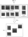
- FIG. 7 is a diagram illustrating an image filtering process according to an embodiment of the present disclosure.
- the processor 10 may filter the images acquired according to various factors (the type of light, the irradiation direction, the angle, etc.) based on predetermined criteria, and then may generate a virtual plane 3 by using only the image selected from the image filtering process.
- the apparatus 1 inspects an object (e.g., a die) on a substrate, the inspection may be affected by other elements and irregularities on the substrate. Due to this effect, distortion may occur in the acquired images, or distortion may occur in the outlines acquired from the images.
- the virtual plane 3 is generated based on a distorted image or a distorted outline, it may be difficult to accurately measure or inspect the object 2. In order to prevent this, only the image filtered based on the predetermined criteria may be selected and used to generate the virtual plane 3.
- the processor 10 may perform the image filtering process based on whether or not a contrast value of the surface of the object 2 appearing on the image is equal to or greater than a predetermined value.
- the processor 10 may discard the images having a contrast value less than the predetermined value, may select only the images having contrast values equal to or greater than the predetermined value, and may determine (derive) the aforementioned relationship information therefrom.
- the processor 10 may perform the image filtering process based on whether or not the outlines appearing on the images have continuity.
- the processor 10 may select only the images in which the outline indicating one edge of the object appears as a line segment having continuity, and may determine the aforementioned relationship information therefrom.
- the processor 10 may statistically calculate an average or median value of the outline position coordinates extracted from a plurality of images, and may exclude the image from which an outline having position coordinates deviating from the average or median value by a predetermined ratio or more is extracted. In this case, the processor 10 may determine the aforementioned relationship information based on only the images that are not excluded.
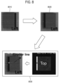
- FIG. 8 is a diagram illustrating a process of deriving another outline from one outline of an image according to an embodiment of the present disclosure.
- the processor 10 may determine another outline from one outline using the pre-stored specification information on the object 2. As described above, when the apparatus 1 inspects the object on the substrate, the inspection may be affected by other elements and irregularities of the substrate. Accordingly, it may not be possible to extract the outline required for determining the relationship information. In this case, in order to supplement the outline extraction process, another outline may be derived from one outline by using the pre-stored specification information on the object 2.
- the memory 20 may include the specification information on the object 2.
- the specification information may include width, length and height information on the object 2.
- the processor 10 may predict and derive a position of an outline parallel to the corresponding outline by using the specification information. For example, it may be assumed that an outline 8010 of the lower surface of the object 2 has been extracted and an outline of the upper surface of the object 2 parallel to the outline of the lower surface has not been extracted due to a predetermined distortion. In this case, the processor 10 may acquire height information on the object 2 based on the specification information, and may apply the height information to the extracted outline of the lower surface to predict the position of the outline of the upper surface parallel to the outline of the lower surface. In this way, it is possible to extract an outline of the upper surface 8020.
- the processor 10 may first extract an outline parallel to the required outline, and then may acquire the required outline by applying the specification information as described above.
- the processor 10 may determine relationship information by using the outline required for determining the relationship information 8030.
- the specification information may include information on the shape of the object.
- the specification information may store information on the radius and height of a cylinder.
- the processor 10 may derive another outline required for determining relationship information from one outline by using the radius and height information.
- the memory 20 may serve as a database for storing specification information of objects to be inspected.
- the memory 20 may store specification information on objects (e.g., devices, chips, etc.) positioned on a substrate or used in general.
- the processor 10 may identify an object from the acquired images, and then may read specification information corresponding to the identified object from the memory 20.
- the processor 10 may derive another outline required for determining relationship information from one outline of the identified object based on the acquired specification information.
- the processor 10 may acquire specification information of objects from a server by controlling a transceiver. The acquired specification information may be stored in the memory 20.
- FIG. 9 is a diagram showing an example of a method for inspection, which may be performed by the apparatus 1 according to the present disclosure.
- the method for inspection according to the present disclosure may be a computer-implemented method.
- the respective steps of the method or algorithm according to the present disclosure have been described in a sequential order in the illustrated flowchart, the respective steps may be performed in an order that can be arbitrarily combined by the present disclosure, in addition to being performed sequentially.
- the description in accordance with this flowchart does not exclude making changes or modifications to the method or algorithm, and does not imply that any step is necessary or desirable.
- at least some of the steps may be performed in parallel, repetitively or heuristically.
- at least some of the steps may be omitted, or other steps may be added.
- the apparatus 1 may perform a method for inspection according to various embodiments of the present disclosure.
- a method according to an embodiment of the present disclosure may include irradiating illumination light to an object on a reference plane (S910), capturing one or more illumination images generated by illumination light reflected from the object (S920), determining one or more outlines indicating edges of the object on the one or more illumination images (S930), determining height values of an edge of an upper surface of the object with respect to the reference plane based on the one or more outlines (S940), and/or determining a first angle between the upper surface of the object and the reference plane based on the height values (S950).
- At least one first light source (e.g., the illumination light source 40) of the apparatus 1 may irradiate illumination light to the object 2 on the reference plane.
- the one or more cameras 50 of the apparatus 1 may capture one or more illumination images generated by the illumination light reflected from the object 2.
- the one or more processors 10 of the apparatus 1 may determine one or more outlines indicating the edges of the object 2 on the one or more illumination images.
- the processors 10 may determine height values of the edge of the upper surface of the object with respect to the reference plane based on the one or more outlines.
- the processors 10 may determine a first angle (e.g., an angle ⁇ ) between the upper surface of the object and the reference plane based on the height values.
- the method according to the present disclosure may further include irradiating, by at least one second light source (e.g., the pattern light source 30) of the apparatus 1, pattern light to the object 2, capturing, by the one or more cameras 50, one or more pattern images generated by the pattern light reflected from the object 2, determining, by the processor 10, one or more outlines indicating the edges of the object 2 based on the one or more illumination images and the one or more pattern images, determining, by the processor 10, a virtual plane 3 corresponding to the upper surface of the object 2 based on the one or more outlines, and/or determining, by the processor 10, a second angle between the virtual plane 3 and the reference plane as the first angle.
- the second light source e.g., the pattern light source 30
- determining the virtual plane may include extracting a first outline from a top image and a second outline from one or more side images.
- the first outline and the second outline may indicate the same one edge of the object 2.
- Determining the virtual plane may further include determining the virtual plane 3 based on the first outline and the second outline.
- determining the virtual plane may further include determining first relationship information indicating a correspondence relationship between the first outline and the second outline, and/or determining the virtual plane 3 based on the first relationship information.
- determining the virtual plane may further include extracting a third outline from one side image and a fourth outline from another side image.
- the third outline and the fourth outline may indicate the same one edge of the object among the one or more side images.
- Determining the virtual plane may further include determining second relationship information indicating a correspondence relationship between the third outline and the fourth outline, and/or determining the virtual plane 3 based on the first relationship information and the second relationship information.
- determining the virtual plane may further include selecting images in which contrast values of a surface of the object are equal to or greater than a predetermined value, from among the one or more illumination images and the one or more pattern images to determine the virtual plane 3.
- the software may be software for implementing the various embodiments of the present disclosure described above.
- the software may be inferred from various embodiments of the present disclosure by programmers in the art to which the present disclosure belongs.
- the software may be commands (e.g., code or code segments) or programs that can be read by a device.
- the device is a device capable of operating according to commands called from a recording medium, and may be, for example, a computer.
- the device may be the electronic apparatus 1 according to embodiments of the present disclosure.
- the processor of the device may execute the called commands so that the components of the device can perform a function corresponding to the commands.
- the processor may be one or more processors 10 according to the embodiments of the present disclosure.
- the recording medium may refer to any type of device-readable recording medium in which data is stored.
- the recording medium may include, for example, a ROM, a RAM, a CD-ROM, a magnetic tape, a floppy disk, an optical data storage device, and the like.
- the recording medium may be one or more memories 20.
- the recording medium may be implemented in such a form that it is distributed in computer systems connected by a network.
- the software may be distributed, stored and executed in a computer system or the like.
- the recording medium may be a non-transitory recording medium.
- the non-transitory recording medium refers to a tangible medium irrespective of whether data is stored semi-permanently or temporarily, and does not include a signal propagating in a transitory manner.
- the present invention discloses the following items:
Landscapes
- Physics & Mathematics (AREA)
- General Physics & Mathematics (AREA)
- Engineering & Computer Science (AREA)
- Computer Vision & Pattern Recognition (AREA)
- Length Measuring Devices By Optical Means (AREA)
- Manufacturing & Machinery (AREA)
- Image Analysis (AREA)
- Investigating Materials By The Use Of Optical Means Adapted For Particular Applications (AREA)
Applications Claiming Priority (3)
| Application Number | Priority Date | Filing Date | Title |
|---|---|---|---|
| KR20180122323 | 2018-10-15 | ||
| PCT/KR2019/013396 WO2020080758A1 (ko) | 2018-10-15 | 2019-10-11 | 검사를 위한 장치, 방법 및 명령을 기록한 기록 매체 |
| EP19873586.2A EP3869542B1 (de) | 2018-10-15 | 2019-10-11 | Vorrichtung und verfahren zur inspektion |
Related Parent Applications (2)
| Application Number | Title | Priority Date | Filing Date |
|---|---|---|---|
| EP19873586.2A Division-Into EP3869542B1 (de) | 2018-10-15 | 2019-10-11 | Vorrichtung und verfahren zur inspektion |
| EP19873586.2A Division EP3869542B1 (de) | 2018-10-15 | 2019-10-11 | Vorrichtung und verfahren zur inspektion |
Publications (4)
| Publication Number | Publication Date |
|---|---|
| EP4269940A2 true EP4269940A2 (de) | 2023-11-01 |
| EP4269940A3 EP4269940A3 (de) | 2023-11-29 |
| EP4269940C0 EP4269940C0 (de) | 2025-07-09 |
| EP4269940B1 EP4269940B1 (de) | 2025-07-09 |
Family
ID=70284709
Family Applications (2)
| Application Number | Title | Priority Date | Filing Date |
|---|---|---|---|
| EP23197893.3A Active EP4269940B1 (de) | 2018-10-15 | 2019-10-11 | Vorrichtung und verfahren zur inspektion |
| EP19873586.2A Active EP3869542B1 (de) | 2018-10-15 | 2019-10-11 | Vorrichtung und verfahren zur inspektion |
Family Applications After (1)
| Application Number | Title | Priority Date | Filing Date |
|---|---|---|---|
| EP19873586.2A Active EP3869542B1 (de) | 2018-10-15 | 2019-10-11 | Vorrichtung und verfahren zur inspektion |
Country Status (5)
| Country | Link |
|---|---|
| US (2) | US11694916B2 (de) |
| EP (2) | EP4269940B1 (de) |
| KR (2) | KR102264682B1 (de) |
| CN (2) | CN112805816B (de) |
| WO (1) | WO2020080758A1 (de) |
Families Citing this family (2)
| Publication number | Priority date | Publication date | Assignee | Title |
|---|---|---|---|---|
| KR102695597B1 (ko) * | 2020-12-14 | 2024-08-19 | 가부시키가이샤 신가와 | 반도체 장치의 제조 장치 및 제조 방법 |
| KR20230053767A (ko) | 2021-10-14 | 2023-04-24 | 삼성디스플레이 주식회사 | 표시 장치용 검사 장치 및 검사 방법 |
Family Cites Families (46)
| Publication number | Priority date | Publication date | Assignee | Title |
|---|---|---|---|---|
| JP3914638B2 (ja) * | 1997-09-09 | 2007-05-16 | シーケーディ株式会社 | 形状計測装置 |
| JPH11166818A (ja) * | 1997-12-04 | 1999-06-22 | Suzuki Motor Corp | 三次元形状計測装置の校正方法及び校正装置 |
| JP2961264B1 (ja) | 1998-09-21 | 1999-10-12 | 工業技術院長 | 3次元物体モデル生成方法及び3次元物体モデル生成プログラムを記録したコンピュータ読み取り可能な記録媒体 |
| DE19963345A1 (de) * | 1999-12-27 | 2001-07-05 | Leica Microsystems | Optische Messanordnung und Verfahren zur Neigungsmessung |
| JP2001308594A (ja) | 2000-04-24 | 2001-11-02 | Sony Corp | 位置調整装置及び方法 |
| JP3609325B2 (ja) | 2000-06-08 | 2005-01-12 | シーケーディ株式会社 | 三次元計測装置 |
| JP3878023B2 (ja) * | 2002-02-01 | 2007-02-07 | シーケーディ株式会社 | 三次元計測装置 |
| US7193728B2 (en) * | 2002-08-07 | 2007-03-20 | Advantest Corporation | Processing apparatus, processing method and position detecting device |
| CH697278B1 (de) * | 2003-09-12 | 2008-07-31 | Oerlikon Assembly Equipment Ag | Einrichtung und Verfahren für die Montage oder Verdrahtung von Halbleiterchips. |
| SG138491A1 (en) * | 2006-06-21 | 2008-01-28 | Generic Power Pte Ltd | Method and apparatus for 3-dimensional vision and inspection of ball and like protrusions of electronic components |
| WO2008068136A1 (de) * | 2006-12-07 | 2008-06-12 | Esec Ag | Verfahren und einrichtung zur messung einer höhendifferenz |
| KR20090062027A (ko) | 2007-12-12 | 2009-06-17 | 삼성전기주식회사 | 3차원자세측정장치 및 이를 이용한 3차원자세측정방법 |
| KR101081538B1 (ko) | 2009-02-25 | 2011-11-08 | 주식회사 고영테크놀러지 | 3차원 형상 측정장치 및 측정방법 |
| CN103134446B (zh) | 2008-02-26 | 2017-03-01 | 株式会社高永科技 | 三维形状测量装置及测量方法 |
| JP2010071782A (ja) | 2008-09-18 | 2010-04-02 | Omron Corp | 3次元計測装置およびその方法 |
| JP2010091338A (ja) * | 2008-10-06 | 2010-04-22 | Nec Electronics Corp | 傾き検査装置および傾き検査方法 |
| KR101237497B1 (ko) * | 2009-03-30 | 2013-02-26 | 주식회사 고영테크놀러지 | 검사영역의 설정방법 |
| JP4715944B2 (ja) | 2009-04-03 | 2011-07-06 | オムロン株式会社 | 三次元形状計測装置、三次元形状計測方法、および三次元形状計測プログラム |
| US9091725B2 (en) * | 2009-07-03 | 2015-07-28 | Koh Young Technology Inc. | Board inspection apparatus and method |
| JP5471356B2 (ja) * | 2009-11-24 | 2014-04-16 | オムロン株式会社 | 3次元計測のためのキャリブレーション方法および3次元視覚センサ |
| KR101164208B1 (ko) * | 2010-04-19 | 2012-07-10 | 주식회사 고영테크놀러지 | 기판 검사장치 |
| JP2012002780A (ja) * | 2010-06-21 | 2012-01-05 | Shinko Electric Ind Co Ltd | 形状計測装置、形状計測方法、および半導体パッケージの製造方法 |
| GB201019537D0 (en) * | 2010-11-18 | 2010-12-29 | 20X20 Vision Ltd | PCB reflow inspection angled measurement |
| JP5912553B2 (ja) * | 2012-01-12 | 2016-04-27 | ヤマハ発動機株式会社 | プリント基板の複合検査装置 |
| TWI475597B (zh) * | 2012-02-08 | 2015-03-01 | 日立全球先端科技股份有限公司 | Pattern evaluation method and pattern evaluation device |
| DE102012207653A1 (de) * | 2012-05-08 | 2013-11-14 | Dr. Johannes Heidenhain Gmbh | Verfahren und Vorrichtung zum Vermessen von Kanten eines Objektes |
| CN103733019B (zh) * | 2012-07-24 | 2017-03-01 | 精益视觉科技私人有限公司 | 用于确定集成电路封装的共面性的方法和装置 |
| JP5843241B2 (ja) | 2013-11-26 | 2016-01-13 | レーザーテック株式会社 | 検査装置、及び検査方法 |
| JP6424020B2 (ja) * | 2014-06-09 | 2018-11-14 | 株式会社キーエンス | 画像検査装置、画像検査方法、画像検査プログラム及びコンピュータで読み取り可能な記録媒体並びに記録した機器 |
| JP6303867B2 (ja) | 2014-06-27 | 2018-04-04 | オムロン株式会社 | 基板検査装置及びその制御方法 |
| JP2016021514A (ja) * | 2014-07-15 | 2016-02-04 | キヤノンマシナリー株式会社 | 半導体チップ姿勢検出装置及び半導体チップ姿勢検出方法 |
| KR102178978B1 (ko) * | 2014-07-31 | 2020-11-13 | 한국전자통신연구원 | 스테레오 매칭 방법 및 이를 수행하는 장치 |
| KR101628158B1 (ko) * | 2014-12-05 | 2016-06-09 | 주식회사 미르기술 | 3차원 형상 측정 장치 |
| US10533952B2 (en) | 2014-12-08 | 2020-01-14 | Koh Young Technology Inc. | Method of inspecting a terminal of a component mounted on a substrate and substrate inspection apparatus |
| US9694498B2 (en) | 2015-03-30 | 2017-07-04 | X Development Llc | Imager for detecting visual light and projected patterns |
| KR101659302B1 (ko) * | 2015-04-10 | 2016-09-23 | 주식회사 고영테크놀러지 | 3차원 형상 측정장치 |
| KR101639227B1 (ko) | 2015-06-08 | 2016-07-13 | 주식회사 고영테크놀러지 | 3차원 형상 측정장치 |
| KR101705762B1 (ko) * | 2015-09-02 | 2017-02-14 | 주식회사 미르기술 | 3차원 형상 측정 장치의 틸트 교정 방법 |
| KR20170036222A (ko) | 2015-09-24 | 2017-04-03 | 세메스 주식회사 | 다이 검사 방법 |
| WO2017181338A1 (en) * | 2016-04-19 | 2017-10-26 | Abb Schweiz Ag | Tilt detection apparatus and method thereof |
| KR101809558B1 (ko) | 2016-05-20 | 2017-12-22 | 이동현 | 3차원 모델 생성 시스템 및 그 방법 |
| JP6691838B2 (ja) * | 2016-06-27 | 2020-05-13 | 株式会社キーエンス | 測定装置 |
| US10458912B2 (en) * | 2016-08-31 | 2019-10-29 | Kla-Tencor Corporation | Model based optical measurements of semiconductor structures with anisotropic dielectric permittivity |
| US10841561B2 (en) * | 2017-03-24 | 2020-11-17 | Test Research, Inc. | Apparatus and method for three-dimensional inspection |
| KR20170124509A (ko) * | 2017-10-31 | 2017-11-10 | 주식회사 고영테크놀러지 | 검사 시스템 및 검사 방법 |
| JP7181292B2 (ja) * | 2018-06-26 | 2022-11-30 | 株式会社Fuji | 平坦度取得システムおよび実装機 |
-
2019
- 2019-10-11 CN CN201980065992.7A patent/CN112805816B/zh active Active
- 2019-10-11 KR KR1020190126390A patent/KR102264682B1/ko active Active
- 2019-10-11 EP EP23197893.3A patent/EP4269940B1/de active Active
- 2019-10-11 US US17/280,037 patent/US11694916B2/en active Active
- 2019-10-11 CN CN202411564010.8A patent/CN119509411A/zh active Pending
- 2019-10-11 EP EP19873586.2A patent/EP3869542B1/de active Active
- 2019-10-11 WO PCT/KR2019/013396 patent/WO2020080758A1/ko not_active Ceased
-
2021
- 2021-06-07 KR KR1020210073420A patent/KR102382769B1/ko active Active
-
2023
- 2023-05-12 US US18/316,413 patent/US12051606B2/en active Active
Also Published As
| Publication number | Publication date |
|---|---|
| WO2020080758A1 (ko) | 2020-04-23 |
| US20230282499A1 (en) | 2023-09-07 |
| EP3869542A4 (de) | 2021-11-24 |
| EP3869542B1 (de) | 2023-12-13 |
| EP3869542A1 (de) | 2021-08-25 |
| KR20210071899A (ko) | 2021-06-16 |
| EP4269940C0 (de) | 2025-07-09 |
| EP4269940B1 (de) | 2025-07-09 |
| KR20200042422A (ko) | 2020-04-23 |
| US11694916B2 (en) | 2023-07-04 |
| US20220037175A1 (en) | 2022-02-03 |
| CN112805816B (zh) | 2024-11-22 |
| KR102264682B1 (ko) | 2021-06-15 |
| US12051606B2 (en) | 2024-07-30 |
| CN112805816A (zh) | 2021-05-14 |
| EP4269940A3 (de) | 2023-11-29 |
| CN119509411A (zh) | 2025-02-25 |
| EP3869542C0 (de) | 2023-12-13 |
| KR102382769B1 (ko) | 2022-04-08 |
Similar Documents
| Publication | Publication Date | Title |
|---|---|---|
| CN108074267B (zh) | 交点检测装置及方法、摄像头校正系统及方法及记录介质 | |
| CN105783784B (zh) | 检查装置及检查装置的控制方法 | |
| EP3992575B1 (de) | Vorrichtung und verfahren zur bestimmung der dreidimensionalen form eines objektes | |
| US12051606B2 (en) | Apparatus, method and recording medium storing command for inspection | |
| JP2017166957A (ja) | 欠陥検出装置、欠陥検出方法およびプログラム | |
| JP6114154B2 (ja) | 欠陥判定装置、欠陥検査装置、および欠陥判定方法 | |
| JP2025030324A (ja) | 検査システム及び検査方法 |
Legal Events
| Date | Code | Title | Description |
|---|---|---|---|
| PUAI | Public reference made under article 153(3) epc to a published international application that has entered the european phase |
Free format text: ORIGINAL CODE: 0009012 |
|
| STAA | Information on the status of an ep patent application or granted ep patent |
Free format text: STATUS: REQUEST FOR EXAMINATION WAS MADE |
|
| REG | Reference to a national code |
Ref country code: DE Ipc: G01B0011260000 Ref country code: DE Ref legal event code: R079 Ref document number: 602019072520 Country of ref document: DE Free format text: PREVIOUS MAIN CLASS: G01B0011250000 Ipc: G01B0011260000 |
|
| PUAL | Search report despatched |
Free format text: ORIGINAL CODE: 0009013 |
|
| 17P | Request for examination filed |
Effective date: 20230918 |
|
| AC | Divisional application: reference to earlier application |
Ref document number: 3869542 Country of ref document: EP Kind code of ref document: P |
|
| AK | Designated contracting states |
Kind code of ref document: A2 Designated state(s): AL AT BE BG CH CY CZ DE DK EE ES FI FR GB GR HR HU IE IS IT LI LT LU LV MC MK MT NL NO PL PT RO RS SE SI SK SM TR |
|
| AK | Designated contracting states |
Kind code of ref document: A3 Designated state(s): AL AT BE BG CH CY CZ DE DK EE ES FI FR GB GR HR HU IE IS IT LI LT LU LV MC MK MT NL NO PL PT RO RS SE SI SK SM TR |
|
| RIC1 | Information provided on ipc code assigned before grant |
Ipc: G01B 11/25 20060101ALI20231025BHEP Ipc: H01L 21/66 20060101ALI20231025BHEP Ipc: G01B 11/26 20060101AFI20231025BHEP |
|
| RBV | Designated contracting states (corrected) |
Designated state(s): AL AT BE BG CH CY CZ DE DK EE ES FI FR GB GR HR HU IE IS IT LI LT LU LV MC MK MT NL NO PL PT RO RS SE SI SK SM TR |
|
| GRAP | Despatch of communication of intention to grant a patent |
Free format text: ORIGINAL CODE: EPIDOSNIGR1 |
|
| STAA | Information on the status of an ep patent application or granted ep patent |
Free format text: STATUS: GRANT OF PATENT IS INTENDED |
|
| INTG | Intention to grant announced |
Effective date: 20250213 |
|
| GRAS | Grant fee paid |
Free format text: ORIGINAL CODE: EPIDOSNIGR3 |
|
| GRAA | (expected) grant |
Free format text: ORIGINAL CODE: 0009210 |
|
| STAA | Information on the status of an ep patent application or granted ep patent |
Free format text: STATUS: THE PATENT HAS BEEN GRANTED |
|
| AC | Divisional application: reference to earlier application |
Ref document number: 3869542 Country of ref document: EP Kind code of ref document: P |
|
| AK | Designated contracting states |
Kind code of ref document: B1 Designated state(s): AL AT BE BG CH CY CZ DE DK EE ES FI FR GB GR HR HU IE IS IT LI LT LU LV MC MK MT NL NO PL PT RO RS SE SI SK SM TR |
|
| REG | Reference to a national code |
Ref country code: GB Ref legal event code: FG4D |
|
| REG | Reference to a national code |
Ref country code: CH Ref legal event code: EP |
|
| REG | Reference to a national code |
Ref country code: IE Ref legal event code: FG4D |
|
| U01 | Request for unitary effect filed |
Effective date: 20250709 |
|
| U07 | Unitary effect registered |
Designated state(s): AT BE BG DE DK EE FI FR IT LT LU LV MT NL PT RO SE SI Effective date: 20250715 |
|
| U20 | Renewal fee for the european patent with unitary effect paid |
Year of fee payment: 7 Effective date: 20251030 |
|
| PG25 | Lapsed in a contracting state [announced via postgrant information from national office to epo] |
Ref country code: IS Free format text: LAPSE BECAUSE OF FAILURE TO SUBMIT A TRANSLATION OF THE DESCRIPTION OR TO PAY THE FEE WITHIN THE PRESCRIBED TIME-LIMIT Effective date: 20251109 |
|
| PG25 | Lapsed in a contracting state [announced via postgrant information from national office to epo] |
Ref country code: NO Free format text: LAPSE BECAUSE OF FAILURE TO SUBMIT A TRANSLATION OF THE DESCRIPTION OR TO PAY THE FEE WITHIN THE PRESCRIBED TIME-LIMIT Effective date: 20251009 |
|
| PG25 | Lapsed in a contracting state [announced via postgrant information from national office to epo] |
Ref country code: HR Free format text: LAPSE BECAUSE OF FAILURE TO SUBMIT A TRANSLATION OF THE DESCRIPTION OR TO PAY THE FEE WITHIN THE PRESCRIBED TIME-LIMIT Effective date: 20250709 |
|
| PG25 | Lapsed in a contracting state [announced via postgrant information from national office to epo] |
Ref country code: GR Free format text: LAPSE BECAUSE OF FAILURE TO SUBMIT A TRANSLATION OF THE DESCRIPTION OR TO PAY THE FEE WITHIN THE PRESCRIBED TIME-LIMIT Effective date: 20251010 |
|
| PG25 | Lapsed in a contracting state [announced via postgrant information from national office to epo] |
Ref country code: PL Free format text: LAPSE BECAUSE OF FAILURE TO SUBMIT A TRANSLATION OF THE DESCRIPTION OR TO PAY THE FEE WITHIN THE PRESCRIBED TIME-LIMIT Effective date: 20250709 |
|
| PG25 | Lapsed in a contracting state [announced via postgrant information from national office to epo] |
Ref country code: RS Free format text: LAPSE BECAUSE OF FAILURE TO SUBMIT A TRANSLATION OF THE DESCRIPTION OR TO PAY THE FEE WITHIN THE PRESCRIBED TIME-LIMIT Effective date: 20251009 |
|
| PG25 | Lapsed in a contracting state [announced via postgrant information from national office to epo] |
Ref country code: ES Free format text: LAPSE BECAUSE OF FAILURE TO SUBMIT A TRANSLATION OF THE DESCRIPTION OR TO PAY THE FEE WITHIN THE PRESCRIBED TIME-LIMIT Effective date: 20250709 |
|
| PG25 | Lapsed in a contracting state [announced via postgrant information from national office to epo] |
Ref country code: SM Free format text: LAPSE BECAUSE OF FAILURE TO SUBMIT A TRANSLATION OF THE DESCRIPTION OR TO PAY THE FEE WITHIN THE PRESCRIBED TIME-LIMIT Effective date: 20250709 |
|
| PG25 | Lapsed in a contracting state [announced via postgrant information from national office to epo] |
Ref country code: CZ Free format text: LAPSE BECAUSE OF FAILURE TO SUBMIT A TRANSLATION OF THE DESCRIPTION OR TO PAY THE FEE WITHIN THE PRESCRIBED TIME-LIMIT Effective date: 20250709 |
|
| PG25 | Lapsed in a contracting state [announced via postgrant information from national office to epo] |
Ref country code: SK Free format text: LAPSE BECAUSE OF FAILURE TO SUBMIT A TRANSLATION OF THE DESCRIPTION OR TO PAY THE FEE WITHIN THE PRESCRIBED TIME-LIMIT Effective date: 20250709 |