EP4270446A1 - Halbleiterstruktur und herstellungsverfahren dafür - Google Patents
Halbleiterstruktur und herstellungsverfahren dafür Download PDFInfo
- Publication number
- EP4270446A1 EP4270446A1 EP22764291.5A EP22764291A EP4270446A1 EP 4270446 A1 EP4270446 A1 EP 4270446A1 EP 22764291 A EP22764291 A EP 22764291A EP 4270446 A1 EP4270446 A1 EP 4270446A1
- Authority
- EP
- European Patent Office
- Prior art keywords
- layer
- conductive layer
- semiconductor structure
- conductive
- metal
- Prior art date
- Legal status (The legal status is an assumption and is not a legal conclusion. Google has not performed a legal analysis and makes no representation as to the accuracy of the status listed.)
- Pending
Links
Images



Classifications
-
- H—ELECTRICITY
- H10—SEMICONDUCTOR DEVICES; ELECTRIC SOLID-STATE DEVICES NOT OTHERWISE PROVIDED FOR
- H10B—ELECTRONIC MEMORY DEVICES
- H10B12/00—Dynamic random access memory [DRAM] devices
- H10B12/30—DRAM devices comprising one-transistor - one-capacitor [1T-1C] memory cells
- H10B12/48—Data lines or contacts therefor
- H10B12/488—Word lines
-
- H—ELECTRICITY
- H10—SEMICONDUCTOR DEVICES; ELECTRIC SOLID-STATE DEVICES NOT OTHERWISE PROVIDED FOR
- H10B—ELECTRONIC MEMORY DEVICES
- H10B12/00—Dynamic random access memory [DRAM] devices
- H10B12/30—DRAM devices comprising one-transistor - one-capacitor [1T-1C] memory cells
- H10B12/34—DRAM devices comprising one-transistor - one-capacitor [1T-1C] memory cells the transistor being at least partially in a trench in the substrate
-
- H—ELECTRICITY
- H10—SEMICONDUCTOR DEVICES; ELECTRIC SOLID-STATE DEVICES NOT OTHERWISE PROVIDED FOR
- H10B—ELECTRONIC MEMORY DEVICES
- H10B12/00—Dynamic random access memory [DRAM] devices
- H10B12/01—Manufacture or treatment
- H10B12/02—Manufacture or treatment for one transistor one-capacitor [1T-1C] memory cells
- H10B12/05—Making the transistor
- H10B12/053—Making the transistor the transistor being at least partially in a trench in the substrate
Definitions
- the present disclosure relates to the technical field of semiconductors, and in particular to a semiconductor structure and a manufacturing method thereof.
- a dynamic random access memory includes a memory cell array for storing data, and a peripheral circuit at the periphery of the memory cell array.
- Each memory cell includes a transistor (word line (WL)), a bit line (BL) and a capacitor.
- the transistor can be turned on and off through a voltage on the transistor (WL), such that the BL can read data information in the capacitor, or write data information to the capacitor.
- MOS metal oxide semiconductor
- Embodiments of the present disclosure provide a semiconductor structure and a manufacturing method thereof.
- an embodiment of the present disclosure provides a semiconductor structure, including: a substrate including trenches arranged in parallel intervals; and a WL structure located at a bottom of the trench, and including a dielectric layer and a conductive layer, wherein the dielectric layer covers a bottom surface and a sidewall of the conductive layer, the conductive layer includes a first conductive layer and a second conductive layer, and a first component is doped in the second conductive layer.
- the second conductive layer may be stacked on the first conductive layer, the second conductive layer may include a horizontal portion and a protrusive portion, and the protrusive portion may be embedded into the first conductive layer.
- the first component may include an N-type doping element.
- the first component may have a doping concentration of 18 ⁇ 10 20 cm -3 to 22 ⁇ 10 20 cm -3 .
- a doping concentration of the first component may change gradually along a thickness direction of the second conductive layer.
- the first conductive layer may include a metal layer and a metal barrier layer; the metal barrier layer may cover a bottom surface and a sidewall of the metal layer, and expose a top of the metal layer; and the protrusive portion may be embedded into the top of the metal layer.
- the metal layer may include a tungsten layer
- the metal barrier layer may include a titanium nitride layer
- the second conductive layer may include a doped polycrystalline silicon layer.
- the semiconductor structure may further include a protective layer located on an upper surface of the second conductive layer, and filling up the trenches.
- an embodiment of the present disclosure provides a method of manufacturing a semiconductor structure, including: providing a substrate, and forming trenches arranged in parallel intervals in the substrate; forming a dielectric layer, the dielectric layer covering a bottom and a sidewall of the trench; and forming a conductive layer in the trench, wherein the conductive layer includes a first conductive layer and a second conductive layer, and a first component is doped in the second conductive layer.
- the forming a conductive layer in the trench may include: forming the first conductive layer in the trench, the first conductive layer including a metal layer and a metal barrier layer; and forming the second conductive layer on the first conductive layer.
- the forming the first conductive layer in the trench may include: forming a metal barrier material layer, the metal barrier material layer covering a surface of the dielectric layer; forming a metal material layer, the metal material layer covering a surface of the metal barrier material layer, and filling up the trench; and removing a part of the metal material layer and a part of the metal barrier material layer, and forming the metal layer and the metal barrier layer, thereby obtaining the first conductive layer.
- the part of the metal material layer and the part of the metal barrier material layer may be removed by etching; and an etching rate to the metal material layer may be increased by adjusting an etch selectivity of the metal material layer and the metal barrier material layer, thereby forming an arc recess in a top surface of the first conductive layer.
- the forming the second conductive layer on the first conductive layer may include: forming a second conductive material layer, and doping the first component in the second conductive material layer, the second conductive material layer covering the top surface of the first conductive layer, and filling up the trench; and removing a part of the second conductive material layer, and forming the second conductive layer.
- the first component may have a doping concentration of 18 ⁇ 10 20 cm -3 to 22 ⁇ 10 20 cm -3 in the second conductive layer.
- a doping concentration of the first component may change gradually along a thickness direction of the second conductive layer.
- the second conductive material layer may be formed by deposition; and a doping concentration of the first component may be adjusted during the deposition.
- the method of manufacturing a semiconductor structure may further include: forming a protective layer, the protective layer covering an upper surface of the second conductive layer, and filling up the trench.
- the embodiments of the present disclosure can/at least have the following advantages: Since the first conductive layer and the second conductive layer have different work functions, the semiconductor structure in the above embodiment can reduce gate induced drain leakage (GIDL) caused by the WL structure. Moreover, by doping the first component in the second conductive layer, the semiconductor structure reduces the work function of the second conductive layer and weakens repulsion of the second conductive layer to electrons, which can further reduce the GIDL caused by the WL structure, alleviate the leakage problem in the semiconductor device and lower the power consumption.
- GIDL gate induced drain leakage
- the semiconductor structure can increase the contact area between the second conductive layer and the first conductive layer 221, which further reduces the GIDL of the WL structure, lowers the power consumption, and enhances the gate control capability.
- the first conductive layer and the second conductive layer made of different materials are formed in the trenches, and the first conductive layer and the second conductive layer have different work functions, so the method of manufacturing a semiconductor structure reduces GIDL of the WL structure. Moreover, by doping the first component in the second conductive layer, the method of manufacturing a semiconductor structure reduces the work function of the second conductive layer and weakens repulsion of the second conductive layer to electrons, which can further reduce the GIDL caused by the WL structure, alleviate the leakage problem in the semiconductor device and lower the power consumption.
- a position relationship when one element, e.g., a layer or substrate, is referred to as being "on" another film layer, it can be directly located on the other film layer or there may be an intermediate film layer. Further, when a layer is referred to as being “under” another layer, it can be directly under the other layer, or there may be one or more intermediate layers. It can also be understood that, when a layer is referred to as being "between" two layers, it may be the only layer between the two layers, or other may be one or more intermediate layers.
- connection may be a fixed connection, a detachable connection or an integrated connection, may be a direct connection or an indirect connection via an intermediate medium, or may be intercommunication between two components.
- connection may be a fixed connection, a detachable connection or an integrated connection, may be a direct connection or an indirect connection via an intermediate medium, or may be intercommunication between two components.
- the present disclosure provides a semiconductor structure and a manufacturing method thereof, to solve the aggravated leakage problem due to the decreased size of the device, and lower the power consumption.
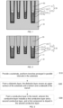
- an embodiment of the present disclosure provides a semiconductor structure, including a substrate 10 and a WL structure 20.
- the substrate 10 includes trenches 11 arranged in parallel intervals.
- the WL structure 20 is located in the trenches 11, and includes a dielectric layer 21 and a conductive layer 22.
- the dielectric layer 21 covers a bottom surface and a sidewall of the conductive layer 22.
- the conductive layer 22 includes a first conductive layer 221 and a second conductive layer 222. A first component is doped in the second conductive layer 222.
- the semiconductor structure in the above embodiment can reduce GIDL caused by the WL structure 20. Moreover, by doping the first component in the second conductive layer 222, the semiconductor structure reduces the work function of the second conductive layer 222 and weakens repulsion of the second conductive layer 222 to electrons, which can further reduce the GIDL caused by the WL structure 20, alleviate the leakage problem in the semiconductor device and lower the power consumption.
- the substrate 10 may include, but is not limited to, a silicon substrate 10.
- the substrate 10 includes active regions and shallow trench isolation (STI) structures arranged in arrays.
- the active regions are located between adjacent ones of the STI structures.
- the trenches 11 are intersected with the active regions and the STI structures.
- the WL structure 20 is located in the trenches 11.
- the dielectric layer 21 covers the bottom surface and the sidewall of the conductive layer 22 to isolate the conductive layer 22 from the active regions.
- the dielectric layer 21 may include, but is not limited to, a High-K material layer such as a silicon dioxide layer.
- the conductive layer 22 includes the first conductive layer 221 and the second conductive layer 222.
- the first component is doped in the second conductive layer 222. By doping the first component in the second conductive layer 222, the semiconductor structure can reduce the work function of the second conductive layer 222, thereby reducing the GIDL of the WL structure 20 and enhancing the gate control capability.
- the second conductive layer 222 is stacked on the first conductive layer 221.
- the second conductive layer 222 includes a horizontal portion and a protrusive portion.
- the protrusive portion is embedded into the first conductive layer 221.
- the first component includes an N-type doping element, such as phosphorus, arsenic or antimony.
- the second conductive layer 222 may include, but is not limited to, a doped polycrystalline silicon layer. After a certain concentration of the N-type doping element is doped in the second conductive layer 222, there is a higher Fermi level. The work function is considered as a difference between the vacuum level and the Fermi level. The work function of the second conductive layer 222 is reduced once the Fermi level is increased.
- the Fermi level is the highest energy level that electrons are filled in a solid energy band at the absolute zero temperature and is commonly represented by EF.
- the vacuum energy is also referred to as a free electron level at which electrons are completely free from the nucleus.
- the first component may have a doping concentration of 18 ⁇ 10 20 cm -3 to 22 ⁇ 10 20 cm -3 , such as 18 ⁇ 10 20 cm -3 , 19 ⁇ 10 20 cm -3 , 20 ⁇ 10 20 cm -3 , 21 ⁇ 10 20 cm -3 or 22 ⁇ 10 20 cm -3 .
- a doping concentration of the first component changes gradually along a thickness direction of the second conductive layer 222.
- the doping concentration of the first component changes stepwise along the thickness direction of the second conductive layer 222.
- the doping concentration of the first component is decreased gradually along the direction from the protrusive portion to the horizontal portion, or the doping concentration of the first component is increased gradually along the direction from the protrusive portion to the horizontal portion.
- the first conductive layer 221 includes a metal layer 221a and a metal barrier layer 221b.
- the metal barrier layer 221b covers a bottom surface and a sidewall of the metal layer 221a, and exposes a top of the metal layer 221a.
- the protrusive portion is embedded into the top of the metal layer 221a.
- a lateral size of the protrusive portion of the second conductive layer 222 is less than that of the horizontal portion of the second conductive layer 222.
- a bottom surface of the horizontal portion contacts a top of the metal barrier layer 221b.
- a sidewall of the horizontal portion of the second conductive layer 222 contacts a part of a sidewall of the dielectric layer 21.
- That part of the dielectric layer 21 is prone to damage when the WL structure is formed by etching, thereby causing the GIDL easily.
- the present disclosure adjusts the work function of the second conductive layer 222 by doping, such that the repulsion of the second conductive layer 222 to the electrons is weakened to reduce the GIDL.
- the metal layer 221a may be a metal conductive material layer with a low resistivity, such as a tungsten layer or a copper layer.
- the metal barrier layer 221b may select a material layer with a barrier function to the metal layer 221a. Furthermore, the metal barrier layer 221b further has a high resistivity, and can be attached well between the semiconductor and the metal.
- the metal barrier layer 221b may include, but is not limited to, a titanium nitride layer, a cobalt layer, a platinum layer or a titanium-tungsten layer.
- the protrusive portion is embedded into the top of the tungsten layer.
- the doped polycrystalline silicon layer includes the horizontal portion and the protrusive portion.
- the horizontal portion is located on the protrusive portion, with the size greater than that of the protrusive portion.
- the bottom surface of the horizontal portion contacts the top of the titanium nitride layer.
- the protrusive portion includes a protrusive surface contacting the top surface of the tungsten layer.
- the semiconductor structure further includes a protective layer 30 located on an upper surface of the second conductive layer 222, and filling up the trenches 11.
- An upper surface of the protective layer 30 is flush with an upper surface of the substrate 10.
- the protective layer 30 may be made of a material including but not limited to silicon nitride or silicon oxynitride. The protective layer 30 can isolate the conductive layer 22 from the outside to protect the conductive layer 22.
- an upper surface of the dielectric layer 21 is flush with the upper surface of the second conductive layer 222.
- the protective layer 30 covers the upper surface of the dielectric layer 21 and the upper surface of the second conductive layer 222.
- the semiconductor structure can prevent the dielectric layer 21 from being damaged by other processes (such as wet etching or dry etching) in subsequent manufacture, and thus makes the device more stable.
- the present disclosure further provides a method of manufacturing a semiconductor structure, including the following steps:
- the first conductive layer 221 and the second conductive layer 222 made of different materials are formed in the trenches 11, and the first conductive layer 221 and the second conductive layer 222 have different work functions, so the method of manufacturing a semiconductor structure reduces GIDL of the WL structure 20. Moreover, by doping the first component in the second conductive layer 222, the method of manufacturing a semiconductor structure reduces the work function of the second conductive layer 222 and weakens repulsion of the second conductive layer 222 to electrons, which can further reduce the GIDL caused by the WL structure 20, alleviate the leakage problem in the semiconductor device and lower the power consumption.
- a plurality of STI structures are formed in the substrate 10 in Step S10.
- the STI structures isolate a plurality of active region (not shown in the figure) arranged in arrays.
- the STI structures may be made of a material including but not limited to silicon oxide and silicon nitride.
- the substrate 10 may include, but is not limited to, a silicon substrate 10.
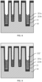
- the step of forming trenches 11 in the substrate 10 includes: Deposit a hard mask layer on the upper surface of the substrate 10, form a pattern in the hard mask layer by patterning, define positions and sizes of the trenches 11, and etch the substrate 10 by photoetching to form the trenches 11 arranged in parallel intervals, as shown in FIG. 4 .
- the trenches 11 are intersected with the active regions and the STI structures.
- the trenches 11 each may have a depth of 50-300 nm, such as 50 nm, 100 nm, 150 nm, 200 nm or 300 nm.
- the trenches 11 each may have a critical dimension (CD) of 20-100 nm, such as 20 nm, 30 nm, 50 nm, 70 nm or 100 nm.
- the trenches 11 each may be provided with a first portion and a second portion.
- the first portion is wider than the second portion.
- the wider first portion is intersected with the active region, and the narrower second portion is intersected with the STI structure.
- Step S20 the dielectric layer 21 is formed, and the dielectric layer 21 covers the bottoms and the sidewalls of the trenches 11 as well as the upper surface of the substrate 10, as shown in FIG. 5 .
- the dielectric layer 21 may include, but is not limited to, a High-K material layer such as a silicon dioxide layer.
- the dielectric layer 21 may be formed on the bottoms and the sidewalls of the trenches 11 as well as on the upper surface of the substrate 10 by in-situ steam generation (ISSG).
- ISSG in-situ steam generation
- the dielectric layer 21 may further be formed by atomic layer deposition (ALD), plasma vapor deposition (PVD) or rapid thermal oxidation (RTO).
- ALD atomic layer deposition
- PVD plasma vapor deposition
- RTO rapid thermal oxidation
- Step S30 the conductive layer 22 is formed in the trenches 11, the conductive layer 22 includes the first conductive layer 221 and the second conductive layer 222, and the first component is doped in the second conductive layer 222, as shown in FIGS. 6-10 .
- the step of forming a conductive layer 22 in the trenches 11 includes:
- Step S31 the step of forming the first conductive layer 221 may include: Step S311: Form a metal barrier material layer 221b', the metal barrier material layer 221b' covering a surface of the dielectric layer 21, as shown in FIG. 6 .
- the metal barrier material layer 221b' may be a material layer with a good barrier function to metal and semiconductor materials, such as a titanium nitride layer, a cobalt layer, a platinum layer or a titanium-tungsten layer.
- the metal barrier material layer 221b' may further have a high resistivity, and is attached well between the semiconductor and the metal.
- the metal barrier material layer 221b' may be formed by chemical vapor deposition (CVD), ALD, PVD or RTO.
- S312 Form a metal material layer 221a', the metal material layer 221a' covering a surface of the metal barrier material layer 221b', and filling up the trenches 11, as shown in FIG. 7 .
- the metal material layer 221a' may be made of a metal conductive material with a low resistivity, including but not limited to tungsten (W), molybdenum (Mo), titanium (Ti), copper (Cu) or gold (Au).
- the metal material layer 221a' may be formed on the surface of the metal barrier material layer 221b' by CVD, and the formed metal material layer 221a' fills up the trenches 11.
- S313 Remove a part of the metal material layer 221a' and a part of the metal barrier material layer 221b' to form the metal layer 221 and the metal barrier layer 221b, thereby obtaining the first conductive layer 221, as shown in FIG. 8 .
- the part of the metal material layer 221a' and the part of the metal barrier material layer 221b' may be removed by etching.
- the metal material layer 221a' and the metal barrier material layer 221b' on the substrate 10 may be removed by dry etching.
- the metal material layer 221a' and the metal barrier material layer 221b' are etched continuously until a distance from a top surface of each of the metal material layer 221a' and the metal barrier material layer 221b' to a top surface of the active region reaches a first preset distance.
- the first preset distance may be 75-85 nm, such as 75 nm, 80 nm or 85 nm.
- any distance from the top surface of each of the metal material layer 221a' and the metal barrier material layer 221b' to the top surface of the active region within 75-85 nm meets the requirements of the present disclosure and will not be listed herein.
- the channel length can be controlled within a reasonable range, and thus the gate control capability can be improved.
- an etching rate to the metal material layer 221a' can be increased by adjusting an etch selectivity of an etching gas to each of the metal material layer 221a' and the metal barrier material layer 221b', thereby forming an arc recess in a top surface of the first conductive layer 221, as shown in FIG. 8 .
- a gas having a high etching rate to the metal material layer 221a' can be charged near the end of the etching.
- the metal material layer 221a' is a tungsten layer
- the metal barrier material layer 221b' is a titanium nitride layer
- chlorine (Cl 2 ) is charged to the chamber near the end of the dry etching.
- the chlorine has a faster etching rate to the tungsten layer than other materials
- the top of the tungsten layer is recessed downward with the continuation of the etching to form the arc recess gradually.
- the depth or shape of the arc recess may be controlled by controlling the charging occasion, charging rate and charging time of the chlorine.
- a protrusive portion protruding downward may be formed in the second conductive layer 222 when the second conductive layer 222 is formed on the upper surface of the first conductive layer, thereby increasing a contact area between the second conductive layer and the first conductive layer.
- Step S32 the step of forming the second conductive layer 222 includes:
- the second conductive material layer 222' may include, but is not limited to, a doped polycrystalline silicon layer.
- the second conductive material layer 222' may be formed by CVD, ALD or PVD.
- the second conductive material layer 222' may be generated on the upper surface of the first conductive layer 221 and the surface of the dielectric layer 21 by low-pressure CVD (LPCVD).
- the device to be used may be a furnace tube, and may also be a chamber device or other devices in single-chip operation.
- the LPCVD in the furnace tube has the advantages of low deposition temperature, easily controllable thin-film component and thickness, direct proportionality between the thin-film thickness and the deposition time, good uniformity and repeatability, good step coverage capability, convenience in operation, etc.
- the first component may be charged to the furnace tube, thereby forming the first component doped polycrystalline silicon layer.
- the first component may be, for example, an N-type doping element such as phosphorus, arsenic or antimony.
- the step of manufacturing the doped polycrystalline silicon layer with the furnace tube may include: Place the substrate 10 into the furnace tube, and charge silane and phosphorane to the furnace tube, phosphorus decomposed from the phosphorane being doped in silicon.
- the polycrystalline silicon layer is generated mainly based on the following chemical formula: SiH 4 (g) ⁇ Si(s)+2H 2 (g).
- the phosphorane is decomposed based on the following formula: PH 3 (phosphorane) ⁇ P+3H.
- the phosphorus decomposed from the phosphorane is doped in the silicon decomposed from the silane.
- the silane is charged to the furnace tube at a flow rate of 200 sccm to 20,000 sccm
- the phosphorane is charged to the furnace tube at a flow rate of 10 sccm to 500 sccm.
- the silane is decomposed into a plurality of particles, atoms, free radicals and ions. These particles are deposited on the substrate 10 through a series of complex processes such as migration and dehydrogenation.
- the polycrystalline silicon layer is deposited at 400-600°C.
- the heating furnace tube is available for batch deposition, in which hundreds of wafers (such as 100 wafers, 150 wafers or 200 wafers) can be placed on the vertical wafer boat at a time. Within set time, a fixed amount of reactive gas is charged to the reaction furnace from the bottom of the reaction chamber of the heating furnace tube or from the ejection quartz tube.
- the doped polycrystalline silicon layer can be simultaneously deposited on all surfaces of the wafers at a set temperature. Exemplarily, as shown in FIG. 9 , the doped polycrystalline silicon layer fills up the trenches 11, and covers the surface of the dielectric layer 21 on the substrate 10.
- the first component may have a doping concentration of 18 ⁇ 10 20 cm -3 to 22 ⁇ 10 20 cm -3 , such as 18 ⁇ 10 20 cm -3 , 19 ⁇ 10 20 cm -3 , 20 ⁇ 10 20 cm -3 , 21 ⁇ 10 20 cm -3 or 22 ⁇ 10 20 cm -3 .
- Any doping concentration of the first component within the range of 18 ⁇ 10 20 cm -3 to 22 ⁇ 10 20 cm -3 meets the requirements of the present disclosure, and will not be listed herein.
- a doping concentration of the first component at different positions in the second conductive material layer 222' may be adjusted by adjusting a rate for charging the first component, such that the doping concentration of the first component changes gradually along a thickness direction of the second conductive material layer 222'.
- the silane is charged to the furnace tube to serve as a silicon source
- the phosphorane is charged to the furnace tube to serve as a phosphorus source.
- the phosphorane is charged to the device at a flow rate of 500 sccm during an early growth stage of the polycrystalline silicon layer.
- the rate for charging the first component is decreased gradually.
- the phosphorane is charged at a flow rate of 50 sccm by the end of the growth of the polycrystalline silicon layer. During the growth, the flow rate for charging the phosphorane is decreased uniformly.
- the first component may further be charged to the furnace tube at a low rate.
- the rate for charging the first component is increased gradually.
- the phosphorane is charged to the device at a flow rate of 50 sccm during the early growth stage of the polycrystalline silicon layer.
- the rate for charging the first component is increased gradually.
- the phosphorane is charged at a flow rate of 500 sccm by the end of the growth of the polycrystalline silicon layer. During the growth, the flow rate for charging the phosphorane is increased uniformly.
- the first component may further be charged to the furnace tube at a low rate.
- the rate for charging the first component is increased gradually.
- a maximum of the doping concentration is preset. Once the doping concentration reaches the maximum, the rate for charging the first component is decreased gradually.
- the doping concentration of the first component in the second conductive layer is increased first and then decreased.
- the first component may further be charged to the furnace tube at a high rate.
- the rate for charging the first component is decreased gradually.
- a minimum of the doping concentration is preset. Once the doping concentration reaches the minimum, the rate for charging the first component is increased gradually.
- the doping concentration of the first component in the second conductive layer is decreased first and then increased.
- the work function of the polycrystalline silicon layer may change by performing N-type doping on the polycrystalline silicon layer.
- the work function is defined as minimum energy required to move an electron from the inside of the object to the surface of the object. A larger work function means that the electron is harder to leave the object.
- Elements for performing the N-type doping on the second conductive layer may include: one or a combination of arsenic, phosphorus and antimony.
- the work function of the second conductive layer may also be adjusted by doping various elements, thereby improving the GIDL effect of the gate structure.
- the second conductive material layer 222' on the substrate 10 may be removed by etching.
- the second conductive material layer 222' in the trenches 11 is etched continuously to make the second conductive material layer 222' thin, until a distance from the top surface of the second conductive material layer 222' to the upper surface of the active region reaches a second preset distance, thereby obtaining the second conductive layer 222.
- the second preset distance may be 55-65 nm, such as 55 nm, 60 nm or 65 nm. Any distance from the top surface of the second conductive material layer 222' to the upper surface of the active region within 55-65 nm meets the requirements of the present disclosure and will not be listed herein.
- the obtained second conductive layer 222 has a uniform doping concentration. If the rate for charging the first component changes (is increased or decreased) as the polycrystalline silicon layer becomes thicker, the doping concentration of the first component in the second conductive layer 222 changes gradually along the thickness direction. Exemplarily, as shown in FIG. 10 , an upper surface of the second conductive layer 222 is lower than the upper surface of the substrate 10.
- the method of manufacturing a semiconductor structure further includes: S40: Form a protective layer 30, the protective layer 30 covering the upper surface of the second conductive layer 222 and the surface of the dielectric layer 21, and filling up the trenches 11, as shown in FIG. 11 .
- the protective layer 30 may be a High-K material layer, such as a silicon nitride layer or a silicon oxynitride layer.
- the protective layer 30 may be formed by ALD or PVD.
- the protective layer 30 covers the upper surface of the second conductive layer 222, and fills up the trenches 11.
- the protective layer 30 may be formed by LPCVD in the furnace tube.
- the protective layer 30 generated in the furnace tube has the desirable uniformity and compactness.
- the protective layer 30 is formed on the upper surface of the second conductive layer 222.
- the protective layer 30 fills up the trenches 11, and extends to the substrate 10.
- the protective layer 30 and the dielectric layer 21 may be planarized by wet etching, dry etching, chemical mechanical polishing (CMP) or lateral etching along the thickness direction, until the upper surface of the substrate 10 is exposed, as shown in FIG. 1 . Both the upper surface of the dielectric layer 21 and the upper surface of the protective layer 30 are flush with the upper surface of the substrate 10.
- the protective layer 30 can isolate the conductive layer 22 from the outside to protect the conductive layer 22.
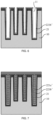
- the present disclosure further provides a direction of manufacturing a semiconductor structure, to form the semiconductor structure shown in FIG. 2 .
- the method includes Step S10, Step S20, Step S30 and Step 40 in the above embodiment, and differs from the above method in: before Step S40, the dielectric layer 21 exposed in the trenches 11 is removed, as shown in FIG. 12 .
- the dielectric layer 21 exposed in the trenches 11 may be removed by dry etching.
- the dielectric layer 21 on inner walls of the trenches 11 is etched directionally with plasma etching to expose sidewalls of the active regions.
- the top surface of the dielectric layer 21 is flush with the upper surface of the second conductive layer 222.
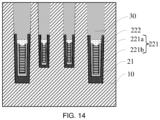
- the dielectric layer 21 in order to prevent a situation wherein the dielectric layer 21 is over etched such that the top surface of the dielectric layer 21 is lower than the upper surface of the second conductive layer 222, only a part of the dielectric layer 21 exposed in the trenches 11 may be removed, such that the top surface of the dielectric layer 21 is higher than the upper surface of the second conductive layer 222 but lower than the upper surface of the substrate 10, as shown in FIG. 13 .
- the process margin can be improved.
- the dielectric layer 21 on the sidewalls of the trenches 11 is etched, the dielectric layer 21 on two sides of the second conductive layer 222 is not damaged in case of over-etching to ensure electrical properties of the WL structure 20.
- the protective layer 30 is formed with the method in Step 40, thereby obtaining the semiconductor structure shown in FIG. 2 or the semiconductor structure shown in FIG. 14 .
- the protective layer 30 may be, for example, a silicon nitride layer or a silicon oxynitride layer. Since the protective layer 30 completely covers the WL structure 20 in the substrate 10, the WL structure 20 is not damaged when other processes are performed on the substrate 10, making the device more stable and reliable.
- the WL structure 20 manufactured with the above method may be referred to as a buried WL structure 20, and includes the first conductive layer 221 and the second conductive layer 222 made of different materials.
- the method of manufacturing a semiconductor structure reduces the GIDL caused by the buried WL structure 20.
- the method of manufacturing a semiconductor structure reduces the work function of the second conductive layer 222, and weakens the repulsion of the second conductive layer 222 to the electrons, which further reduces the GIDL caused by the buried WL structure 20, lowers the power consumption, and improves the gate control capability.
- Step S30 may include Step S31 and Step S32.
- Step S31 may further include Step S311, Step S312 and Step S313.
- the steps or stages are unnecessarily executed at the same time, but may be executed at different times.
- the steps or stages are unnecessarily carried out sequentially, but may be executed alternately with other steps or at least some of steps or stages of other steps.
- the semiconductor structure may be applied to the DRAM or other semiconductor devices.
- the leakage current in the DRAM can be reduced greatly to lower the power consumption.
Landscapes
- Engineering & Computer Science (AREA)
- Manufacturing & Machinery (AREA)
- Semiconductor Memories (AREA)
- Electrodes Of Semiconductors (AREA)
Applications Claiming Priority (2)
| Application Number | Priority Date | Filing Date | Title |
|---|---|---|---|
| CN202210247624.8A CN116801608A (zh) | 2022-03-14 | 2022-03-14 | 半导体结构及其制备方法 |
| PCT/CN2022/082546 WO2023173458A1 (zh) | 2022-03-14 | 2022-03-23 | 半导体结构及其制备方法 |
Publications (2)
| Publication Number | Publication Date |
|---|---|
| EP4270446A1 true EP4270446A1 (de) | 2023-11-01 |
| EP4270446A4 EP4270446A4 (de) | 2023-12-13 |
Family
ID=87931559
Family Applications (1)
| Application Number | Title | Priority Date | Filing Date |
|---|---|---|---|
| EP22764291.5A Pending EP4270446A4 (de) | 2022-03-14 | 2022-03-23 | Halbleiterstruktur und herstellungsverfahren dafür |
Country Status (2)
| Country | Link |
|---|---|
| US (1) | US12356607B2 (de) |
| EP (1) | EP4270446A4 (de) |
Family Cites Families (8)
| Publication number | Priority date | Publication date | Assignee | Title |
|---|---|---|---|---|
| KR101903479B1 (ko) * | 2012-08-24 | 2018-10-02 | 에스케이하이닉스 주식회사 | 반도체 소자 및 그 형성 방법 |
| KR101987995B1 (ko) * | 2012-08-31 | 2019-06-11 | 에스케이하이닉스 주식회사 | 매립 게이트형 반도체 소자, 그 반도체 소자를 갖는 모듈 및 시스템 그리고 그 반도체 소자 제조 방법 |
| KR102336033B1 (ko) | 2015-04-22 | 2021-12-08 | 에스케이하이닉스 주식회사 | 매립금속게이트구조를 구비한 반도체장치 및 그 제조 방법, 그를 구비한 메모리셀, 그를 구비한 전자장치 |
| CN108987282B (zh) | 2018-09-11 | 2023-07-21 | 长鑫存储技术有限公司 | 一种半导体器件及其制造方法 |
| CN110896077B (zh) * | 2018-09-13 | 2024-12-06 | 长鑫存储技术有限公司 | 半导体器件及其制备方法 |
| CN209312720U (zh) | 2019-01-30 | 2019-08-27 | 长鑫存储技术有限公司 | 半导体结构 |
| CN210640255U (zh) * | 2019-11-29 | 2020-05-29 | 长鑫存储技术有限公司 | 半导体器件 |
| CN112331651B (zh) | 2020-11-04 | 2022-05-03 | 福建省晋华集成电路有限公司 | 半导体结构及其制备方法 |
-
2022
- 2022-03-23 EP EP22764291.5A patent/EP4270446A4/de active Pending
- 2022-06-08 US US17/805,923 patent/US12356607B2/en active Active
Also Published As
| Publication number | Publication date |
|---|---|
| US20230292493A1 (en) | 2023-09-14 |
| EP4270446A4 (de) | 2023-12-13 |
| US12356607B2 (en) | 2025-07-08 |
Similar Documents
| Publication | Publication Date | Title |
|---|---|---|
| US7883966B2 (en) | Memory device and method for manufacturing the same | |
| CN103050407B (zh) | 嵌入式晶体管 | |
| US11569240B2 (en) | Semiconductor structure and manufacturing method thereof | |
| WO2007014038A2 (en) | Split gate storage device including a horizontal first gate and a vertical second gate in a trench | |
| CN111564442A (zh) | 半导体结构及制备方法 | |
| EP3933889B1 (de) | Verfahren zur herstellung eines vergrabenen gates und verfahren zur herstellung eines halbleiterbauelements | |
| US8247298B2 (en) | Method of manufacturing semiconductor device | |
| US12114485B2 (en) | Semiconductor structure and method for manufacturing same | |
| US6204115B1 (en) | Manufacture of high-density pillar memory cell arrangement | |
| US7402487B2 (en) | Process for fabricating a semiconductor device having deep trench structures | |
| CN114927523A (zh) | 半导体结构及半导体结构的制备方法 | |
| EP4270446A1 (de) | Halbleiterstruktur und herstellungsverfahren dafür | |
| JP2026512449A (ja) | 4f2のための超薄型ボディアレイトランジスタ | |
| CN116801608A (zh) | 半导体结构及其制备方法 | |
| CN113097302B (zh) | 晶体管及其制作方法 | |
| WO2024077703A1 (zh) | 半导体结构及其制作方法 | |
| JP2013030698A (ja) | 半導体装置の製造方法 | |
| TWI915940B (zh) | Dram及其形成方法 | |
| US12327592B2 (en) | Vertical memory devices and methods for operating the same | |
| CN112151363B (zh) | 具有掺杂表面的设备以及使用原位掺杂的相关方法 | |
| TW202504440A (zh) | 具有降低浮體效應的4f2垂直存取電晶體 | |
| CN115064498A (zh) | 半导体结构的制造方法及半导体结构 | |
| TW202523064A (zh) | 用於4f的雙功函數字線 | |
| CN117794236A (zh) | 半导体结构的制造方法和半导体结构 | |
| CN120076331A (zh) | 分栅存储器及其形成方法 |
Legal Events
| Date | Code | Title | Description |
|---|---|---|---|
| STAA | Information on the status of an ep patent application or granted ep patent |
Free format text: STATUS: UNKNOWN |
|
| STAA | Information on the status of an ep patent application or granted ep patent |
Free format text: STATUS: THE INTERNATIONAL PUBLICATION HAS BEEN MADE |
|
| PUAI | Public reference made under article 153(3) epc to a published international application that has entered the european phase |
Free format text: ORIGINAL CODE: 0009012 |
|
| STAA | Information on the status of an ep patent application or granted ep patent |
Free format text: STATUS: REQUEST FOR EXAMINATION WAS MADE |
|
| 17P | Request for examination filed |
Effective date: 20220912 |
|
| AK | Designated contracting states |
Kind code of ref document: A1 Designated state(s): AL AT BE BG CH CY CZ DE DK EE ES FI FR GB GR HR HU IE IS IT LI LT LU LV MC MK MT NL NO PL PT RO RS SE SI SK SM TR |
|
| REG | Reference to a national code |
Ref country code: DE Ref legal event code: R079 Free format text: PREVIOUS MAIN CLASS: H99Z9999999999 Ipc: H10B0012000000 |
|
| RIN1 | Information on inventor provided before grant (corrected) |
Inventor name: SHI, ZHICHENG Inventor name: LU, YONG Inventor name: HSIEH, MING-HUNG Inventor name: LI, RENHU |
|
| A4 | Supplementary search report drawn up and despatched |
Effective date: 20231114 |
|
| RIC1 | Information provided on ipc code assigned before grant |
Ipc: H10B 12/00 20230101AFI20231108BHEP |
|
| DAV | Request for validation of the european patent (deleted) | ||
| DAX | Request for extension of the european patent (deleted) |