EP4273908A1 - Procédé de fabrication d'un module de dispositif àsemi-conducteurs avec une fiabilité accrue et module de dispositif à semi-conducteurssemi-conducteur - Google Patents
Procédé de fabrication d'un module de dispositif àsemi-conducteurs avec une fiabilité accrue et module de dispositif à semi-conducteurssemi-conducteur Download PDFInfo
- Publication number
- EP4273908A1 EP4273908A1 EP22171599.8A EP22171599A EP4273908A1 EP 4273908 A1 EP4273908 A1 EP 4273908A1 EP 22171599 A EP22171599 A EP 22171599A EP 4273908 A1 EP4273908 A1 EP 4273908A1
- Authority
- EP
- European Patent Office
- Prior art keywords
- encapsulant
- layer
- semiconductor device
- opening
- core layer
- Prior art date
- Legal status (The legal status is an assumption and is not a legal conclusion. Google has not performed a legal analysis and makes no representation as to the accuracy of the status listed.)
- Pending
Links
Images


Classifications
-
- H—ELECTRICITY
- H10—SEMICONDUCTOR DEVICES; ELECTRIC SOLID-STATE DEVICES NOT OTHERWISE PROVIDED FOR
- H10W—GENERIC PACKAGES, INTERCONNECTIONS, CONNECTORS OR OTHER CONSTRUCTIONAL DETAILS OF DEVICES COVERED BY CLASS H10
- H10W74/00—Encapsulations, e.g. protective coatings
- H10W74/01—Manufacture or treatment
-
- H—ELECTRICITY
- H10—SEMICONDUCTOR DEVICES; ELECTRIC SOLID-STATE DEVICES NOT OTHERWISE PROVIDED FOR
- H10W—GENERIC PACKAGES, INTERCONNECTIONS, CONNECTORS OR OTHER CONSTRUCTIONAL DETAILS OF DEVICES COVERED BY CLASS H10
- H10W74/00—Encapsulations, e.g. protective coatings
- H10W74/01—Manufacture or treatment
- H10W74/016—Manufacture or treatment using moulds
-
- H—ELECTRICITY
- H10—SEMICONDUCTOR DEVICES; ELECTRIC SOLID-STATE DEVICES NOT OTHERWISE PROVIDED FOR
- H10W—GENERIC PACKAGES, INTERCONNECTIONS, CONNECTORS OR OTHER CONSTRUCTIONAL DETAILS OF DEVICES COVERED BY CLASS H10
- H10W74/00—Encapsulations, e.g. protective coatings
- H10W74/10—Encapsulations, e.g. protective coatings characterised by their shape or disposition
- H10W74/111—Encapsulations, e.g. protective coatings characterised by their shape or disposition the semiconductor body being completely enclosed
- H10W74/114—Encapsulations, e.g. protective coatings characterised by their shape or disposition the semiconductor body being completely enclosed by a substrate and the encapsulations
-
- H—ELECTRICITY
- H10—SEMICONDUCTOR DEVICES; ELECTRIC SOLID-STATE DEVICES NOT OTHERWISE PROVIDED FOR
- H10W—GENERIC PACKAGES, INTERCONNECTIONS, CONNECTORS OR OTHER CONSTRUCTIONAL DETAILS OF DEVICES COVERED BY CLASS H10
- H10W74/00—Encapsulations, e.g. protective coatings
- H10W74/10—Encapsulations, e.g. protective coatings characterised by their shape or disposition
- H10W74/111—Encapsulations, e.g. protective coatings characterised by their shape or disposition the semiconductor body being completely enclosed
- H10W74/121—Encapsulations, e.g. protective coatings characterised by their shape or disposition the semiconductor body being completely enclosed by multiple encapsulations, e.g. by a thin protective coating and a thick encapsulation
-
- H—ELECTRICITY
- H10—SEMICONDUCTOR DEVICES; ELECTRIC SOLID-STATE DEVICES NOT OTHERWISE PROVIDED FOR
- H10W—GENERIC PACKAGES, INTERCONNECTIONS, CONNECTORS OR OTHER CONSTRUCTIONAL DETAILS OF DEVICES COVERED BY CLASS H10
- H10W74/00—Encapsulations, e.g. protective coatings
- H10W74/40—Encapsulations, e.g. protective coatings characterised by their materials
- H10W74/47—Encapsulations, e.g. protective coatings characterised by their materials comprising organic materials, e.g. plastics or resins
- H10W74/473—Encapsulations, e.g. protective coatings characterised by their materials comprising organic materials, e.g. plastics or resins containing a filler
-
- H—ELECTRICITY
- H05—ELECTRIC TECHNIQUES NOT OTHERWISE PROVIDED FOR
- H05K—PRINTED CIRCUITS; CASINGS OR CONSTRUCTIONAL DETAILS OF ELECTRIC APPARATUS; MANUFACTURE OF ASSEMBLAGES OF ELECTRICAL COMPONENTS
- H05K1/00—Printed circuits
- H05K1/18—Printed circuits structurally associated with non-printed electric components
- H05K1/182—Printed circuits structurally associated with non-printed electric components associated with components mounted in printed circuit boards [PCB], e.g. insert-mounted components [IMC]
- H05K1/185—Printed circuits structurally associated with non-printed electric components associated with components mounted in printed circuit boards [PCB], e.g. insert-mounted components [IMC] associated with components encapsulated in the insulating substrate of the PCBs; associated with components incorporated in internal layers of multilayer circuit boards
-
- H—ELECTRICITY
- H10—SEMICONDUCTOR DEVICES; ELECTRIC SOLID-STATE DEVICES NOT OTHERWISE PROVIDED FOR
- H10W—GENERIC PACKAGES, INTERCONNECTIONS, CONNECTORS OR OTHER CONSTRUCTIONAL DETAILS OF DEVICES COVERED BY CLASS H10
- H10W40/00—Arrangements for thermal protection or thermal control
- H10W40/20—Arrangements for cooling
- H10W40/25—Arrangements for cooling characterised by their materials
- H10W40/255—Arrangements for cooling characterised by their materials having a laminate or multilayered structure, e.g. direct bond copper [DBC] ceramic substrates
-
- H—ELECTRICITY
- H10—SEMICONDUCTOR DEVICES; ELECTRIC SOLID-STATE DEVICES NOT OTHERWISE PROVIDED FOR
- H10W—GENERIC PACKAGES, INTERCONNECTIONS, CONNECTORS OR OTHER CONSTRUCTIONAL DETAILS OF DEVICES COVERED BY CLASS H10
- H10W70/00—Package substrates; Interposers; Redistribution layers [RDL]
- H10W70/40—Leadframes
-
- H—ELECTRICITY
- H10—SEMICONDUCTOR DEVICES; ELECTRIC SOLID-STATE DEVICES NOT OTHERWISE PROVIDED FOR
- H10W—GENERIC PACKAGES, INTERCONNECTIONS, CONNECTORS OR OTHER CONSTRUCTIONAL DETAILS OF DEVICES COVERED BY CLASS H10
- H10W74/00—Encapsulations, e.g. protective coatings
- H10W74/10—Encapsulations, e.g. protective coatings characterised by their shape or disposition
-
- H—ELECTRICITY
- H10—SEMICONDUCTOR DEVICES; ELECTRIC SOLID-STATE DEVICES NOT OTHERWISE PROVIDED FOR
- H10W—GENERIC PACKAGES, INTERCONNECTIONS, CONNECTORS OR OTHER CONSTRUCTIONAL DETAILS OF DEVICES COVERED BY CLASS H10
- H10W90/00—Package configurations
- H10W90/701—Package configurations characterised by the relative positions of pads or connectors relative to package parts
- H10W90/731—Package configurations characterised by the relative positions of pads or connectors relative to package parts of die-attach connectors
- H10W90/734—Package configurations characterised by the relative positions of pads or connectors relative to package parts of die-attach connectors between a chip and a stacked insulating package substrate, interposer or RDL
-
- H—ELECTRICITY
- H10—SEMICONDUCTOR DEVICES; ELECTRIC SOLID-STATE DEVICES NOT OTHERWISE PROVIDED FOR
- H10W—GENERIC PACKAGES, INTERCONNECTIONS, CONNECTORS OR OTHER CONSTRUCTIONAL DETAILS OF DEVICES COVERED BY CLASS H10
- H10W90/00—Package configurations
- H10W90/701—Package configurations characterised by the relative positions of pads or connectors relative to package parts
- H10W90/731—Package configurations characterised by the relative positions of pads or connectors relative to package parts of die-attach connectors
- H10W90/736—Package configurations characterised by the relative positions of pads or connectors relative to package parts of die-attach connectors between a chip and a stacked lead frame, conducting package substrate or heat sink
Definitions
- the present disclosure is related to a method for fabricating a semiconductor device module and to a semiconductor device module.
- the current chip embedding process does not fulfil high voltage application requirements.
- the breakdown voltage, ion impurity level (sodium, chlorine, etc.) and the overall other properties of current PCB materials that are used for chip embedding limit the reliability of 650 V (or even below) devices.
- One of the further problems is also the insufficient adhesion of polymer layers like prepreg layers to the core layer of the PCB and of the semiconductor device to the polymer layers and possible local delamination of these components.
- a first aspect of the present disclosure is related to a method for fabricating a semiconductor device module, the method comprising providing a first encapsulant layer and a core layer disposed on the first encapsulant layer wherein the core layer comprises an opening, disposing a semiconductor device in the opening, the semiconductor device comprising a die carrier and a semiconductor die disposed on the die carrier, dispensing an encapsulant onto the semiconductor device, applying a second encapsulant layer onto the encapsulant so that the encapsulant is pressed into the recess, and laminating together the first and second encapsulant layers and the encapsulant.
- a second aspect of the present disclosure is related to a semiconductor device module comprising a core layer comprising an opening, a semiconductor device disposed in the opening, an encapsulant filled into the opening and at least partly embedding the semiconductor device, a first encapsulant layer disposed on a first main face of the core layer, and a second encapsulant layer disposed on a second main face of the core layer, the second main face being opposite to the first main face, wherein the encapsulant comprises one or more exit areas located outside of the opening in intermediate spaces between the core layer and one or both of the first encapsulant layer and the second encapsulant layer.
- a third aspect of the present disclosure is related to a method for fabricating a device module the method comprising providing a first encapsulant layer and a core layer disposed on the first encapsulant layer wherein the core layer comprises an opening, providing a device and covering the device at least in part with an encapsulant, the encapsulant comprising a B-stage compound or another mold compound which comprises reactive or conditioned surfaces, disposing the device with the encapsulant in the opening, applying a second encapsulant layer onto the core layer and the encapsulant in the opening; and laminating together the first and second encapsulant layers and the encapsulant.
- the terms “bonded”, “attached”, “connected”, “coupled” and/or “electrically connected/electrically coupled” are not meant to mean that the elements or layers must directly be contacted together; intervening elements or layers may be provided between the “bonded”, “attached”, “connected”, “coupled” and/or “electrically connected/electrically coupled” elements, respectively.
- the above-mentioned terms may, optionally, also have the specific meaning that the elements or layers are directly contacted together, i.e. that no intervening elements or layers are provided between the "bonded”, “attached”, “connected”, “coupled” and/or “electrically connected/electrically coupled” elements, respectively.
- the word “over” used with regard to a part, element or material layer formed or located “over” a surface may be used herein to mean that the part, element or material layer be located (e.g. placed, formed, deposited, etc.) "indirectly on” the implied surface with one or more additional parts, elements or layers being arranged between the implied surface and the part, element or material layer.
- the word “over” used with regard to a part, element or material layer formed or located “over” a surface may, optionally, also have the specific meaning that the part, element or material layer be located (e.g. placed, formed, deposited, etc.) "directly on", e.g. in direct contact with, the implied surface.
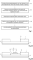
- Fig. 1 shows a flow diagram of an exemplary method for fabricating a semiconductor device module according to the first aspect.
- Fig. 1 shows a method 100 for fabricating a semiconductor device module, the method comprising providing a first encapsulant layer and a core layer disposed on the first encapsulant layer wherein the core layer comprises an opening (110), disposing a semiconductor device in the opening, the semiconductor device comprising a die carrier and a semiconductor die disposed on the die carrier (120), dispensing an encapsulant onto the semiconductor device (130), applying a second encapsulant layer onto the encapsulant so that the encapsulant is pressed into the opening (140), and laminating together the first and second encapsulant layers and the encapsulant (150).
- Fig. 2 comprises Fig. 2A to 2E and shows schematic cross-sectional side view representations for illustrating an example of an exemplary method for fabricating a semiconductor device module according to the first aspect.
- Fig. 2A shows an intermediate product comprising a core layer 1 comprising a recess or opening 1A, the core layer 1 being disposed on a first encapsulant layer 4.
- the core layer 1 can, for example, comprise an FR1, FR2, FR3, or FR4 material, a BT-Epoxy (where BT stands for bismaleimidtriazine), a polyimide, or a cyanate ester.
- the first encapsulant layer 4 may comprise a first polymer, in particular a first prepreg layer 4.
- a first Cu layer 6 may be disposed on a rear surface of the first encapsulant layer 4 remote from the core layer 1.
- Fig. 2B shows an intermediate product after placing a semiconductor device 2 into the opening 1A of the core layer 1.
- the semiconductor device 2 comprises a die carrier 2.1, and a semiconductor die 2.2 attached to the die carrier 2.1.
- the semiconductor device 2 can be non-isolated wherein the die carrier 2.1 can be a leadframe, a copper block etc.
- the semiconductor device 2 can also be isolated e.g. like a DCB (direct copper bond), an AMB (active metal braze, an IMS (insulated metal substrate), or a pre-laminated package or a fullpack (isolated by thermal conductive encapsulant) .
- the semiconductor die 2.2 may comprise a semiconductor transistor die 2.2 like, e.g. one or more of an IGBT, a MOSFET die, a CoolMOS, or a wide band gap semiconductor transistor like SiC-MOS, or GaN-MOS.
- the semiconductor transistor die 2.2 may comprise a contact pad 2.2A on an upper surface thereof, which contact pad 2.2A can be, for example, a source pad 2A. Further contact pads may be arranged on the upper surface of the semiconductor transistor die 2.2 like, e.g., a gate pad or a source sense pad.
- a semiconductor component instead of a semiconductor component, another component can also be installed in the module in the manner described.
- a passive component such as a diode, a capacitor or a resistor can be used.
- a heat sink in the form of a copper insert can be used.
- a conductor rail or bus bar is also conceivable for use.
- Fig. 2C shows an intermediate product after dispensing an encapsulant 3 onto the semiconductor device.
- the encapsulant 3 comprises a material which can in general be a material out of the group of adhesives like, for example, a duromer, an elastomer or a thermoplastic.
- the encapsulant 3 can also be one or more of a liquid mold compound, a resin, an organic resin, an epoxy resin, an inorganic resin, a polyimide, a cyanate ester, a silicone, or mixtures of the above components.
- the encapsulant 3 can also be made of one of the above mentioned materials and furthermore being filled with special filler particles, e.g. for instance comprising or consisting of metal oxide or metal nitride filler particles, in particular AlO, SiO, ZrO 2 , Si 3 N 4 , BN, AlN, or diamond.
- special filler particles e.g. for instance comprising or consisting of metal oxide or metal nitride filler particles, in particular AlO, SiO, ZrO 2 , Si 3 N 4 , BN, AlN, or diamond.
- Fig. 2D shows an intermediate product immediately after a first stage of applying a second encapsulant layer 5 onto the core layer 1 and the encapsulant 3 and simultaneously laminating together the first and second encapsulant layers 4 and 5 and the encapsulant 3.
- the application of the second encapsulant layer 5 results in that the encapsulant 3 is pressed into the opening 1A and embeds the semiconductor device 2.
- This process step therefore involves laminating of the first and second encapsulant layers 4 and 5, which additionally includes compression molding properties.
- the two encapsulant layers 4 and 5 are connected with each other.
- the second encapsulant layer 5 may comprise a polymer layer, in particular a prepreg layer 5 and have a copper layer 7 on its surface facing away from the core layer 1.
- the copper layer 7 comprises conductive areas or traces which are connected by electrical vias in the second encapsulant layer 5 with the contacts pads of the semiconductor die.
- the electrical vias can be fabricated by laser drilling and subsequent filling of the vias with copper by chemical galvanic plating.
- the encapsulant layers 4 and 5 can both contain standard filler particles, e.g. SiO, but also thermal conductive filler particles, e.g. Al2O3, BrN etc.
- the encapsulant layers 4 and 5 can have different properties, wherein most likely is that the second encapsulant layer 5 contains standard fillers, and the first encapsulant layer 4 contains thermal conductive fillers for proper heat dissipation.
- Fig. 2E shows a semiconductor device module after completion of the combined laminating and compression molding step. It can be seen that the encapsulant 3 has been filled into the space of the opening 1A which is not occupied by the semiconductor device 2. Moreover, it can be seen that the encapsulant 3 not only completely fills the opening 1A but has partially flowed out of the opening 1A during the compression molding step to form exit areas 3A located outside of the opening 1A in intermediate spaces between the core layer 1 the first and second encapsulant layers 4 and 5. In the embodiment shown in Fig. 2E , exit areas 3A of the encapsulant 3 are shown between the core layer 1 and both the first and second encapsulant layers 4 and 5. However, it is just as possible that these exit areas 3A only occur at isolated points between the core layer 1 and one or both of the two encapsulant layers 4 or 5.
- the previously dispensed encapsulant 3 flows into the opening 1A, i.e. into the area of the opening 1A which is not occupied by the semiconductor device 2.
- materials contained in the second encapsulant layer 5 may flow out of the second encapsulant layer 5 into the opening 1A.
- resin material contained in the prepreg layer may flow out of the prepreg layer into the opening 1A.
- Fig. 3 shows a flow diagram of an exemplary method for fabricating a device module according to the third aspect.
- the method 200 as shown in Fig. 3 comprises providing a first encapsulant layer and a core layer disposed on the first encapsulant layer wherein the core layer comprises an opening (210), providing a device and covering the device at least in part with an encapsulant, the encapsulant comprising a B-stage mold compound or another mold compound which comprises reactive or conditioned surfaces (220), disposing the device with the encapsulant in the opening (230), applying a second encapsulant layer onto the core layer and the encapsulant in the opening (240), and laminating together the first and second encapsulant layers and the encapsulant (250).
- Fig. 4 comprises Fig. 4A to 4D and shows schematic cross-sectional side view representations of intermediate products and a semiconductor device module for illustrating an example of an exemplary method for fabricating a semiconductor device module according to the third aspect.
- Fig. 4A shows an intermediate product comprising a core layer 1 comprising a recess or opening 1A, the core layer 1 being disposed on a first encapsulant layer 4.
- the core layer 1 can, for example, comprise a FR1, FR2, FR3, or FR4 material, a BT-epoxy (where BT stands for bismaleimidtriazine), a polyimide, a cyanate ester, or a glass substrate.
- the core layer 1 can further comprise an organic material, an inorganic material, an electrically insulating or an electrically conductive material, in particular copper or aluminum.
- the first encapsulant layer 4 may comprise a first prepreg layer 4.
- a first Cu layer 6 may be disposed on a rear surface of the first encapsulant layer 4 remote from the core layer 1.
- Fig. 4B shows an intermediate product after providing a semiconductor device 2 and covering the semiconductor device 2 at least in part with an encapsulant 23, the encapsulant 23 comprising a B-stage mold compound.
- the semiconductor device 2 comprises a die carrier 2.1, and a semiconductor die 2.2 attached to the die carrier 2.1.
- the semiconductor device 2 can be non-isolated wherein the die carrier 2.1 can be a leadframe, a copper block etc.
- the semiconductor device 2 can also be isolated e.g. like a DCB (direct copper bond), an AMB (active metal braze, an IMS (insulated metal substrate), or a pre-laminated package or a fullpack (isolated by thermal conductive encapsulant).
- the semiconductor die 2.2 may comprise a semiconductor transistor die 2.2 like, e.g. one or more of an IGBT, a MOSFET die, a CoolMOS, or a wide band gap semiconductor transistor like SiC-MOS, or GaN-MOS.
- the semiconductor transistor die 2.2 may comprise a contact pad 2.2A on an upper surface thereof, which contact pad 2.2A can be, for example, a source pad 2A. Further contact pads may be arranged on the upper surface of the semiconductor transistor die 2.2 like, e.g., a gate pad or a source sense pad.
- the encapsulant 23 comprises an electrically insulating B stage compound which can be one or more of a resin, an epoxy resin, a duroplast, a polyimide, a BMI (bismaleimide), a silicone, a cyanate ester, or mixtures of the above.
- a B stage compound is in general a system wherein the reaction between the compound and the curing agent/hardener is not complete. Due to this, the system is in a partially cured stage. When this system is later reheated at elevated temperatures, the cross-linking is complete and the system fully cures.
- the degree of cure of the B stage epoxy compound 23 can, for example, be in a range from 20% to 60%, more specifically from 50% to 70% on average. In particular, at the main surfaces of the B-stage epoxy compound 23 the degree of cure can be less than at a center region. As can be seen in Fig. 4B , the low degree of cure leads to a frayed and structured surface of the epoxy compound 23.
- the B stage epoxy compound can be applied to the semiconductor device by transfer molding or compression molding, or other forming processes like printing, in particular 3D printing, or dispensing. In any case the forming process can be performed so that also on a lower surface of the die carrier 2.1 a thin layer of mold compound 23 can be applied which then also comprises a frayed and structured surface.
- Fig. 4C shows an intermediate product after inserting the semiconductor device 2 together with the encapsulant 23 into the opening 1A of the core layer 1.
- the background to the use of a B-stage compound is as follows. A fully polymerized epoxy resin material results in slick surfaces which are unfavorable for adhesion to adjacent layers and can lead to delamination. Use of B stage mold material can solve this problem.
- the mold material in the lamination tool gets fluid and can intermix with both the first and second laminate layers 4 and 5. Active groups can undergo cross linking with the first and second polymer layers 4 and 5 and so improve adhesion.
- Fig. 4D shows a semiconductor device module after laminating the second polymer layer 5 onto the core layer 1 and the encapsulant 23 in the opening 1A.
- the encapsulant 3 is fully cured after this lamination step.
- a cross-mixed or linked area has formed due to the mixing of the materials, which improves adhesion.
- the second polymer layer 5 may comprise a prepreg layer 5 and have a copper layer 7 on its surface facing away from the core layer 1.
- the copper layer 7 comprises conductive areas or traces which are connected by electrical vias in the second encapsulant layer 5 with the contacts pads of the semiconductor die.
- the electrical vias can be fabricated by laser drilling and subsequent filling of the vias with copper by chemical galvanic plating.
- Example 1 is a method for fabricating a semiconductor device module, the method comprising providing a first encapsulant layer and a core layer disposed on the first encapsulant layer wherein the core layer comprises an opening,-disposing a semiconductor device in the opening, the semiconductor device comprising a die carrier and a semiconductor die disposed on the die carrier, dispensing an encapsulant onto the semiconductor device, applying a second encapsulant layer onto the encapsulant so that the encapsulant is pressed into the opening, and laminating together the first and second encapsulant layers and the encapsulant.
- Example 2 is the method according to Example 1, wherein one or both of the first encapsulant layer and the second encapsulant layer comprises a polymer layer or a prepreg layer, respectively.
- Example 3 is the method according to Example 1 or 2, wherein the core layer comprises one of an FR1, FR2, FR3, or an FR4 material, a BT-epoxy, a polyimide, a cyanate ester, an organic material, an inorganic material, an electrically insulating material, or an electrically conductive material.
- the core layer comprises one of an FR1, FR2, FR3, or an FR4 material, a BT-epoxy, a polyimide, a cyanate ester, an organic material, an inorganic material, an electrically insulating material, or an electrically conductive material.
- Example 4 is the method according to any one of the preceding Examples, wherein the encapsulant comprises a material which is one or more of: one out of the group of adhesives, including a duromer, an elastomer and a thermoplastic, a liquid mold compound, a resin, an organic resin, an epoxy resin, an inorganic resin, a granulate, a polyimide, a silicone, a cyanate ester, or mixtures of the above components.
- the encapsulant comprises a material which is one or more of: one out of the group of adhesives, including a duromer, an elastomer and a thermoplastic, a liquid mold compound, a resin, an organic resin, an epoxy resin, an inorganic resin, a granulate, a polyimide, a silicone, a cyanate ester, or mixtures of the above components.
- Example 5 is a semiconductor device module, comprising a core layer comprising an opening, a semiconductor device disposed in the opening, an encapsulant filled into the opening and at least partly embedding the semiconductor device, a first encapsulant layer disposed on a first main face of the core layer, and a second encapsulant layer disposed on a second main face of the core layer, the second main face being opposite to the first main face, wherein the encapsulant comprises one or more exit areas located outside of the opening in intermediate spaces between the core layer and one or both of the first polymer layer and the second encapsulant layer.
- Example 6 is the semiconductor device module according to Example 5, wherein one or both of the first encapsulant layer and the second encapsulant layer comprise a polymer layer or a prepreg layer.
- Example 7 is the semiconductor device module according to Example 5 or 6, wherein the core layer comprises one of an FR1, FR2, FR3, or an FR4 material, a BT-epoxy, a polyimide, a cyanate ester, an organic material, an inorganic material, an electrically insulating material, or an electrically conductive material.
- the core layer comprises one of an FR1, FR2, FR3, or an FR4 material, a BT-epoxy, a polyimide, a cyanate ester, an organic material, an inorganic material, an electrically insulating material, or an electrically conductive material.
- Example 8 is the semiconductor device module according to any one of Examples 5 to 7, wherein the encapsulant comprises a material which is one or more of: one out of the group of adhesives, including a duromer, an elastomer and a thermoplastic, a liquid mold compound, a resin, an organic resin, an epoxy resin, an inorganic resin, a granulate, a polyimide, a silicone, a cyanate ester, or mixtures of the above components.
- the encapsulant comprises a material which is one or more of: one out of the group of adhesives, including a duromer, an elastomer and a thermoplastic, a liquid mold compound, a resin, an organic resin, an epoxy resin, an inorganic resin, a granulate, a polyimide, a silicone, a cyanate ester, or mixtures of the above components.
- Example 9 is the semiconductor device module according to any of Examples 5 to 8, further comprising a first copper layer disposed on an outer surface of the first encapsulant layer.
- Example 10 is the semiconductor device module according to any of Examples 5 to 9, further comprising a second copper layer disposed on an outer surface of the second encapsulant layer.
- Example 11 is a method for fabricating a device module, the method comprising providing a first encapsulant layer and a core layer disposed on the first encapsulant layer wherein the core layer comprises an opening, providing a device and covering the device at least in part with an encapsulant, the encapsulant comprising a B-stage mold compound or another mold compound which comprises reactive or conditioned surfaces, disposing the device with the encapsulant in the opening, applying a second encapsulant layer onto the core layer and the encapsulant in the opening, and laminating together the first and second encapsulant layers and the encapsulant.
- Example 12 is the method according to Example 11, wherein the B-stage mold compound comprises a partial polymerization in a range from 20% to 60% or from 50% to 70%.
- Example 13 is the method according to Example 11 or 12, wherein one or both of the first encapsulant layer and the second encapsulant layer comprises a prepreg layer.
- Example 14 is the method according to any one of Examples 11 or 13, wherein the core layer comprises one of an FR1, FR2, FR3, or an FR4 material, a BT-epoxy, a polyimide, a cyanate ester, an organic material, an inorganic material, an electrically insulating material, or an electrically conductive material.
- the core layer comprises one of an FR1, FR2, FR3, or an FR4 material, a BT-epoxy, a polyimide, a cyanate ester, an organic material, an inorganic material, an electrically insulating material, or an electrically conductive material.
- Example 15 is the method according to any one of Examples 11 to 14, wherein the device is one or more of a semiconductor device, a semiconductor transistor device, a passive device, a copper inset, or a bus bar,
- Example 16 is the method according to any one of Examples 11 to 15, wherein the encapsulant comprises another mold compound in which the reactive or conditioned surfaces comprise frayed, structured, roughened, or plasma activated surfaces.
Landscapes
- Structures Or Materials For Encapsulating Or Coating Semiconductor Devices Or Solid State Devices (AREA)
- Engineering & Computer Science (AREA)
- Microelectronics & Electronic Packaging (AREA)
Priority Applications (3)
| Application Number | Priority Date | Filing Date | Title |
|---|---|---|---|
| EP22171599.8A EP4273908A1 (fr) | 2022-05-04 | 2022-05-04 | Procédé de fabrication d'un module de dispositif àsemi-conducteurs avec une fiabilité accrue et module de dispositif à semi-conducteurssemi-conducteur |
| US18/140,976 US20230360929A1 (en) | 2022-05-04 | 2023-04-28 | Method for fabricating a semiconductor device module with increased reliability and a semiconductor device module |
| CN202310491032.5A CN117012655A (zh) | 2022-05-04 | 2023-05-04 | 一种用于制造具有提高的可靠性的半导体器件模块的方法和半导体器件模块 |
Applications Claiming Priority (1)
| Application Number | Priority Date | Filing Date | Title |
|---|---|---|---|
| EP22171599.8A EP4273908A1 (fr) | 2022-05-04 | 2022-05-04 | Procédé de fabrication d'un module de dispositif àsemi-conducteurs avec une fiabilité accrue et module de dispositif à semi-conducteurssemi-conducteur |
Publications (1)
| Publication Number | Publication Date |
|---|---|
| EP4273908A1 true EP4273908A1 (fr) | 2023-11-08 |
Family
ID=81597752
Family Applications (1)
| Application Number | Title | Priority Date | Filing Date |
|---|---|---|---|
| EP22171599.8A Pending EP4273908A1 (fr) | 2022-05-04 | 2022-05-04 | Procédé de fabrication d'un module de dispositif àsemi-conducteurs avec une fiabilité accrue et module de dispositif à semi-conducteurssemi-conducteur |
Country Status (3)
| Country | Link |
|---|---|
| US (1) | US20230360929A1 (fr) |
| EP (1) | EP4273908A1 (fr) |
| CN (1) | CN117012655A (fr) |
Citations (3)
| Publication number | Priority date | Publication date | Assignee | Title |
|---|---|---|---|---|
| US20090218118A1 (en) * | 2008-02-29 | 2009-09-03 | Fujitsu Limited | Board and manufacturing method for the same |
| US20140208588A1 (en) * | 2003-04-01 | 2014-07-31 | Ge Embedded Electronics Oy | Method for manufacturing an electronic module and an electronic module |
| US20180213647A1 (en) * | 2017-01-26 | 2018-07-26 | At & S Austria Technologie & Systemtechnik Aktiengesellschaft | Solid-State Transition Piece Being Transferable Into an Adhesive State for Embedding a Component in a Component Carrier |
Family Cites Families (1)
| Publication number | Priority date | Publication date | Assignee | Title |
|---|---|---|---|---|
| US9610758B2 (en) * | 2007-06-21 | 2017-04-04 | General Electric Company | Method of making demountable interconnect structure |
-
2022
- 2022-05-04 EP EP22171599.8A patent/EP4273908A1/fr active Pending
-
2023
- 2023-04-28 US US18/140,976 patent/US20230360929A1/en active Pending
- 2023-05-04 CN CN202310491032.5A patent/CN117012655A/zh active Pending
Patent Citations (3)
| Publication number | Priority date | Publication date | Assignee | Title |
|---|---|---|---|---|
| US20140208588A1 (en) * | 2003-04-01 | 2014-07-31 | Ge Embedded Electronics Oy | Method for manufacturing an electronic module and an electronic module |
| US20090218118A1 (en) * | 2008-02-29 | 2009-09-03 | Fujitsu Limited | Board and manufacturing method for the same |
| US20180213647A1 (en) * | 2017-01-26 | 2018-07-26 | At & S Austria Technologie & Systemtechnik Aktiengesellschaft | Solid-State Transition Piece Being Transferable Into an Adhesive State for Embedding a Component in a Component Carrier |
Also Published As
| Publication number | Publication date |
|---|---|
| US20230360929A1 (en) | 2023-11-09 |
| CN117012655A (zh) | 2023-11-07 |
Similar Documents
| Publication | Publication Date | Title |
|---|---|---|
| US10242969B2 (en) | Semiconductor package comprising a transistor chip module and a driver chip module and a method for fabricating the same | |
| US9190389B2 (en) | Chip package with passives | |
| US10211158B2 (en) | Power semiconductor module having a direct copper bonded substrate and an integrated passive component, and an integrated power module | |
| US10079195B2 (en) | Semiconductor chip package comprising laterally extending connectors | |
| US9397018B2 (en) | Chip arrangement, a method for manufacturing a chip arrangement, integrated circuits and a method for manufacturing an integrated circuit | |
| US12463116B2 (en) | Method for fabricating a semiconductor device including an embedded semiconductor die | |
| CN103377951B (zh) | 半导体器件的制造方法和半导体器件 | |
| EP4057335A1 (fr) | Boîtier à semi-conducteurs et son procédé de fabrication | |
| US20250174509A1 (en) | Encapsulated package with carrier, laminate body and component in between | |
| CN104051363A (zh) | 芯片封装和用于制造该芯片封装的方法 | |
| CN108346651A (zh) | 包括晶体管芯片、二极管芯片和驱动器芯片的半导体模块 | |
| US12080669B2 (en) | Semiconductor device module having vertical metallic contacts and a method for fabricating the same | |
| US10304751B2 (en) | Electronic sub-module including a leadframe and a semiconductor chip disposed on the leadframe | |
| US9379050B2 (en) | Electronic device | |
| US20230360929A1 (en) | Method for fabricating a semiconductor device module with increased reliability and a semiconductor device module | |
| EP3422824B1 (fr) | Intégration dans une carte à circuit imprimé avec forage | |
| US20230282591A1 (en) | Semiconductor package and a semiconductor device module including the same | |
| US11817407B2 (en) | Molded semiconductor package with high voltage isolation | |
| US20230378011A1 (en) | Electronic device module and a device module both having an adhesion promoter layer | |
| US20240266237A1 (en) | A semiconductor transistor package having electrical contact layers and a method for fabricating the same | |
| US20260005150A1 (en) | Power Module with Multi-Layer Substrate and Second Insulation Layer to Increase Power Density |
Legal Events
| Date | Code | Title | Description |
|---|---|---|---|
| PUAI | Public reference made under article 153(3) epc to a published international application that has entered the european phase |
Free format text: ORIGINAL CODE: 0009012 |
|
| STAA | Information on the status of an ep patent application or granted ep patent |
Free format text: STATUS: THE APPLICATION HAS BEEN PUBLISHED |
|
| AK | Designated contracting states |
Kind code of ref document: A1 Designated state(s): AL AT BE BG CH CY CZ DE DK EE ES FI FR GB GR HR HU IE IS IT LI LT LU LV MC MK MT NL NO PL PT RO RS SE SI SK SM TR |
|
| STAA | Information on the status of an ep patent application or granted ep patent |
Free format text: STATUS: REQUEST FOR EXAMINATION WAS MADE |
|
| 17P | Request for examination filed |
Effective date: 20240507 |
|
| RBV | Designated contracting states (corrected) |
Designated state(s): AL AT BE BG CH CY CZ DE DK EE ES FI FR GB GR HR HU IE IS IT LI LT LU LV MC MK MT NL NO PL PT RO RS SE SI SK SM TR |