EP4273928A1 - Halbleitergehäuse mit leistung und logik auf einer einzelnen keramikplate - Google Patents
Halbleitergehäuse mit leistung und logik auf einer einzelnen keramikplate Download PDFInfo
- Publication number
- EP4273928A1 EP4273928A1 EP22171175.7A EP22171175A EP4273928A1 EP 4273928 A1 EP4273928 A1 EP 4273928A1 EP 22171175 A EP22171175 A EP 22171175A EP 4273928 A1 EP4273928 A1 EP 4273928A1
- Authority
- EP
- European Patent Office
- Prior art keywords
- conductive layer
- semiconductor package
- semiconductor
- ceramic plate
- die
- Prior art date
- Legal status (The legal status is an assumption and is not a legal conclusion. Google has not performed a legal analysis and makes no representation as to the accuracy of the status listed.)
- Pending
Links
Images
Classifications
-
- H—ELECTRICITY
- H10—SEMICONDUCTOR DEVICES; ELECTRIC SOLID-STATE DEVICES NOT OTHERWISE PROVIDED FOR
- H10W—GENERIC PACKAGES, INTERCONNECTIONS, CONNECTORS OR OTHER CONSTRUCTIONAL DETAILS OF DEVICES COVERED BY CLASS H10
- H10W74/00—Encapsulations, e.g. protective coatings
- H10W74/10—Encapsulations, e.g. protective coatings characterised by their shape or disposition
- H10W74/111—Encapsulations, e.g. protective coatings characterised by their shape or disposition the semiconductor body being completely enclosed
-
- H—ELECTRICITY
- H10—SEMICONDUCTOR DEVICES; ELECTRIC SOLID-STATE DEVICES NOT OTHERWISE PROVIDED FOR
- H10W—GENERIC PACKAGES, INTERCONNECTIONS, CONNECTORS OR OTHER CONSTRUCTIONAL DETAILS OF DEVICES COVERED BY CLASS H10
- H10W90/00—Package configurations
-
- H—ELECTRICITY
- H10—SEMICONDUCTOR DEVICES; ELECTRIC SOLID-STATE DEVICES NOT OTHERWISE PROVIDED FOR
- H10W—GENERIC PACKAGES, INTERCONNECTIONS, CONNECTORS OR OTHER CONSTRUCTIONAL DETAILS OF DEVICES COVERED BY CLASS H10
- H10W40/00—Arrangements for thermal protection or thermal control
- H10W40/20—Arrangements for cooling
- H10W40/25—Arrangements for cooling characterised by their materials
- H10W40/255—Arrangements for cooling characterised by their materials having a laminate or multilayered structure, e.g. direct bond copper [DBC] ceramic substrates
-
- H—ELECTRICITY
- H10—SEMICONDUCTOR DEVICES; ELECTRIC SOLID-STATE DEVICES NOT OTHERWISE PROVIDED FOR
- H10W—GENERIC PACKAGES, INTERCONNECTIONS, CONNECTORS OR OTHER CONSTRUCTIONAL DETAILS OF DEVICES COVERED BY CLASS H10
- H10W40/00—Arrangements for thermal protection or thermal control
- H10W40/70—Fillings or auxiliary members in containers or in encapsulations for thermal protection or control
- H10W40/77—Auxiliary members characterised by their shape
- H10W40/778—Auxiliary members characterised by their shape in encapsulations
-
- H—ELECTRICITY
- H10—SEMICONDUCTOR DEVICES; ELECTRIC SOLID-STATE DEVICES NOT OTHERWISE PROVIDED FOR
- H10W—GENERIC PACKAGES, INTERCONNECTIONS, CONNECTORS OR OTHER CONSTRUCTIONAL DETAILS OF DEVICES COVERED BY CLASS H10
- H10W70/00—Package substrates; Interposers; Redistribution layers [RDL]
- H10W70/40—Leadframes
- H10W70/421—Shapes or dispositions
-
- H—ELECTRICITY
- H10—SEMICONDUCTOR DEVICES; ELECTRIC SOLID-STATE DEVICES NOT OTHERWISE PROVIDED FOR
- H10W—GENERIC PACKAGES, INTERCONNECTIONS, CONNECTORS OR OTHER CONSTRUCTIONAL DETAILS OF DEVICES COVERED BY CLASS H10
- H10W70/00—Package substrates; Interposers; Redistribution layers [RDL]
- H10W70/40—Leadframes
- H10W70/481—Leadframes for devices being provided for in groups H10D8/00 - H10D48/00
-
- H—ELECTRICITY
- H10—SEMICONDUCTOR DEVICES; ELECTRIC SOLID-STATE DEVICES NOT OTHERWISE PROVIDED FOR
- H10W—GENERIC PACKAGES, INTERCONNECTIONS, CONNECTORS OR OTHER CONSTRUCTIONAL DETAILS OF DEVICES COVERED BY CLASS H10
- H10W70/00—Package substrates; Interposers; Redistribution layers [RDL]
- H10W70/60—Insulating or insulated package substrates; Interposers; Redistribution layers
-
- H—ELECTRICITY
- H10—SEMICONDUCTOR DEVICES; ELECTRIC SOLID-STATE DEVICES NOT OTHERWISE PROVIDED FOR
- H10W—GENERIC PACKAGES, INTERCONNECTIONS, CONNECTORS OR OTHER CONSTRUCTIONAL DETAILS OF DEVICES COVERED BY CLASS H10
- H10W70/00—Package substrates; Interposers; Redistribution layers [RDL]
- H10W70/60—Insulating or insulated package substrates; Interposers; Redistribution layers
- H10W70/67—Insulating or insulated package substrates; Interposers; Redistribution layers characterised by their insulating layers or insulating parts
- H10W70/69—Insulating materials thereof
- H10W70/692—Ceramics or glasses
-
- H—ELECTRICITY
- H10—SEMICONDUCTOR DEVICES; ELECTRIC SOLID-STATE DEVICES NOT OTHERWISE PROVIDED FOR
- H10W—GENERIC PACKAGES, INTERCONNECTIONS, CONNECTORS OR OTHER CONSTRUCTIONAL DETAILS OF DEVICES COVERED BY CLASS H10
- H10W74/00—Encapsulations, e.g. protective coatings
- H10W74/10—Encapsulations, e.g. protective coatings characterised by their shape or disposition
- H10W74/111—Encapsulations, e.g. protective coatings characterised by their shape or disposition the semiconductor body being completely enclosed
- H10W74/114—Encapsulations, e.g. protective coatings characterised by their shape or disposition the semiconductor body being completely enclosed by a substrate and the encapsulations
-
- H—ELECTRICITY
- H10—SEMICONDUCTOR DEVICES; ELECTRIC SOLID-STATE DEVICES NOT OTHERWISE PROVIDED FOR
- H10W—GENERIC PACKAGES, INTERCONNECTIONS, CONNECTORS OR OTHER CONSTRUCTIONAL DETAILS OF DEVICES COVERED BY CLASS H10
- H10W74/00—Encapsulations, e.g. protective coatings
- H10W74/40—Encapsulations, e.g. protective coatings characterised by their materials
- H10W74/47—Encapsulations, e.g. protective coatings characterised by their materials comprising organic materials, e.g. plastics or resins
- H10W74/473—Encapsulations, e.g. protective coatings characterised by their materials comprising organic materials, e.g. plastics or resins containing a filler
-
- H—ELECTRICITY
- H10—SEMICONDUCTOR DEVICES; ELECTRIC SOLID-STATE DEVICES NOT OTHERWISE PROVIDED FOR
- H10W—GENERIC PACKAGES, INTERCONNECTIONS, CONNECTORS OR OTHER CONSTRUCTIONAL DETAILS OF DEVICES COVERED BY CLASS H10
- H10W90/00—Package configurations
- H10W90/701—Package configurations characterised by the relative positions of pads or connectors relative to package parts
-
- H—ELECTRICITY
- H10—SEMICONDUCTOR DEVICES; ELECTRIC SOLID-STATE DEVICES NOT OTHERWISE PROVIDED FOR
- H10W—GENERIC PACKAGES, INTERCONNECTIONS, CONNECTORS OR OTHER CONSTRUCTIONAL DETAILS OF DEVICES COVERED BY CLASS H10
- H10W90/00—Package configurations
- H10W90/811—Multiple chips on leadframes
-
- H—ELECTRICITY
- H10—SEMICONDUCTOR DEVICES; ELECTRIC SOLID-STATE DEVICES NOT OTHERWISE PROVIDED FOR
- H10W—GENERIC PACKAGES, INTERCONNECTIONS, CONNECTORS OR OTHER CONSTRUCTIONAL DETAILS OF DEVICES COVERED BY CLASS H10
- H10W72/00—Interconnections or connectors in packages
- H10W72/30—Die-attach connectors
- H10W72/351—Materials of die-attach connectors
- H10W72/352—Materials of die-attach connectors comprising metals or metalloids, e.g. solders
-
- H—ELECTRICITY
- H10—SEMICONDUCTOR DEVICES; ELECTRIC SOLID-STATE DEVICES NOT OTHERWISE PROVIDED FOR
- H10W—GENERIC PACKAGES, INTERCONNECTIONS, CONNECTORS OR OTHER CONSTRUCTIONAL DETAILS OF DEVICES COVERED BY CLASS H10
- H10W72/00—Interconnections or connectors in packages
- H10W72/50—Bond wires
- H10W72/541—Dispositions of bond wires
- H10W72/5445—Dispositions of bond wires being orthogonal to a side surface of the chip, e.g. parallel arrangements
-
- H—ELECTRICITY
- H10—SEMICONDUCTOR DEVICES; ELECTRIC SOLID-STATE DEVICES NOT OTHERWISE PROVIDED FOR
- H10W—GENERIC PACKAGES, INTERCONNECTIONS, CONNECTORS OR OTHER CONSTRUCTIONAL DETAILS OF DEVICES COVERED BY CLASS H10
- H10W72/00—Interconnections or connectors in packages
- H10W72/50—Bond wires
- H10W72/541—Dispositions of bond wires
- H10W72/5449—Dispositions of bond wires not being orthogonal to a side surface of the chip, e.g. fan-out arrangements
-
- H—ELECTRICITY
- H10—SEMICONDUCTOR DEVICES; ELECTRIC SOLID-STATE DEVICES NOT OTHERWISE PROVIDED FOR
- H10W—GENERIC PACKAGES, INTERCONNECTIONS, CONNECTORS OR OTHER CONSTRUCTIONAL DETAILS OF DEVICES COVERED BY CLASS H10
- H10W72/00—Interconnections or connectors in packages
- H10W72/50—Bond wires
- H10W72/541—Dispositions of bond wires
- H10W72/547—Dispositions of multiple bond wires
- H10W72/5475—Dispositions of multiple bond wires multiple bond wires connected to common bond pads at both ends of the wires
-
- H—ELECTRICITY
- H10—SEMICONDUCTOR DEVICES; ELECTRIC SOLID-STATE DEVICES NOT OTHERWISE PROVIDED FOR
- H10W—GENERIC PACKAGES, INTERCONNECTIONS, CONNECTORS OR OTHER CONSTRUCTIONAL DETAILS OF DEVICES COVERED BY CLASS H10
- H10W72/00—Interconnections or connectors in packages
- H10W72/60—Strap connectors, e.g. thick copper clips for grounding of power devices
-
- H—ELECTRICITY
- H10—SEMICONDUCTOR DEVICES; ELECTRIC SOLID-STATE DEVICES NOT OTHERWISE PROVIDED FOR
- H10W—GENERIC PACKAGES, INTERCONNECTIONS, CONNECTORS OR OTHER CONSTRUCTIONAL DETAILS OF DEVICES COVERED BY CLASS H10
- H10W72/00—Interconnections or connectors in packages
- H10W72/851—Dispositions of multiple connectors or interconnections
- H10W72/874—On different surfaces
- H10W72/884—Die-attach connectors and bond wires
-
- H—ELECTRICITY
- H10—SEMICONDUCTOR DEVICES; ELECTRIC SOLID-STATE DEVICES NOT OTHERWISE PROVIDED FOR
- H10W—GENERIC PACKAGES, INTERCONNECTIONS, CONNECTORS OR OTHER CONSTRUCTIONAL DETAILS OF DEVICES COVERED BY CLASS H10
- H10W72/00—Interconnections or connectors in packages
- H10W72/90—Bond pads, in general
- H10W72/951—Materials of bond pads
- H10W72/952—Materials of bond pads comprising metals or metalloids, e.g. PbSn, Ag or Cu
-
- H—ELECTRICITY
- H10—SEMICONDUCTOR DEVICES; ELECTRIC SOLID-STATE DEVICES NOT OTHERWISE PROVIDED FOR
- H10W—GENERIC PACKAGES, INTERCONNECTIONS, CONNECTORS OR OTHER CONSTRUCTIONAL DETAILS OF DEVICES COVERED BY CLASS H10
- H10W74/00—Encapsulations, e.g. protective coatings
-
- H—ELECTRICITY
- H10—SEMICONDUCTOR DEVICES; ELECTRIC SOLID-STATE DEVICES NOT OTHERWISE PROVIDED FOR
- H10W—GENERIC PACKAGES, INTERCONNECTIONS, CONNECTORS OR OTHER CONSTRUCTIONAL DETAILS OF DEVICES COVERED BY CLASS H10
- H10W90/00—Package configurations
- H10W90/701—Package configurations characterised by the relative positions of pads or connectors relative to package parts
- H10W90/731—Package configurations characterised by the relative positions of pads or connectors relative to package parts of die-attach connectors
- H10W90/736—Package configurations characterised by the relative positions of pads or connectors relative to package parts of die-attach connectors between a chip and a stacked lead frame, conducting package substrate or heat sink
-
- H—ELECTRICITY
- H10—SEMICONDUCTOR DEVICES; ELECTRIC SOLID-STATE DEVICES NOT OTHERWISE PROVIDED FOR
- H10W—GENERIC PACKAGES, INTERCONNECTIONS, CONNECTORS OR OTHER CONSTRUCTIONAL DETAILS OF DEVICES COVERED BY CLASS H10
- H10W90/00—Package configurations
- H10W90/701—Package configurations characterised by the relative positions of pads or connectors relative to package parts
- H10W90/751—Package configurations characterised by the relative positions of pads or connectors relative to package parts of bond wires
- H10W90/753—Package configurations characterised by the relative positions of pads or connectors relative to package parts of bond wires between laterally-adjacent chips
-
- H—ELECTRICITY
- H10—SEMICONDUCTOR DEVICES; ELECTRIC SOLID-STATE DEVICES NOT OTHERWISE PROVIDED FOR
- H10W—GENERIC PACKAGES, INTERCONNECTIONS, CONNECTORS OR OTHER CONSTRUCTIONAL DETAILS OF DEVICES COVERED BY CLASS H10
- H10W90/00—Package configurations
- H10W90/701—Package configurations characterised by the relative positions of pads or connectors relative to package parts
- H10W90/751—Package configurations characterised by the relative positions of pads or connectors relative to package parts of bond wires
- H10W90/756—Package configurations characterised by the relative positions of pads or connectors relative to package parts of bond wires between a chip and a stacked lead frame, conducting package substrate or heat sink
Definitions
- the present disclosure is related to a semiconductor package comprising a semiconductor transistor die and semiconductor logic die both being arranged on a common substrate.
- the converter circuits typically comprise one or more half-bridge circuits, each provided by two semiconductor power switches, such as e.g. power MOSFET devices, in particular insulated gate bipolar transistor (IGBT) devices, and further components such as diodes connected in parallel to the transistor devices, and passive devices such as resistors, inductors, and capacitors.
- IGBT insulated gate bipolar transistor
- the switching of the power MOSFET devices can be controlled by one or more semiconductor logic devices, namely driver devices.
- the assembly of the aforementioned devices can in principle be accomplished by mounting and interconnecting the devices as individual components on a printed circuit board (PCB).
- PCB printed circuit board
- IPMs integrated power modules
- An aspect of the present disclosure is related to a semiconductor package comprising a semiconductor package comprising a ceramic plate, a first conductive layer disposed on the ceramic plate, the first conductive layer comprising a first portion and a second portion, a semiconductor transistor die disposed above the first portion of the first conductive layer, an electrical connector disposed between the semiconductor transistor die and the first portion of the first conductive layer, a semiconductor logic die disposed on the second portion of the first conductive layer, and an encapsulant covering at least in part the ceramic plate, the first conductive layer, the semiconductor transistor die and the semiconductor logic die.
- the terms “bonded”, “attached”, “connected”, “coupled” and/or “electrically connected/electrically coupled” are not meant to mean that the elements or layers must directly be contacted together; intervening elements or layers may be provided between the “bonded”, “attached”, “connected”, “coupled” and/or “electrically connected/electrically coupled” elements, respectively.
- the above-mentioned terms may, optionally, also have the specific meaning that the elements or layers are directly contacted together, i.e. that no intervening elements or layers are provided between the "bonded”, “attached”, “connected”, “coupled” and/or “electrically connected/electrically coupled” elements, respectively.
- the word “over” used with regard to a part, element or material layer formed or located “over” a surface may be used herein to mean that the part, element or material layer be located (e.g. placed, formed, deposited, etc.) "indirectly on” the implied surface with one or more additional parts, elements or layers being arranged between the implied surface and the part, element or material layer.
- the word “over” used with regard to a part, element or material layer formed or located “over” a surface may, optionally, also have the specific meaning that the part, element or material layer be located (e.g. placed, formed, deposited, etc.) "directly on", e.g. in direct contact with, the implied surface.
- the word "exemplary” is used herein to mean serving as an example, instance, or illustration. Any aspect or design described herein as “exemplary” is not necessarily to be construed as advantageous over other aspects or designs. Rather, use of the word exemplary is intended to present concepts in a concrete fashion.
- the term “or” is intended to mean an inclusive “or” rather than an exclusive “or”. That is, unless specified otherwise, or clear from context, "X employs A or B” is intended to mean any of the natural inclusive permutations. That is, if X employs A; X employs B; or X employs both A and B, then "X employs A or B" is satisfied under any of the foregoing instances.
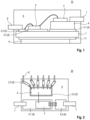
- Fig. 1 shows a cross-sectional side view on an example of a semiconductor package comprising a ceramic plate, a first conductive layer or film, a semiconductor transistor die, an electrical connector, a semiconductor logic die, and an encapsulant.
- a semiconductor package 10 comprises a semiconductor package 10, comprising a ceramic plate 1, a first conductive layer 2 disposed on the ceramic plate 1, the first conductive layer 2 comprising a first portion 2.1 and a second portion 2.2, a semiconductor transistor die 3 disposed above the first portion 2.1 of the first conductive layer 2, an electrical connector 4 disposed between the semiconductor transistor die 3 and the first portion 2.1 of the first conductive layer 2, a semiconductor logic die 5 disposed on the second portion 2.2 of the first conductive layer 2, and an encapsulant 6 covering at least in part the ceramic plate 1, the first conductive layer 2, the semiconductor transistor die 3 and the semiconductor logic die 5.
- the ceramic plate 1 is optionally disposed on a metallic substrate 9 which can be made of copper, aluminum or any composite of those metals.
- a thickness of the metallic substrate 9 can be in a range from 200 ⁇ m to 500 ⁇ m.
- a second conductive layer 11 can be disposed between the ceramic plate 1 and the metallic substrate 9. The second conductive layer 11 may have the same or similar properties as the first conductive layer 2.
- Fig. 1 Also shown in the embodiment of Fig. 1 are two bond wires, one being connected between a contact pad of the logic semiconductor die 5 and a gate pad of the power semiconductor die 3, and the other one being connected between another contact pad of the logic semiconductor die 5 and one of a plurality of third portions 2.3 of the first conductive layer 2.
- first external pins 7 connected with the semiconductor transistor die 3, and one of second external pins 8 connected with the logic semiconductor die 5.
- the first external pins 7 are connected with different portions of the electrical conductor 4, and the second external pins are connected with the third portions 2.3 of the first conductive layer 2.
- the semiconductor transistor die 3 can in particular be a power semiconductor transistor die 3.
- the term "power semiconductor transistor die” may refer to a semiconductor die providing at least one of high voltage blocking or high current-carrying capabilities.
- a power semiconductor die may be configured for high currents having a maximum current value of a few Amperes, such as e.g. 10 A, or a maximum current value of up to or exceeding 100 A.
- voltages associated with such current values may have values of a few Volts to a few tens or hundreds or even thousands of Volts.
- semiconductor dies 3 as described herein may be manufactured from an elemental semiconductor material (e.g. Si) or from a wide band gap semiconductor material or a compound semiconductor material (e.g. SiC, GaN, SiGe, GaAs) .
- an elemental semiconductor material e.g. Si
- a wide band gap semiconductor material e.g. SiC, GaN, SiGe, GaAs
- the ceramic plate 1 comprises one of Al 2 O 3 , AlN, Si 3 N 4 , or zirconia toughened alumina (ZTA), BeO, SiC, AlON, ZrO, or any other ceramic according to DIN V ENV 12212.
- ZTA zirconia toughened alumina
- the ceramic plate 1 comprises a thickness greater than 500 ⁇ m or greater than 600 ⁇ m or greater than 635 ⁇ m.
- the first conductive layer 2 comprises an International Annealed Copper Standard (IACS) >30%.
- IACS is an empirically derived standard value for the electrical conductivity of commercially available copper .
- the first conductive layer 2 comprises a copper basis with a share of >50%.
- the first conductive layer 2 is primarily a thick film paste and may comprise copper as a metal and optionally Bi 2 O 3 .
- the thick-film paste of the first conductive layer 2 comprises preferably 40 to 92 wt.-% copper, more preferably 40 to less than 92 wt.-% copper, more preferably 70 to less than 92 wt.-% copper, most preferably 75 to 90 wt.-% copper, each based on the total weight of the thick-film paste. Furthermore the thick-film paste comprises preferably 0 to 50 wt.-% Bi 2 O 3 , more preferably 1 to 20 wt.-% Bi 2 O 3 , most preferably 2 to 15 wt.-% Bi 2 O 3 , each based on the total weight of the thick-film paste.
- the copper particles used in the thick-film paste of the first conductive layer 2 have a median diameter (d 50 ) preferably of between 0.1 to 20 ⁇ m, more preferably of between 1 and 10 ⁇ m, most preferably of between 2 and 7 ⁇ m.
- the Bi 2 O 3 particles used optionally in the thick-film paste have a median diameter (d 50 ) preferably of less than 100 ⁇ m, more preferably of less than 20 ⁇ m, most preferably of less than 10 ⁇ m.
- the metal-containing thick-film paste of the first conductive layer 2 may comprise copper and a glass component.
- the amount of copper in the thick-film paste in case of a simultaneous use of a glass component might be as defined above, i.e. preferably in an amount of from 40 to 92 wt.-%, more preferably 40 to less than 92 wt.-% copper, more preferably in an amount of from 70 to less than 92 wt.-% copper, most preferably in an amount of from 75 to 90 wt.-% copper, each based on the total weight of the thick-film paste.
- the thick-film paste comprises preferably of from 0 to 50 wt.-%, more preferably 1 to 20 wt.-%, most preferably 2 to 15 wt.-%, of the glass component, each based on the total weight of the thick-film paste.
- the copper particles may have the same median diameter (d 50 ) as already mentioned above, i . e . preferably of between 0.1 to 20 ⁇ m, more preferably of between 1 and 10 ⁇ m, most preferably of between 2 and 7 ⁇ m.
- the glass component particles may have a median diameter (d 50 ) of less than 100 ⁇ m, more preferably less than 20 ⁇ m, most preferably less than 10 ⁇ m.
- the metal-containing thick-film paste may comprise - besides the glass component and Bi 2 O 3 - further components, selected from the group consisting of PbO, TeO2, Bi 2 O 3 , ZnO, B 2 O 3 , Al 2 O 3 , TiO 2 , CaO, K 2 O, MgO, Na 2 O, ZrO 2 , and Li 2 O.
- the amount of copper oxide in the thick-film paste of the first conductive layer 2 is less than 2 wt.-%, more preferably less than 1.9 wt.-%, more preferably less than 1.8 wt.-%, more preferably less than 1.5 wt.-%.
- first conductive layer 2 may be comprised out of commonly known active metal brazing alloys, e.g. Ag66Cu29.5Ti1.5.
- the layer thickness of the first conductive layer 2 is preferably of from 5 to 150 ⁇ m, more preferably of from 20 to 125 ⁇ m, most preferably of from 30 to 100 ⁇ m.
- the electrical connector 4 comprises an International Annealed Copper Standard >70%. According to an example thereof, the electrical connector 4 comprises one of OF-Copper or tough pitch copper (TPC).
- TPC tough pitch copper
- the electrical connector 4 comprises a thickness greater than 125 ⁇ m or greater than 300 ⁇ m.
- the encapsulant 6 may be comprised of a conventional mold compound like, for example, a resin material, in particular an epoxy resin material. Moreover, the encapsulant 6 can be made of a thermally conductive material to allow efficient heat dissipation to external application heat sinks.
- the material of the encapsulant 15 can, in particular, comprise a resin like an epoxy resin material filled with particles like, for example, SiO or other ceramic particles, or thermally conductive particles like, for examples, Al 2 O 3 , BN, AlN, Si 3 N 4 , diamond, or any other thermally conductive particles.
- two or more semiconductor transistor dies may be provided in the semiconductor package, which transistor dies may be connected to a driving logic die in the same way as the semiconductor die 3.
- the power semiconductor dies may particularly be used in half bridge configurations and/or boost configurations, such as e.g. buck-boost-converters or boost converters.
- the configurations may be used for industrial grade products applied in one or more of integrated servo motor inverters or PFC (Power Factor Correction) Boost stages, for example.
- Addressed applications may include automotive applications, industrial drive applications, EV (Electric Vehicle) charging, etc.
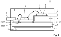
- Fig. 2 shows a down view on an example of a semiconductor package showing further details like external leads and their electrical connections to the semiconductor dies.
- FIG. 2 depicts a semiconductor device package 20 which is similar to the semiconductor device package 10 of Fig. 1 so that most of the reference signs of Fig. 1 were adopted and with regard to the function of the corresponding elements, reference is made to the above description.
- the semiconductor package 20 shows a plurality of second external pins 8 which are connected with the logic semiconductor die 5.
- the semiconductor package 20 furthermore shows a plurality of third portions 2.3 of the first conductive layer 2 and a particular arrangement of these third portions 2.3.
- the logic semiconductor die 5 has a plurality of contact pads on its upper surface. Each one of the third portions 2.3 of the first conductive layer 2 is connected at its outer end to one of the second external pins 8 and connected at its inner end to one of the contact pads of the logic semiconductor die 5 by means of a bonding wire.
- a width of each one of the third portions 2.3 of the first conductive layer 2 can be below 500 ⁇ m or below 250 ⁇ m and a pitch between adjacent third portions 2.3 can be below 1 mm or below 500 ⁇ m.
- the electrical conductor 4 comprises two portions 4.1 and 4.2.
- the semiconductor transistor die 3 is attached to an upper surface of a first portion 4.1 of the electrical conductor 4 which first portion 4.1 is connected by bond wires or clips to a second portion 4.2 of the electrical conductor 4.
- One of the first external leads 7 is connected to the first portion 4.1, and another one of the first external leads 7 is connected with the second portion 4.2.
- Fig. 3 shows a cross-sectional side view on an example of a semiconductor package similar to the one of Fig. 1 with an additional plated layer on the first conductive layer and the electrical connector.
- FIG. 3 depicts a semiconductor device package 20 which is similar to the semiconductor device package 10 of Fig. 1 so that most of the reference signs of Fig. 1 were adopted and with regard to the function of the corresponding elements, reference is made to the above description.
- the semiconductor package 20 of Fig. 3 comprises an additional layer 12 of electroless plating or an electroplating of copper, nickel, gold, silver or any layer stack thereof to provide an improved electrical conductivity and/or compatibility to common interconnect technologies.
- a further such layer can also be applied to the metallic substrate 9.
- Example 1 is a semiconductor package, comprising a ceramic plate, a first conductive layer disposed on the ceramic plate, the first conductive layer comprising a first portion and a second portion, a semiconductor transistor die disposed above the first portion of the first conductive layer, an electrical connector disposed between the semiconductor transistor die and the first portion of the first conductive layer, a semiconductor logic die disposed on the second portion of the first conductive layer, and an encapsulant covering at least in part the ceramic plate, the first conductive layer, the semiconductor transistor die and the semiconductor logic die.
- Example 2 is the semiconductor package according to Example 1, wherein the ceramic plate comprises one of Al2O3, AlN, Si3N4, or zirconia toughened alumina, BeO, SiC, or any other ceramic according to DIN V ENV 12212.
- Example 3 is the semiconductor package according to Example 1 or 2, wherein the ceramic plate comprises a thickness greater than 500 ⁇ m or greater than 600 ⁇ m or greater than 635 ⁇ m.
- Example 4 is the semiconductor package according to any one of the preceding Examples, wherein the first conductive layer comprises an electrical conductivity of >30% according to the International Annealed Copper Standard.
- Example 5 is the semiconductor package according to Example 4, wherein the first conductive layer comprises a copper basis with a share of >50%.
- Example 6 is the semiconductor package according to any one of the preceding Examples, wherein a thickness of the first conductive layer is in a range from 5 to 150 ⁇ m, or from 20 to 125 ⁇ m, or from 30 to 100 ⁇ m.
- Example 7 is the semiconductor package according to any one of the preceding Examples, wherein the electrical connector comprises an electrical conductivity of >70% according to the International Annealed Copper Standard.
- Example 8 is the semiconductor package according to any one of the preceding Examples, wherein the electrical connector comprises one of OF-Copper or tough pitch copper.
- Example 9 is the semiconductor package according to any one of the preceding Examples, wherein the electrical connector comprises a thickness greater than 125 ⁇ m or greater than 300 ⁇ m.
- Example 10 is the semiconductor package according to any one of the preceding Examples, further comprising a plurality of pins, wherein first pins of the plurality of pins are connected with the semiconductor transistor die, and second pins of the plurality of pins are connected with the semiconductor logic die.
- Example 11 is the semiconductor package according to any one of the preceding Examples, wherein the first conductive layer comprises a plurality of third portions disposed on the ceramic plate, each one of the third portions connected with one of the second pins.
- Example 12 is the semiconductor package according to any one of the preceding Examples, wherein the ceramic plate is disposed on a metallic substrate.
- Example 13 is the semiconductor package according to Example 12, wherein a second conductive layer is disposed between the ceramic plate and the metallic substrate.
- Example 14 is the semiconductor package according to any one of the preceding Examples, further comprising a further conductive layer covering the first conductive layer and the electrical connector.
- Example 15 is the semiconductor package according to Example 14, wherein the further conductive layer is a plated layer.
- Example 16 is the semiconductor package according to Example 15, wherein the plated layer is an electroless plating of copper, nickel, gold, silver or any layer stack thereof.
- Example 17 is the semiconductor package according to any one of the preceding Examples, wherein the semiconductor transistor die is a power semiconductor transistor die.
Landscapes
- Lead Frames For Integrated Circuits (AREA)
- Engineering & Computer Science (AREA)
- Cooling Or The Like Of Semiconductors Or Solid State Devices (AREA)
- Microelectronics & Electronic Packaging (AREA)
- Chemical & Material Sciences (AREA)
- Ceramic Engineering (AREA)
Priority Applications (3)
| Application Number | Priority Date | Filing Date | Title |
|---|---|---|---|
| EP22171175.7A EP4273928A1 (de) | 2022-05-02 | 2022-05-02 | Halbleitergehäuse mit leistung und logik auf einer einzelnen keramikplate |
| CN202310467894.4A CN116995037A (zh) | 2022-05-02 | 2023-04-27 | 一种包含组合功率和逻辑衬底的半导体封装 |
| US18/141,497 US20230352462A1 (en) | 2022-05-02 | 2023-05-01 | Semiconductor Package Comprising a Combined Power and Logic Substrate |
Applications Claiming Priority (1)
| Application Number | Priority Date | Filing Date | Title |
|---|---|---|---|
| EP22171175.7A EP4273928A1 (de) | 2022-05-02 | 2022-05-02 | Halbleitergehäuse mit leistung und logik auf einer einzelnen keramikplate |
Publications (1)
| Publication Number | Publication Date |
|---|---|
| EP4273928A1 true EP4273928A1 (de) | 2023-11-08 |
Family
ID=81580774
Family Applications (1)
| Application Number | Title | Priority Date | Filing Date |
|---|---|---|---|
| EP22171175.7A Pending EP4273928A1 (de) | 2022-05-02 | 2022-05-02 | Halbleitergehäuse mit leistung und logik auf einer einzelnen keramikplate |
Country Status (3)
| Country | Link |
|---|---|
| US (1) | US20230352462A1 (de) |
| EP (1) | EP4273928A1 (de) |
| CN (1) | CN116995037A (de) |
Citations (3)
| Publication number | Priority date | Publication date | Assignee | Title |
|---|---|---|---|---|
| US20080106875A1 (en) * | 2004-02-24 | 2008-05-08 | Yusuke Igarashi | Circuit Device And Method Of Manufacturing The Same |
| US20120134115A1 (en) * | 2009-07-02 | 2012-05-31 | Curamik Electronics Gmbh | Electronic device |
| US20150085454A1 (en) * | 2013-09-23 | 2015-03-26 | Delta Electronics (Shanghai) Co., Ltd. | Power module |
Family Cites Families (9)
| Publication number | Priority date | Publication date | Assignee | Title |
|---|---|---|---|---|
| DE10149774A1 (de) * | 2001-10-09 | 2003-04-24 | Bosch Gmbh Robert | Verfahren zum Verpacken von elektronischen Baugruppen und Mehrfachchipverpackung |
| DE102005062783A1 (de) * | 2005-12-28 | 2007-07-05 | Robert Bosch Gmbh | Elektronikmodul sowie Verfahren zur Herstellung eines solchen |
| US8872326B2 (en) * | 2012-08-29 | 2014-10-28 | Taiwan Semiconductor Manufacturing Company, Ltd. | Three dimensional (3D) fan-out packaging mechanisms |
| US20140197527A1 (en) * | 2013-01-16 | 2014-07-17 | Infineon Technologies Ag | Chip arrangement and a method for manufacturing a chip arrangement |
| US20160329312A1 (en) * | 2015-05-05 | 2016-11-10 | Sean M. O'Mullan | Semiconductor chip with offloaded logic |
| JP7071499B2 (ja) * | 2018-06-20 | 2022-05-19 | ローム株式会社 | 半導体装置 |
| US20200098727A1 (en) * | 2018-09-25 | 2020-03-26 | Debendra Mallik | Stacked wire-bond dice attached by pillars or bumps above a flip-chip die on a semiconductor package substrate |
| DE102019104010B4 (de) * | 2019-02-18 | 2025-08-28 | Infineon Technologies Austria Ag | Elektronisches modul mit verbesserter wärmeabfuhr und dessen herstellung |
| US12604732B2 (en) * | 2021-02-26 | 2026-04-14 | Infineon Technologies Austria Ag | Power electronics carrier |
-
2022
- 2022-05-02 EP EP22171175.7A patent/EP4273928A1/de active Pending
-
2023
- 2023-04-27 CN CN202310467894.4A patent/CN116995037A/zh active Pending
- 2023-05-01 US US18/141,497 patent/US20230352462A1/en active Pending
Patent Citations (3)
| Publication number | Priority date | Publication date | Assignee | Title |
|---|---|---|---|---|
| US20080106875A1 (en) * | 2004-02-24 | 2008-05-08 | Yusuke Igarashi | Circuit Device And Method Of Manufacturing The Same |
| US20120134115A1 (en) * | 2009-07-02 | 2012-05-31 | Curamik Electronics Gmbh | Electronic device |
| US20150085454A1 (en) * | 2013-09-23 | 2015-03-26 | Delta Electronics (Shanghai) Co., Ltd. | Power module |
Also Published As
| Publication number | Publication date |
|---|---|
| US20230352462A1 (en) | 2023-11-02 |
| CN116995037A (zh) | 2023-11-03 |
Similar Documents
| Publication | Publication Date | Title |
|---|---|---|
| US11532538B2 (en) | Component structure, power module and power module assembly structure | |
| US10483216B2 (en) | Power module and fabrication method for the same | |
| US9659912B2 (en) | Low-inductance circuit arrangement comprising load current collecting conductor track | |
| US8441128B2 (en) | Semiconductor arrangement | |
| US20220344310A1 (en) | Semiconductor module | |
| US8120153B1 (en) | High-temperature, wirebondless, injection-molded, ultra-compact hybrid power module | |
| EP2164100A2 (de) | Bleihaltiges Halbleiterleistungsmodul mit Direktbindung und doppelseitiger Kühlung | |
| US20230361009A1 (en) | Semiconductor package having an embedded electrical conductor connected between pins of a semiconductor die and a further device | |
| US20260053029A1 (en) | Semiconductor device | |
| WO2021130110A1 (en) | Power module with improved electrical and thermal characteristics | |
| US11973063B2 (en) | Semiconductor package with low parasitic connection to passive device | |
| EP4040472A1 (de) | Halbleiterbauelement und verfahren zur herstellung eines halbleiterbauelements | |
| CN108346587A (zh) | 芯片封装器件及封装方法 | |
| EP3739756A1 (de) | Kaskodenhalbleiterbauelement und verfahren zur herstellung | |
| EP4273928A1 (de) | Halbleitergehäuse mit leistung und logik auf einer einzelnen keramikplate | |
| EP3770962A1 (de) | Halbleitermodulanordnung | |
| JP7555486B2 (ja) | パワー半導体装置及び電力変換装置 | |
| CN114050134B (zh) | 半导体电路 | |
| EP4187595A1 (de) | Anschlusselement oder sammelschiene und leistungshalbleitermodulanordnung mit einem anschlusselement oder einer sammelschiene | |
| EP2722885B1 (de) | Oberflächenmontierbare Leistungskomponenten | |
| US20240304600A1 (en) | Chip-to-chip stacking by use of nickel tin metallization stacks and diffusion soldering | |
| US20240234267A1 (en) | Semiconductor device | |
| EP4261878A1 (de) | Mehrchipvorrichtung mit gaterumverteilungsstruktur | |
| US20250391805A1 (en) | Semiconductor device | |
| US20240222232A1 (en) | Semiconductor device |
Legal Events
| Date | Code | Title | Description |
|---|---|---|---|
| PUAI | Public reference made under article 153(3) epc to a published international application that has entered the european phase |
Free format text: ORIGINAL CODE: 0009012 |
|
| STAA | Information on the status of an ep patent application or granted ep patent |
Free format text: STATUS: THE APPLICATION HAS BEEN PUBLISHED |
|
| AK | Designated contracting states |
Kind code of ref document: A1 Designated state(s): AL AT BE BG CH CY CZ DE DK EE ES FI FR GB GR HR HU IE IS IT LI LT LU LV MC MK MT NL NO PL PT RO RS SE SI SK SM TR |
|
| STAA | Information on the status of an ep patent application or granted ep patent |
Free format text: STATUS: REQUEST FOR EXAMINATION WAS MADE |
|
| 17P | Request for examination filed |
Effective date: 20240430 |
|
| RBV | Designated contracting states (corrected) |
Designated state(s): AL AT BE BG CH CY CZ DE DK EE ES FI FR GB GR HR HU IE IS IT LI LT LU LV MC MK MT NL NO PL PT RO RS SE SI SK SM TR |