EP4274039A2 - Duplexer und zugehörige vorrichtungen für 5g/6g und nachfolgende protokolle und für mm-wellen- und terahertzanwendungen - Google Patents
Duplexer und zugehörige vorrichtungen für 5g/6g und nachfolgende protokolle und für mm-wellen- und terahertzanwendungen Download PDFInfo
- Publication number
- EP4274039A2 EP4274039A2 EP23181886.5A EP23181886A EP4274039A2 EP 4274039 A2 EP4274039 A2 EP 4274039A2 EP 23181886 A EP23181886 A EP 23181886A EP 4274039 A2 EP4274039 A2 EP 4274039A2
- Authority
- EP
- European Patent Office
- Prior art keywords
- duplexer
- shaped
- rectangular
- stub resonator
- stub
- Prior art date
- Legal status (The legal status is an assumption and is not a legal conclusion. Google has not performed a legal analysis and makes no representation as to the accuracy of the status listed.)
- Withdrawn
Links
- 238000004891 communication Methods 0.000 claims abstract description 30
- 238000010521 absorption reaction Methods 0.000 claims abstract description 20
- 230000004044 response Effects 0.000 claims description 74
- 229910052751 metal Inorganic materials 0.000 claims description 57
- 239000002184 metal Substances 0.000 claims description 57
- 238000005516 engineering process Methods 0.000 claims description 30
- 238000002955 isolation Methods 0.000 claims description 25
- 238000004519 manufacturing process Methods 0.000 claims description 10
- 229910001218 Gallium arsenide Inorganic materials 0.000 claims description 4
- 238000013461 design Methods 0.000 description 52
- 239000010410 layer Substances 0.000 description 51
- 238000010586 diagram Methods 0.000 description 41
- 230000005540 biological transmission Effects 0.000 description 19
- 239000000758 substrate Substances 0.000 description 18
- 230000009471 action Effects 0.000 description 12
- 238000000034 method Methods 0.000 description 11
- 230000000694 effects Effects 0.000 description 8
- 230000008901 benefit Effects 0.000 description 7
- 238000003780 insertion Methods 0.000 description 7
- 230000037431 insertion Effects 0.000 description 7
- 230000008878 coupling Effects 0.000 description 6
- 238000010168 coupling process Methods 0.000 description 6
- 238000005859 coupling reaction Methods 0.000 description 6
- 238000000862 absorption spectrum Methods 0.000 description 5
- 238000010897 surface acoustic wave method Methods 0.000 description 5
- 238000001914 filtration Methods 0.000 description 4
- 230000010354 integration Effects 0.000 description 4
- 230000005855 radiation Effects 0.000 description 4
- 238000004088 simulation Methods 0.000 description 4
- 230000003595 spectral effect Effects 0.000 description 4
- 238000002834 transmittance Methods 0.000 description 4
- 230000001149 cognitive effect Effects 0.000 description 3
- 230000007423 decrease Effects 0.000 description 3
- 238000009826 distribution Methods 0.000 description 3
- 239000000463 material Substances 0.000 description 3
- 230000007704 transition Effects 0.000 description 3
- VYPSYNLAJGMNEJ-UHFFFAOYSA-N Silicium dioxide Chemical compound O=[Si]=O VYPSYNLAJGMNEJ-UHFFFAOYSA-N 0.000 description 2
- 238000003491 array Methods 0.000 description 2
- 239000004020 conductor Substances 0.000 description 2
- 238000011161 development Methods 0.000 description 2
- 230000005684 electric field Effects 0.000 description 2
- 230000005281 excited state Effects 0.000 description 2
- 230000006870 function Effects 0.000 description 2
- 230000006872 improvement Effects 0.000 description 2
- 230000003278 mimic effect Effects 0.000 description 2
- 238000010295 mobile communication Methods 0.000 description 2
- 230000005404 monopole Effects 0.000 description 2
- 230000008569 process Effects 0.000 description 2
- 238000012545 processing Methods 0.000 description 2
- 239000000523 sample Substances 0.000 description 2
- 239000002356 single layer Substances 0.000 description 2
- WFKWXMTUELFFGS-UHFFFAOYSA-N tungsten Chemical compound [W] WFKWXMTUELFFGS-UHFFFAOYSA-N 0.000 description 2
- 229910052721 tungsten Inorganic materials 0.000 description 2
- 239000010937 tungsten Substances 0.000 description 2
- XUIMIQQOPSSXEZ-UHFFFAOYSA-N Silicon Chemical compound [Si] XUIMIQQOPSSXEZ-UHFFFAOYSA-N 0.000 description 1
- 210000001015 abdomen Anatomy 0.000 description 1
- 230000002411 adverse Effects 0.000 description 1
- 230000002776 aggregation Effects 0.000 description 1
- 238000004220 aggregation Methods 0.000 description 1
- 238000004458 analytical method Methods 0.000 description 1
- 230000003466 anti-cipated effect Effects 0.000 description 1
- 239000003990 capacitor Substances 0.000 description 1
- 230000008859 change Effects 0.000 description 1
- 229910052681 coesite Inorganic materials 0.000 description 1
- 210000001520 comb Anatomy 0.000 description 1
- 229910052906 cristobalite Inorganic materials 0.000 description 1
- 230000003247 decreasing effect Effects 0.000 description 1
- 230000001419 dependent effect Effects 0.000 description 1
- 230000001066 destructive effect Effects 0.000 description 1
- 230000002349 favourable effect Effects 0.000 description 1
- 239000011521 glass Substances 0.000 description 1
- 206010021198 ichthyosis Diseases 0.000 description 1
- 230000003993 interaction Effects 0.000 description 1
- 230000007246 mechanism Effects 0.000 description 1
- 150000002739 metals Chemical class 0.000 description 1
- 230000004048 modification Effects 0.000 description 1
- 238000012986 modification Methods 0.000 description 1
- 230000003287 optical effect Effects 0.000 description 1
- 238000005457 optimization Methods 0.000 description 1
- 230000037361 pathway Effects 0.000 description 1
- 230000001737 promoting effect Effects 0.000 description 1
- 230000009467 reduction Effects 0.000 description 1
- 238000000926 separation method Methods 0.000 description 1
- 229910052710 silicon Inorganic materials 0.000 description 1
- 239000010703 silicon Substances 0.000 description 1
- 239000000377 silicon dioxide Substances 0.000 description 1
- URWAJWIAIPFPJE-YFMIWBNJSA-N sisomycin Chemical compound O1C[C@@](O)(C)[C@H](NC)[C@@H](O)[C@H]1O[C@@H]1[C@@H](O)[C@H](O[C@@H]2[C@@H](CC=C(CN)O2)N)[C@@H](N)C[C@H]1N URWAJWIAIPFPJE-YFMIWBNJSA-N 0.000 description 1
- 238000001228 spectrum Methods 0.000 description 1
- 229910052682 stishovite Inorganic materials 0.000 description 1
- 230000001629 suppression Effects 0.000 description 1
- 229910052905 tridymite Inorganic materials 0.000 description 1
Images



























Classifications
-
- H—ELECTRICITY
- H01—ELECTRIC ELEMENTS
- H01P—WAVEGUIDES; RESONATORS, LINES, OR OTHER DEVICES OF THE WAVEGUIDE TYPE
- H01P7/00—Resonators of the waveguide type
- H01P7/08—Strip line resonators
- H01P7/082—Microstripline resonators
-
- H—ELECTRICITY
- H01—ELECTRIC ELEMENTS
- H01P—WAVEGUIDES; RESONATORS, LINES, OR OTHER DEVICES OF THE WAVEGUIDE TYPE
- H01P1/00—Auxiliary devices
- H01P1/20—Frequency-selective devices, e.g. filters
- H01P1/213—Frequency-selective devices, e.g. filters combining or separating two or more different frequencies
- H01P1/2135—Frequency-selective devices, e.g. filters combining or separating two or more different frequencies using strip line filters
-
- H—ELECTRICITY
- H01—ELECTRIC ELEMENTS
- H01P—WAVEGUIDES; RESONATORS, LINES, OR OTHER DEVICES OF THE WAVEGUIDE TYPE
- H01P1/00—Auxiliary devices
- H01P1/20—Frequency-selective devices, e.g. filters
- H01P1/201—Filters for transverse electromagnetic waves
- H01P1/203—Strip line filters
-
- H—ELECTRICITY
- H01—ELECTRIC ELEMENTS
- H01P—WAVEGUIDES; RESONATORS, LINES, OR OTHER DEVICES OF THE WAVEGUIDE TYPE
- H01P1/00—Auxiliary devices
- H01P1/20—Frequency-selective devices, e.g. filters
- H01P1/201—Filters for transverse electromagnetic waves
- H01P1/203—Strip line filters
- H01P1/20309—Strip line filters with dielectric resonator
-
- H—ELECTRICITY
- H01—ELECTRIC ELEMENTS
- H01P—WAVEGUIDES; RESONATORS, LINES, OR OTHER DEVICES OF THE WAVEGUIDE TYPE
- H01P1/00—Auxiliary devices
- H01P1/20—Frequency-selective devices, e.g. filters
- H01P1/201—Filters for transverse electromagnetic waves
- H01P1/203—Strip line filters
- H01P1/20327—Electromagnetic interstage coupling
- H01P1/20354—Non-comb or non-interdigital filters
- H01P1/20381—Special shape resonators
-
- H—ELECTRICITY
- H01—ELECTRIC ELEMENTS
- H01P—WAVEGUIDES; RESONATORS, LINES, OR OTHER DEVICES OF THE WAVEGUIDE TYPE
- H01P5/00—Coupling devices of the waveguide type
- H01P5/12—Coupling devices having more than two ports
-
- H—ELECTRICITY
- H01—ELECTRIC ELEMENTS
- H01P—WAVEGUIDES; RESONATORS, LINES, OR OTHER DEVICES OF THE WAVEGUIDE TYPE
- H01P7/00—Resonators of the waveguide type
- H01P7/10—Dielectric resonators
Definitions
- the inventions described herein relate to filters, duplexers, and related devices and systems for use in communication systems. Aspects of the inventions herein further relate to filters, duplexers, and related systems for use in 5G/6G and beyond communication protocols and systems, and mm- Wave and Terahertz (THz) communication systems.
- THz Terahertz
- 5G is a mobile communication system that supports multiple frequency bands and a multitude of modulation standards.
- 5G chipsets have several transverses and antenna.
- Active phased-array antennas APAAs
- MMIMO Massive MIMO
- SoC System-on-Chip
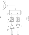
- Each RF front end is likely to contain some combination of components including the Power Amplifier (PA), Low Noise Amplifier (LNA), Switch, Phase Shifter (PS), Duplexers, and Variable Gain Amplifier (VGA) as shown in Figure 1 .
- PA Power Amplifier
- LNA Low Noise Amplifier
- PS Phase Shifter
- VGA Variable Gain Amplifier
- No single chip technology such as Si, GaAs or GaN, can provide the optimum workable solution with the anticipated specification for the above-mentioned RF components in 5G systems due to the required mm frequencies (28-56 GHz) and bandwidth in the GHz range. These frequencies will increase up to the range of 100 GHz to 1 THz (terahertz) and beyond for future 6G systems.
- TDD Time-Division Duplexing
- FDD Frequency-Division Duplexing
- the transmitter 112 and the receiver 114 operate simultaneously and share the same antenna 110.
- a duplexer 108 comprising of two selective filters: one filter that is centered at the transmission band (Tx) and the other filter that is centered at the reception band (Rx) to discriminate between the Tx and Rx signals.
- the antenna 110 operates at both bands and the duplexer 108 allows simultaneous transmit and receive communication with maximum isolation between Tx and Rx bands. Sharing a single antenna (SISO) or set of multiple antenna (MIMO) in a transmit and receive path reduces the size, weight and area of the transceiver system 100.
- SISO single antenna
- MIMO multiple antenna
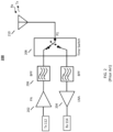
- TDD systems such as shown in Figure 2
- multiple signals are allowed to be transmitted on a single frequency band.
- the Tx and Rx operate at different time slots and feed the PA 202 and the LNA 204, respectively, at different time instants.
- the emergence of beamforming MIMO systems has drawn an immense interest in a fully integrated SoC solution with a large number of on-chip antennas along with the associated Tx and Rx RF chains.
- FDD type architectures are more favorable for beamforming MIMO systems compared to TDD. Therefore, the duplexer, being an essential part of the RF chain, must be integrated on the single CMOS chip containing all of the other RF chain components.
- a Duplexer-on-Chip (DoC) along with an Antenna-on-Chip (AoC) may be a viable solution for the design and development of fully integrated, low-cost, power-efficient mm-wave future 5G/6G transceivers.
- duplexers consist of two passband filters that are tuned at different frequencies while providing good isolation between the ports of the filters. They are selective components used to isolate or combine signals having different central frequencies and are essential components of FDD communication systems including, but not limited to, mobile telephony, radio transmission, broadband wireless communications, and satellite communication systems.
- the duplexer is a 3-port filtering device that must provide good isolation between the transmitter and the receiver while maintaining a low insertion loss (by the duplexer itself).
- Duplexers typically consist of two-channel filters, and a common point is used to combine the two filters to form the multiport network as shown in the duplexer 304 of Figure 3 .
- duplexer 304 provides a mechanism for a transmitter 310 and a receiver 312 to share a common antenna 302 simultaneously.
- the antenna 302 operates at both bands and the duplexer 304 allows simultaneous communication with maximum isolation between the Tx and Rx bands.
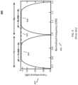
- duplexing gap 402 is the duplexer separation between transmit band 404 and receive band 406. There is no overlapping between bands 404 and 406 which means a good isolation is achieved by duplexer 304.
- Table 1 Summary of various types of passive duplexers Waveguides Duplexers Dielectric Resonators Duplexers Planar Duplexers Quasi-Planar Duplexers SIW Duplexers HTS Size Large Large Small Large Moderate Small EM Simulation 3D 3D 2D & 3D 3D 3D 2D & 3D Ease of Integration on a Single Chip Difficult Difficult Excellent Moderate Moderate Excellent Quality factor Very High Very High Low High Low Power Handling High High Low High Low Low Low
- the two main classes of duplexers are active and passive.
- the active duplexers have a small on-chip area and also provide the necessary gain.
- the transistors are fabricated on the substrate, the routing of a wideband mm-wave signal from the antenna to the substrate through tungsten (W) vias and the low transistor-to-transistor isolation in the substrate pose a significant technical challenge. Therefore, the active class of duplexers is generally not deemed suitable for mm-wave solutions due to low suppression of the undesired frequency band.
- the PA signal leaks through the substrate and drives the LNA in the non-linear region.
- the passive class of duplexers provides better isolation since they do not suffer from the substrate coupling problem. Moreover, they typically do not have any biasing requirements and can be fabricated using the single or multiple metal layers available for interconnect in the CMOS technology.
- the passive class of duplexers can be implemented using a variety of different technologies as listed above in Table I. These types of passive class duplexers have their own merits and demerits in terms of size, Q-factor, cost, insertion loss, isolation, ease of integration, and power handling capacity. All passive class duplexer types are not necessarily suitable for on-chip implementation due to the planar nature of the existing CMOS process, the small feature size, and the types of the metals used for on-chip interconnect.
- Waveguide-based duplexers are suitable for high power applications; however, their large structure size renders them unsuitable for on-chip integration.
- Some non-traditional duplexer designs use power limiters, couplers, and phase shifters to achieve the duplexing action.
- the limiter blocks the signal and establishes the connection between transmitter, antenna and vice versa.
- Microstrip based duplexer designs are simple, easy to fabricate and their ability to integrate with planar structures makes them potential candidates for on-chip duplexer design. These designs have shown good performance at low frequencies, but at mm-wave, they exhibit high radiation losses which render them a poor choice for 5G/6G applications. The emerging techniques to mitigate the radiation and substrate losses can make these designs an attractive choice for future 5G/6G applications. These planar duplexers are considered to be the most suitable type of duplexers for on-chip fabrication. A 3-port planar passive tunable duplexer was proposed by Psychogiou et al. and its structure was designed for low frequency bands. The tuneability was achieved with the help of capacitors. In 5G/6G systems, the selectivity of the duplexer filter is a major challenge.
- Chinig et al. proposed an open loop microstrip based duplexer and triplexer.
- the low-quality factor of such microstrip technology is considered a bottleneck and, so far, several techniques have been proposed to mitigate this shortcoming.
- the microstrips were used as feed lines and duplexing and triplexing actions were achieved by cascading different bandpass filters, tuned at different frequencies. The design offers good isolation and low insertion loss which shows that these types of filters with open loops may have the potential for use in duplexers for mm-wave applications.
- the passive Surface Acoustic Wave (SAW) filter duplexer was proposed by T. Matsuda, et al.
- the SAW filter duplexer has high losses, and it was mainly designed for low-frequency communication systems like the AMPS-CDMA system.
- a miniature bulk acoustic wave (BAW) duplexer for on-chip solutions has been proposed but its structure was bulky and it was also designed for low-frequency applications.
- a CMOS technology-based nonreciprocal wideband transmission line duplexer was proposed by Yang.
- An isolator at an extremely high frequency was proposed by Wang et al. which uses unidirectional split-ring resonators.
- An mm-wave microstrip duplexer using elliptical open-loop ring resonators for 5G applications was proposed by Haraz et al., wherein a set of two elliptical resonating filters were used to achieve the duplexing behavior.
- a stub-tuned microstrip bandpass filter for mm-Wave duplexer is proposed by Hong et al., in which a pair of parallel-coupled microstrip lines of 510 mils (12.9 mm) and 452 mils (11.4 mm) is used. This particular design is proposed for 5G applications; however, the large dimensions make them unsuitable for on-chip integration.
- a waveguide duplexer is described in US Patent Publication No. US20070139135A1 (Ammar, et al. ). Such waveguide-based structures are good for high power handling capacity, but they are bulky and difficult to integrate with planar structures.
- a T-shaped microstrip duplexer for low frequencies 1-3 GHz is shown in the Patent EA021016B1 (Belyaev et al. ) wherein the filtering effect at different frequencies is achieved by different lengths of the microstrip.
- Duplexer design using through-glass via technology is described in the U.S. Patent No. 9,203,373 ( Zuo ) wherein the substrate has a number of through vias and set of traces that behave as an inductor.
- the size of all such duplexers is large and most of these duplexers are either designed for low frequencies or exhibit attenuation in their frequency response.
- existing technology does not provide suitable designs for a small size, low power, and high isolation on-chip duplexer for a 5G/6G System.
- the expected number of antennas ranges from 4 to 512 on the single chip.
- the same number of duplexers are also needed on the same single CMOS chip.
- CMOS chip size exceeds the order of size more than 30 ⁇ 30 mm 2 , then the matching and reliability issues become dominant. As a result, the yield of the SoC will be reduced. Therefore, innovative and out of the box designs are required for 5G/6G duplexer technology.
- a ring resonator based T-shaped duplexer for use in communication systems, the T-shaped duplexer comprising a T-shaped microstrip duplexer body having a first rectangular-shaped body section and a second rectangular-shaped body section that extends from the first-rectangular shaped section in a perpendicular position relative to the first rectangular-shaped section, three connection ports including a first connection port disposed at an open end of the second rectangular-shaped body section, a second connection port disposed at one end of the first rectangular-shaped body section, and a third connection port disposed at another end of the first rectangular-shaped body section, and two bandpass filters, each bandpass filter comprising a ring resonator structure having a circular shape, an outer edge of the ring resonator structure being connected to the first rectangular-shaped body section of the T-shaped microstrip duplexer body, wherein each of the two bandpass filters creates an Electromagnetically Induced Transparency (EIT) window within a frequency absorption
- EIT Electro
- a ring resonator based bandpass filter device for use in communication systems, the bandpass filter device comprising a microstrip structure having a rectangular shaped body and having a first port provided at one end of the rectangular shaped body and a second port provided at a second end of the rectangular shaped body, and a ring resonator structure having a circular shape, an outer edge of the ring resonator structure being connected to the rectangular shaped body of the microstrip structure, wherein the ring resonator structure creates an Electromagnetically Induced Transparency (EIT) window within a frequency absorption region of the bandpass filter device to allow a signal to pass at a pre-tuned frequency band.
- EIT Electromagnetically Induced Transparency
- a stub resonator based T-shaped duplexer for use in communication systems, the T-shaped duplexer comprising a T-shaped microstrip duplexer body having a first rectangular-shaped body section and a second rectangular-shaped body section that extends from the first-rectangular shaped section in a perpendicular position relative to the first rectangular-shaped section, three connection ports including a first connection port disposed at an open end of the second rectangular-shaped body section, a second connection port disposed at one end of the first rectangular-shaped body section, and a third connection port disposed at another end of the first rectangular-shaped body section, and two bandpass filters connected to the first rectangular-shaped body section of the T-shaped microstrip duplexer body, each bandpass filter comprising a rectangular microstrip structure, a first rectangular stub resonator structure extending from the rectangular microstrip structure in a perpendicular direction relative to the microstrip structure, and a second rectangular stub resonator structure
- a stub resonator based bandpass filter device for use in communication systems, the bandpass filter device comprising a microstrip structure having a rectangular shaped body and having a first port provided at one end of the rectangular shaped body and a second port provided at a second end of the rectangular shaped body, a first stub resonator structure having a rectangular shape and extending from the rectangular shaped body of the microstrip structure in a perpendicular direction relative to the rectangular shaped body of the microstrip structure, and a second stub resonator structure having a rectangular shape and extending from the rectangular shaped body of the microstrip structure in a perpendicular direction relative to the rectangular shaped body of the microstrip structure, the second stub resonator structure being in a parallel position relative to the first stub resonator structure and being separated from the first stub resonator structure by a gap distance, wherein the first stub resonator structure and the second stub
- Microstrip based filters are known for their planar structure and their ability to integrate with other components.
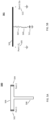
- the open-circuit microstrip stub 508 in the microstrip line 506 shown in Figure 5A behaves like a resonator and resonates at a particular resonance frequency that depends on the dimensions and permittivity of the host material.
- the microstrip stub behaves like RLC series circuit connected between the ground and a microstrip line as shown in the schematic depiction of Figure 5B .
- the signal wave at port-t 502 gets absorbed at open circuit stub 508 and due to its strong absorption, a low amplitude signal is received at port-2 504.
- the microstrip line 506 transmits as shown in the frequency response graph of Figure 6 and a strong absorption 608 at the resonance frequency is observed.
- Figure 5B shows an equivalent series RLC schematic implementation of the transmission line resonator that was depicted in Figure 5A .
- the transmission response can be obtained by applying the microwave Kirchhoff's current equation (Equation 1 below) to the transmission line and stub combination of Figure 5 .
- S 21 2 Z o 2 AZ o + A 2 Z o 2 B + B ⁇ Z o 2 B
- duplexer technology to make duplexers suitable for 5G/6G mm-wave and Terahertz (THz) applications.
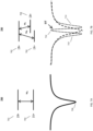
- a transparency window within the Lorentz absorption region can be created because of an Electromagnetically Induced Transparency (EIT) response of the transmission line of the duplexer as shown in Figures 7A and 7B .
- EIT Electromagnetically Induced Transparency
- the concept of EIT is a well-known quantum phenomenon.
- the resonators tuned at different frequencies can be used to make a bandpass filter.
- the class of resonance exhibited by such type of structures is called Electromagnetically Induced Transparency (EIT).
- EIT Electromagnetically Induced Transparency
- a transparency window within the Lorentz absorption region 706 is provided and can also be produced as EIT region 712 as shown in Figure 7B .
- the wave interference that leads to EIT requires at least a three-level atomic structure so that two transition pathways connecting the ground to the excited state are available.
- A-type atomic structure of Figure 7B in which two allowed dipole transitions are given by 704
- a probe laser is applied to the resonance of the state transition
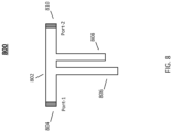
- a double stub bandpass microwave filter 800 is shown in Fig. 8 .
- the stubs 806 and 808 extending from the microstrip 802 behaves as an LC filter and allows the signal to pass at a particular pre-tuned frequency band.
- the opposite ends of microstrip 802 includes Port 1 804 and Port 2 810, respectively.
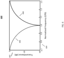
- a frequency response graph 900 for the filter of Figure 8 is provided in Figure 9 in which it can be seen that the filter stops the signal at stopbands 904 and 912 and allows the desired signal to pass at passband 910.
- Such type of filters can be fabricated using traditional CMOS technology.
- the out-of-band rejection of the EIT filter is poor and limits its use where the number of channels is large like in Massive-MIMO systems.
- a special type of EIT called Fano with an asymmetric profile can be used to obtain high selectivity.
- Fano with an asymmetric profile
- Such type of resonance is used in photonics and optical sensor design to achieve high selectivity.
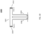
- the double stub EIT filter of Figure 8 is modified as filter 1000 in Figure 10 in such a way that both stubs 1006 and 1008 have the same length and therefore resonate at the same frequency. Consequently, a high-quality factor (Q) response is produced.
- a frequency response graph 1100 for filter 1000 is shown in Figure 11 in which it can be seen that a normalized Fano resonance with high quality factor (Q) of 700 is achieved.
- Such type of high Q filters can be used to design duplexers for massive MIMO applications for 5G/6G systems and beyond.
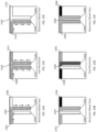
- Figures 12A through 12F show the nodal currents at three spectral resonance points for a filter having different stub lengths. When stub lengths are different, they change the surface distributions of current. As seen in Figures 12A and 12B , when the length of conducting paths 1202, 1204, 1222 become a quarter wavelength, just like the series resonant circuit, the phase of the resonant branch remains equal to that of the input port, and the dominant current flows back to the input port thus creating a transmission dip. Similarly, as shown in Figures 12E and 12F when the length of the first stub 1228 is a quarter wavelength, a perfect resonance dip with zero transmission is observed because there is no alternate path other than the virtual short circuit at point 1214.
- a second arrangement is to make the stub lengths of the filter equal in length and this results in a Fano based design as shown in Figures 13A to 13F .
- Fano when the length of conducting path 1302, 1304, 1322 becomes close to a quarter wave length, just like the series resonant circuit, the phase of the resonant branch remains equal to that of the input port, and the dominant current flows back to the input port creating a transmission dip.
- Figures 13E and 13F when the first stub 1314 attains the length of quarter wavelength, all the currents return to the input port through the conducting path 1314, 1328 and the output is completely cut-off.
- the stubs can be replaced by lumped components, as shown in Figure 5B for the two-stub configuration.
- the transmittance spectra, such as shown in Figure 9 can be fitted with the RLC resonator transmission response to subsequently extract the RLC lumped element values.
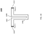
- a third arrangement is also possible that results in a classical Lorentzian resonance as shown in filter 1400 of Figure 14 .
- Both ends of the microstrip stubs are joined at end 1406 in such a way that they make a U-shaped structure and as a result a gap 1408 is created in microstrip 1402.
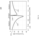
- the phenomenon of resonance for such a filter 1400 changes from EIT to Lorentz as shown in the frequency response graph 1500 of Figure 15 .
- the response offers good stopbands 1506 and 1510.
- the peak 1508 is not as sharp as compared to 1108 of Figure 11 .
- the Q factor of Lorentz-based resonance is relatively small as compare to Fano resonance.
- Figure 16 shows a simple microstrip structure 1604 with a length L 1 .
- the advantage of a Lorentz structure over Fano and EIT structures is that it can be bent into a spiral shape 1610 as shown in Figure 16 .
- the spiral-shaped structure 1610 reduces the size of the resonator depending on the number of turns. For N number of turns, the size is reduced by approximately N/4.
- the quality factor of all three resonances can be controlled by making minor changes in the geometry of the stubs, such as changes in length, width, or spacing between the stubs.
- EIT offers the maximum bandwidth.
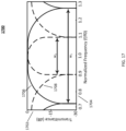
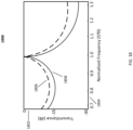
- the bandwidth of an EIT filter can be controlled by changing the difference in the lengths of the open-circuit stubs, such as stubs 806 and 808 of Figure 8 . If the difference in the lengths is large, the absorption frequency of both stubs will be far from each other and hence response with larger bandwidth will be achieved as shown in the frequency response graph 1700 of Figure 17 .
- the bandwidth of the curve 1706 is much larger than the bandwidth of the curve 1708.
- the bandwidth can be controlled by just changing the length of the open stubs, such as stubs 806 and 808 of Figure 8 .
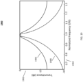
- the bandwidth of the Fano-filters can be changed by changing the distance w between the stubs, such as stubs 1006 and 1008 of Figure 10 .
- the frequency response graph 1700 for such a filter is shown in Figure 18 in which it can be seen that the bandwidth of 1808 is much smaller than the bandwidth of 1806 which means that the selectivity of Fano-based resonating filters is highly dependent on the distance w between the open stubs in the microstrip. This happens because of the increase in the intensity of the electric field originating from the stubs' side walls facing each other. These electric field lines become concentrated and the interaction becomes more pronounced with the decrease in the distance between the open-circuit stubs.
- the bandwidth of the Lorentzian filters is also controllable, but contrary to the EIT and Fano filters, the bandwidth is controlled in the Lorentzian filters by the width of the microstrip line.
- ⁇ c is the attenuation coefficient due to conductor losses
- ⁇ d is the attenuation coefficient due to dielectric losses.
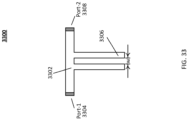
- T-shape duplexer 2000 in Figure 20 in which two bandpass filters BPFs 2020 and 2024 are used to achieve the duplexing action. Both filters 2020 and 2024 are tuned to resonate at different frequencies so that band selection and good isolation can be achieved.
- One port 2022 (Port-1) of the duplexer 2000 will be attached to the antenna and other ports 2012 (Port-2) and 2014 (Port-3) will be attached to the transmitter and the receiver, respectively.
- the general behavior of the T-shape duplexer 2000 is shown in the frequency response graph 2100 of Figure 21 .
- the high isolation between both BPFs 2020 and 2024 is a key requirement in achieving the duplexing action.
- the T-shape of the duplexer not only reduces the overall size but also helps to implement the duplexer on the single layer of a CMOS IC stack making it a planer structure.
- the duplexer divides the input signal 2026 into two signals, one at a high frequency 2006 and the other at a low frequency 2002 due to the BPF 2020 and 2024.
- the duplexer design is suitable for 5G/6G and THz applications as it can be easily manufactured using standard CMOS IC technology.
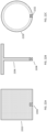
- FIGS 22A to 22C The top views of an IC containing different on-chip antennas (square-shaped, T-shaped, and ring-shaped) are shown in Figures 22A to 22C .
- the Antenna on Chip (AoC) will be positioned at the top thick metal layer of the IC metal layer stack.
- the antennas could be patch, dipole, monopole, bowtie, slot or any other type.
- the square-shaped AoC 2202 will be fed by the port-3 (2204) of the duplexer (in case of the simple patch).
- An array of the multiple vias will connect the duplexer to the transmitter and receiver transistors built in the epitaxial layer of the silicon substrate of the chip.
- the second layer of the IC metal layer stack containing the duplexer is shown in Figure 23 .
- the ground patches 2302, 2306, 2312, 2316, 2322, and 2326 help to improve the isolation and to reduce the substrate coupling and also the radiation losses from the edges of the microstrip.
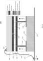
- FIG. 24 One typical cross-sectional view of the chip (IC stack) is shown in Figure 24 as an example to set the stage for the description of the placement of the duplexers in the IC metal layer stack.
- the package on which the belly of the IC may be placed is a ground plane layer 2420 of the package or the PCB.
- the ground layer 2420 is connected through the external bond wires 2412.
- the thick substrate 2418 is positioned at the bottom above the thin ground layer 2420 of the package or PCB.
- the conductor layers are connected through vias 2414, 2424 and 2426 to the transmitter and recei ver at the bottom of the IC.
- the top thick metallic layer 2402 can be used for AoC. This type of IC stack can host a large number of single or even multilayered duplexer structures.
- a T-shaped EIT-based planar duplexer 2500 is shown in Figures 25 according to aspects of the invention.
- the overall size may be 3x2.1 mm 2 at sub 6GHz frequencies, for example.
- the duplexer 2500 consists of two EIT filters tuned at different frequencies: the first filter is comprised of stubs 2506 and 2508, and the second filter is comprised of stubs 2512 and 2514.
- the length of stub 2506 is 1.9 mm
- stub 2508 is 1.7 mm
- stub 2512 is 1.5 mm
- stub 2514 is 1.3 mm.
- the width of stubs 2506, 2508 is 0.05 mm and the width of stubs 2512 and 2514 is 0.06mm.
- the width of microstrip 2502 and 2518 is 0.12 mm.
- the filter with a larger length (2506, 2508) resonates at relatively lower frequency ranges, and the filter with a shorter length (2512, 2514) resonates at relatively higher frequency ranges.
- the duplexer action of duplexer 2500 is shown in the frequency response graph 2600 of Figure 26 which shows passbands 2610 and 2612 and stopbands 2618, 2620, 2622, and 2624.
- a typical EIT-based filter generally offers inferior out of the band rejection.
- Fano-based filters are one of the potential candidates in such a scenario.
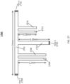
- a Fano-based duplexer 2700 is shown in Figure 27 .
- both open stubs of the first filter (2706, 2708) and of the second filter (2712, 2714) of Fano-based duplexer 2700 are of the same length.
- the length of stubs 2706 and 2708 is 1.2 mm; while stubs 2712 and 2714 are of 1.05 mm in length.
- the width of all of the open stubs of Fano-based duplexer 2700 is 0.05 mm.
- the width of stubs 2702 and 2718 is 0.12 mm.
- the frequency response of the T-shaped Fano filters of Fano-based duplexer 2700 is shown in the frequency response graph 2800 of Figure 28 which shows passbands 2810 and 2814 having a high-quality factor and also shows stopbands 2806, 2808, 2812, and 2816.
- Lorentzian filters can also be deployed in a T-shaped duplexer as shown in duplexer 2900 of Figure 29A .
- the pair of open stubs 2906 and 2908, and the pair of open stubs 2912 and 2914 are short-circuited in such a way that they each mimic a U-shape structure.
- the width of microstrip 2902 and 2918 is 0.21 mm and the width of stubs 2908 and 2914 is 0.1 mm.
- the overall length of microstrip 2902 is 3 mm.
- the frequency response of duplexer 2900 is shown in the frequency response graph 3000 of Figure 30 which shows passbands 3004 and 3012 and stopbands 3010 and 3014.
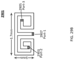
- the Lorentzian-based duplexers offer significant advantages over the EIT and Fano based duplexers because the Lorentzian-based duplexers provide good isolation and the U-shaped duplexer can also be changed to a spiral shape to decrease the size of the duplexer as shown in Figure 29B . Based on the above presented results, one can see the trade-off between different designs. For high selectivity, Fano-based filters are suitable; while for large bandwidth, FIT-based filters are recommended; and for high out-of-band rejection the Lorentzian-based filters appear to be the best choice.
- FIG. 31 A 3D view of a T-shaped duplexer is shown in Figure 31 in which vias 3104, 3118 connect the duplexer to the transmitter and the receiver that are fabricated in the epitaxial layer of the substrate.
- the array of the vias 3112 connects the port to the antenna at the top layer of the IC stack.
- vias are made up of tungsten (W) or other known materials that have a high resistivity. Therefore, multiple vias in parallel may be used to reduce the effective resistance.
- the stub size is close to ⁇ /4 in the stub-based T-type duplexers.
- the size of the stub is in the order of mm, which is large for the MMIMO system where one has to integrate a large number of the duplexers on a single chip.
- Such type of duplexers are therefore good candidates for the upper mm-wave frequencies (>50GHz) or THz frequencies.
- a 5G/6G design typically has components like an antenna, a duplexer, a time switch, filters, a mixed-signal ADC/DAC and a baseband processor provided on the same chip.
- the quality factor and width of the microstrips used to design the passive components depend on the thickness of the CMOS metal stack and resistivity of the substrate. It is recommended to use a high resistivity substrate to not only reduce the resistive losses in passive on-chip structures but also increase the radiation efficiency of the on-chip antennas. However, in the standard bulk CMOS process, the resistivity of the substrate is optimized to reduce the possibility of the latch-up in the CMOS transistors.
- resonators with a high-quality factor are preferred to reduce the insertion loss. Therefore, thin substrates are more suitable in mm-wave resonators.
- the thin substrate with a controlled resistivity makes it possible to design narrow microstrip structures with the same intrinsic impedances. As discussed earlier, a MMIMO chip might have 4 to 512 antennas, thus the same number of duplexers will be needed.
- Most commonly used on-chip antennas are planar monopole, patch, dipole, loop and Yagi-Uda antennas as shown in Figures 22A to 22C .
- the microstrip patch antennas are most commonly used for the on-chip antenna arrays.
- the planar nature and compact size make patch antenna make them a suitable candidate for on-chip antenna arrays.
- Each antenna will have a dedicated duplexer for communication with a receiver and a transmitter.
- the dimension of a patch antenna at 28 GHz with a dielectric SiO 2 permittivity of 4 is approximately 3x2 mm 2 .
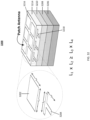
- the size of the duplexer should be equal to or less than the size of the antenna on the top metal layer of the chip as shown by the comparison of patch antenna 3202 to duplexer 3204 in the IC stack of Figure 32 .
- any microwave structure with relatively small dimensions resonates at higher frequencies; therefore, the scalability phenomena observed for Fano structures as presented in Figure 34 is also applicable to FIT and Lorentz structures.
- 300 GHz is not an upper limit, rather, the above-mentioned microstructures can resonate at higher frequencies even in the THz by reducing their dimensions in the appropriate range.
- the dimensions given in Figures 25 to 29 are scalable with frequency, but they are not linearly scalable. 3D electromagnetic optimization techniques are needed to attain the desired results at certain frequency bands. These dimensions are presented only as an example case and all the above-presented structures are scalable for mm-Wave and THz-frequencies.
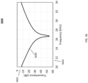
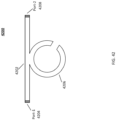
- a miniature proposed design using a simple ring resonator 3506 with a microstrip feed line 3502 is shown in Figure 35 and its frequency response is shown in the frequency response graph 3600 of Figure 36 .
- One possible variation is the use of split-ring resonator 3706 instead of a ring resonator 3506 as shown in Figure 37 .
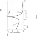
- the frequency response of the split-ring resonator 3706 design is shown in the frequency response graph 4000 of Figure 40 .
- Lorentz absorption at microwave frequencies can be achieved by using different methods like placing a resonating cavity near a microstrip as shown in Figure 35 .
- the size of resonators can be further decreased by increasing the dielectric permittivity of the substrate if possible.
- EIT, Fano, and Lorentz profiles can also be attained using the different combinations of the partial split-ring resonator and partial reflecting area in the microstrip line as shown in Figures 37 to 45 , respectively.
- the effectiveness of such type of passive solutions is that their size is equal to or even smaller than that of the size of the on-chip feeding antenna (as described above with regard to Figure 32 ) which makes them suitable for lower band mm-wave (20GH-50GHz) applications as well as higher frequencies.
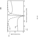
- the Fano resonance can be achieved by making a precise cut at the bottom of ring 3706 as shown in Figure 37 or making a partial reflection path 3802 in microstrip as shown in Figure 38 .
- the transparency window can be created in the absorption spectra as shown in the frequency response graph 3900 of Figure 39 .
- This high selectivity can provide the desired duplexing action at the channel or sub-band level in 5G/6G systems.
- the sizes of these filters are much smaller compared to the stub-based filter shown in Figure 10 .
- the frequency response is shown in the frequency response graph 4000 of Figure 40 with a quality factor of more than 500.
- the quality factor has a direct tradeoff with the bandwidth and can be adjusted to a desired value as depicted in the frequency response graph 4100 of Figure 41 .
- a large bandwidth can be achieved by using EIT instead of Fano resonance in the same split ring structure as shown in the Figure 43 inset.
- the phenomenon is the same as that shown in Figure 8 with an open stub.
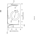
- the EIT phenomenon is achieved by placing two resonators with slightly different resonance frequencies adjacent to each other. This can be accomplished by shifting the gap from bottom of the ring to the right of the ring as shown in ring 4206 of Figure 42 .
- the resulting frequency response for ring 4206 is shown in the frequency response graph 4300 of Figure 43 .
- the Q factor and bandwidth can be controlled by changing the location of the gap ( ⁇ 1) 4414 in ring 4410 as shown in Figure 43 .
- the drawback of using this type of EIT based filtering is that it has poor out-of-band rejection, which means that these types of designs are not suitable where high selectivity is desired like in the case of DoCs needed for the sub-band selection.
- Moderate out-of-band rejection can be achieved by using traditional Lorentzian resonance which can be attained by inserting a cut both in the ring 4506 and in the transmission line 4502 as shown in Figure 45 .
- the frequency response of such a design is shown in the frequency response graph 4600 of Figure 46 .
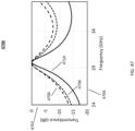
- the Lorentzian filter out-of-band rejection and Q factor can be improved, as shown in the frequency response graph 4700 of Figure 47 , by changing the width of the microstrip and the overlapping area between the ring and microstrip.
- Table 2 Effect of dielectric losses on the signal attenuation response of EIT, Fano, and Lorentz type filters structures Dielectric Loss (tan ⁇ ) Insertion Loss (dB) Fano Lorentzian EIT 0.000 (Ideal) 0.0 0.0 0.0 0.0001 -0.901 -0.065 -0.013 0.0003 -2.5 -0.195 -0.0186 0.0005 -3.859 -0.314 -0.086 0.0009 -6.061 -0.564 -0.163 0.001 -6.54 -0.625 -0.343 0.003 -12.915 -1.742 -0.536 0.009 -21.663 -4.439 -1.534
- the ring resonator based EIT, Fano, and Lorentz type filters are applied in the T-Shaped duplexer shown in Figure 20 .
- the basic structure of the transmission line remains the same for all designs. It is important to note that just by changing the position of the cut in the split ring resonator, the Fano, EIT and Lorentz responses can be achieved.
- split ring resonators which mimic an LC tank.
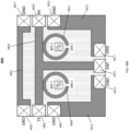
- the planar geometrical structure using a split ring resonator design is shown in Figure 48A .
- the design is similar to that of the one shown in Figure 20 , but with a different configuration that is smaller in size.
- the top view of such a design is shown in Figure 48A which shows the duplexer size is only 3 ⁇ 1 mm 2 .
- Fano, EIT, and Lorentzian Three different types of resonance phenomenon (Fano, EIT, and Lorentzian) are used to achieve the duplexing action.
- the frequency response of Fano, EIT, and Lorentz DoCs are shown in the frequency response graphs of Figures 49 , 50 and 51 , respectively.
- the Fano-based duplexer offers selectivity and isolation of approximately 25-30 dB; while EIT-based duplexers offer a relatively large bandwidth with low out-of-band rejection.
- Lorentzian resonance-based duplexers provide excellent out-of-band rejection and their isolation is independent of the position of resonances.
- the quality factor of EIT and Lorentz based DoCs is low compared to Fano-based DoCs.
- the EIT and Lorentzian based designs are useful at the front-end where large bandwidth is desired for the complete band.
- the Fano-based design is more suitable for the selection and duplexing of sub-bands.
- the aforementioned designs utilize simple and planar structures, and due to their small size they can fit under the AoC for the 28-32 GHz low band mm-wave applications. Maximum isolation of -30 dB with an insertion loss of up to 0.5 dB can be attained using the aforementioned structures.
- the aforementioned designs are flexible because both the selectivity and isolation can be controlled thereby adding another dimension to the novelty of the structure.
- FIGS 48A and 48B are planar and use the same metal layer of the CMOS metal stack. Using more than one metal layer, the design geometry can be reduced to realize even more compact structure.
- a Fano based duplexer was designed with a ring resonator diameter of 1 mm. This type of duplexer with a ring resonator has a better potential to be integrated on chip due to its small size.
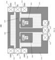
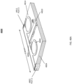
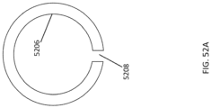
- the metal vias models were used to excite the resonators that were placed on the adjacent layers as shown in Figures 52A and 52B . In Figure 52B , antenna port-1 5204 and common ground port 5220 are shown.
- the signal that is received at receive port-2 5202 and transmit port-3 5218 depends upon the resonance frequencies of relevant SRRs.
- the common ground plane 5212 between both resonators 5210 and 5216 is connected with the package ground through multiple vias.
- the thickness of the dielectric between two metal layers is taken to be 9 ⁇ m.
- the duplexer action is achieved by tuning each of the SRR filters to a different frequency as shown in the frequency response graph 5300 of Figure 53 .
- the simulation results validate the concept of a folded multilayer duplexer as described above.
- the duplexer size can be further reduced which thereby makes the complete DoC of comparable dimension as that of SRR 5206 with a radius of 0.5mm.
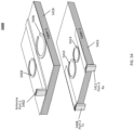
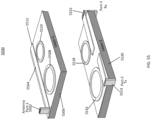
- FIGs 54 , 55 and 56 three multilayer DoC designs are shown. These designs utilize multiple spilt ring resonators (SRRs) at different frequencies to attain the near field coupling to attain the Fano, EIT and Lorentz resonance at the same time. These structures work on the same principle and provide a similar response as that of the planar DoC shown in Figure 52B . These designs provide similar tradeoffs in bandwidth, loss, and out-of-band rejection as that of the planar SRR-based DoC.
- SRRs spilt ring resonators
- FIG. 56 A new class of the Lorentz-based, double-spiral type of duplexer suitable for a single or multilayer implementation is shown in Figure 56 .
- the design is unique in its compactness and is suitable for the designs where an extremely large number of the DOCs are desired on a single chip.
- the frequency response of this design is shown in the frequency response graph 5700 of Figure 57 which shows the wide bandwidth and moderate selectivity which are typical characteristics of the Lorentz-based structures
- the array antenna 5838 has 16 AoC antennas (but it should be appreciated that the number of these antennas could reach up to 1000) and each antenna is connected with a dedicated duplexer 5834 and 5836.
- the signal from the duplexer (5834 or 5836) passes through single pole multiple throw (SPMT) switches which are connected with the sets of BP filters 5840 and 5842. These SPMT switches are further connected to the power amplifier 5812 and LNA 5816.
- the BP filters 5840 and 5842 provide sub-band selection.
- BP filters are important for the cognitive functionality inherent in the 5G/6G radios for the dynamic selection of an available frequency band for transmission and for reception.
- BP filters can be EIT, Fano or the Lorentz type and can be realized using the open stubs or the SRR structures described above and in the accompanying figures.
- the uplink and downlink can have different data rates and that translates to different bandwidth requirements in the associated cognitive radios.
- the cognitive radio allocates the software and hardware resources dynamically to optimally utilize the available resources in order to meet the user demands at the same time.
- filters 5910 and 5912 for the uplink and the downlink as shown in Figure 59 and thereby achieve the different bandwidths on the uplink and the downlink.
- the filters 5910 and 5912 can be of the EIT, Fano or Lorentzian type. These filters have different selectivity and out-of-band rejection and the appropriate filter can be chosen to meet the requirement for a given application.
- Such asymmetric duplexers may be used in bands where part of the uplink band is intentionally left unused to avoid interference in adjacent bands, such as when using the C and D blocks of the WCS frequency band, for example.
- Such asymmetric duplexers may also be used when implementing channel aggregation, such as may occur in LTE Advanced systems, thereby causing the downlink to have a wider bandwidth than the uplink bandwidth.
Landscapes
- Physics & Mathematics (AREA)
- Electromagnetism (AREA)
- Control Of Motors That Do Not Use Commutators (AREA)
- Optical Communication System (AREA)
- Silicon Compounds (AREA)
Applications Claiming Priority (4)
| Application Number | Priority Date | Filing Date | Title |
|---|---|---|---|
| US202063093771P | 2020-10-19 | 2020-10-19 | |
| US17/198,712 US11424525B2 (en) | 2020-10-19 | 2021-03-11 | Duplexers and related devices for 5G/6G and subsequent protocols and for mm-wave and terahertz applications |
| PCT/US2021/054093 WO2022086725A1 (en) | 2020-10-19 | 2021-10-08 | Duplexers and related devices for 5g/6g and subsequent protocols and for mm-wave and terahertz applications |
| EP21883543.7A EP4229715A1 (de) | 2020-10-19 | 2021-10-08 | Duplexer und zugehörige vorrichtungen für 5g/6g und nachfolgende protokolle und für mm-wellen- und terahertzanwendungen |
Related Parent Applications (2)
| Application Number | Title | Priority Date | Filing Date |
|---|---|---|---|
| EP21883543.7A Division-Into EP4229715A1 (de) | 2020-10-19 | 2021-10-08 | Duplexer und zugehörige vorrichtungen für 5g/6g und nachfolgende protokolle und für mm-wellen- und terahertzanwendungen |
| EP21883543.7A Division EP4229715A1 (de) | 2020-10-19 | 2021-10-08 | Duplexer und zugehörige vorrichtungen für 5g/6g und nachfolgende protokolle und für mm-wellen- und terahertzanwendungen |
Publications (1)
| Publication Number | Publication Date |
|---|---|
| EP4274039A2 true EP4274039A2 (de) | 2023-11-08 |
Family
ID=81185609
Family Applications (2)
| Application Number | Title | Priority Date | Filing Date |
|---|---|---|---|
| EP21883543.7A Withdrawn EP4229715A1 (de) | 2020-10-19 | 2021-10-08 | Duplexer und zugehörige vorrichtungen für 5g/6g und nachfolgende protokolle und für mm-wellen- und terahertzanwendungen |
| EP23181886.5A Withdrawn EP4274039A2 (de) | 2020-10-19 | 2021-10-08 | Duplexer und zugehörige vorrichtungen für 5g/6g und nachfolgende protokolle und für mm-wellen- und terahertzanwendungen |
Family Applications Before (1)
| Application Number | Title | Priority Date | Filing Date |
|---|---|---|---|
| EP21883543.7A Withdrawn EP4229715A1 (de) | 2020-10-19 | 2021-10-08 | Duplexer und zugehörige vorrichtungen für 5g/6g und nachfolgende protokolle und für mm-wellen- und terahertzanwendungen |
Country Status (5)
| Country | Link |
|---|---|
| US (2) | US11424525B2 (de) |
| EP (2) | EP4229715A1 (de) |
| AU (1) | AU2021364112A1 (de) |
| CA (1) | CA3191090A1 (de) |
| WO (1) | WO2022086725A1 (de) |
Families Citing this family (4)
| Publication number | Priority date | Publication date | Assignee | Title |
|---|---|---|---|---|
| WO2021120125A1 (en) * | 2019-12-19 | 2021-06-24 | Huawei Technologies Co., Ltd. | Antenna apparatus and bases tation |
| US12009849B2 (en) * | 2021-08-25 | 2024-06-11 | Apple Inc. | Distributed-element filter for mmWave frequencies |
| US20250233723A1 (en) * | 2024-01-17 | 2025-07-17 | Prince Sattam Bin Abdulaziz University (PSAU) | Fano based time division duplexing switch |
| CN117907349B (zh) * | 2024-03-19 | 2024-05-24 | 成都信息工程大学 | 一种便携式材料微小缺陷射频检测系统及检测方法 |
Citations (5)
| Publication number | Priority date | Publication date | Assignee | Title |
|---|---|---|---|---|
| EP0928064A2 (de) | 1991-10-28 | 1999-07-07 | Fujitsu Limited | Akustiches Oberflächenwellenfilter |
| US7038551B2 (en) | 2002-05-16 | 2006-05-02 | Tdk Corporation | Antenna duplexer |
| US20070139135A1 (en) | 2005-12-20 | 2007-06-21 | Xytrans, Inc. | Waveguide diplexer |
| EA021016B1 (ru) | 2012-02-03 | 2015-03-31 | Федеральное Государственное Автономное Образовательное Учреждение Высшего Профессионального Образования "Сибирский Федеральный Университет" | Микрополосковый диплексер |
| US9203373B2 (en) | 2013-01-11 | 2015-12-01 | Qualcomm Incorporated | Diplexer design using through glass via technology |
Family Cites Families (11)
| Publication number | Priority date | Publication date | Assignee | Title |
|---|---|---|---|---|
| AU470870B2 (en) * | 1973-10-29 | 1976-04-01 | Matsushita Electric Industrial Co., Ltd. | Filters employing elements with distributed constants |
| FR2512281B1 (de) | 1981-08-28 | 1983-10-28 | Thomson Csf | |
| US5023866A (en) * | 1987-02-27 | 1991-06-11 | Motorola, Inc. | Duplexer filter having harmonic rejection to control flyback |
| US6326866B1 (en) * | 1998-02-24 | 2001-12-04 | Murata Manufacturing Co., Ltd. | Bandpass filter, duplexer, high-frequency module and communications device |
| JP3861806B2 (ja) * | 2001-12-18 | 2006-12-27 | 株式会社村田製作所 | 共振器、フィルタ、デュプレクサ、および通信装置 |
| DE10238523B4 (de) * | 2002-08-22 | 2014-10-02 | Epcos Ag | Verkapseltes elektronisches Bauelement und Verfahren zur Herstellung |
| US8294538B2 (en) * | 2007-03-05 | 2012-10-23 | National University Corporation Kyoto Institute Of Technology | Transmission line microwave apparatus including at least one non-reciprocal transmission line part between two parts |
| US8358182B2 (en) * | 2009-02-05 | 2013-01-22 | Ecole De Technologie Superieure | Duplexer for integration in communication terminals |
| US7884991B1 (en) * | 2009-07-21 | 2011-02-08 | National Tsing Hua University | Structure and method for realizing electromagnetically-induced transparency |
| US10186743B2 (en) * | 2017-01-30 | 2019-01-22 | United Arab Emirates University | Microstrip circuits exhibiting electromagnetically induced transparency and fano resonance |
| US10186744B2 (en) | 2017-02-06 | 2019-01-22 | United Arab Emirates University | Microstrip Fano resonator switch |
-
2021
- 2021-03-11 US US17/198,712 patent/US11424525B2/en active Active
- 2021-10-08 EP EP21883543.7A patent/EP4229715A1/de not_active Withdrawn
- 2021-10-08 EP EP23181886.5A patent/EP4274039A2/de not_active Withdrawn
- 2021-10-08 WO PCT/US2021/054093 patent/WO2022086725A1/en not_active Ceased
- 2021-10-08 AU AU2021364112A patent/AU2021364112A1/en not_active Abandoned
- 2021-10-08 CA CA3191090A patent/CA3191090A1/en active Pending
-
2022
- 2022-05-13 US US17/743,904 patent/US11764456B2/en active Active
Patent Citations (5)
| Publication number | Priority date | Publication date | Assignee | Title |
|---|---|---|---|---|
| EP0928064A2 (de) | 1991-10-28 | 1999-07-07 | Fujitsu Limited | Akustiches Oberflächenwellenfilter |
| US7038551B2 (en) | 2002-05-16 | 2006-05-02 | Tdk Corporation | Antenna duplexer |
| US20070139135A1 (en) | 2005-12-20 | 2007-06-21 | Xytrans, Inc. | Waveguide diplexer |
| EA021016B1 (ru) | 2012-02-03 | 2015-03-31 | Федеральное Государственное Автономное Образовательное Учреждение Высшего Профессионального Образования "Сибирский Федеральный Университет" | Микрополосковый диплексер |
| US9203373B2 (en) | 2013-01-11 | 2015-12-01 | Qualcomm Incorporated | Diplexer design using through glass via technology |
Also Published As
| Publication number | Publication date |
|---|---|
| US20220278434A1 (en) | 2022-09-01 |
| CA3191090A1 (en) | 2022-04-28 |
| US20220123453A1 (en) | 2022-04-21 |
| AU2021364112A1 (en) | 2023-03-09 |
| WO2022086725A1 (en) | 2022-04-28 |
| US11764456B2 (en) | 2023-09-19 |
| US11424525B2 (en) | 2022-08-23 |
| EP4229715A1 (de) | 2023-08-23 |
Similar Documents
| Publication | Publication Date | Title |
|---|---|---|
| US11764456B2 (en) | Duplexers and related devices for 5G/6G and subsequent protocols and for mm-wave and terahertz applications | |
| US8373603B2 (en) | Dual feed antenna | |
| KR101119228B1 (ko) | 메타물질 구조에 기반한 안테나, 장치 및 시스템 | |
| US10062949B2 (en) | Integrated multi-band bandpass filters based on dielectric resonators for mobile and other communication devices and applications | |
| Dong et al. | Development of ultrawideband antenna with multiple band-notched characteristics using half mode substrate integrated waveguide cavity technology | |
| DE102018214860A1 (de) | Elektronische Vorrichtung mit mehreren Antennen mit gemeinsamen Strukturen für Nahfeld-Kommunikation und Nicht-Nahfeld-Kommunikation | |
| CN104882677B (zh) | 具有高共模抑制比的差分缝隙mimo天线 | |
| TW201635647A (zh) | 可重組的多頻多功能天線 | |
| EP3416241A1 (de) | Monopolantenne | |
| Mishra et al. | Filtennas for wireless application: A review | |
| EP2926410A1 (de) | Gefalteten metainspirierte dualbandantenne mit in eine benutzervorrichtung eingebetteten breitbandeigenschaften | |
| Rodrigues et al. | The application of reconfigurable filtennas in mobile satellite terminals | |
| CN111600130A (zh) | 一种去耦芯片 | |
| WO2013175903A1 (ja) | アンテナ装置及びmimo無線装置 | |
| KR20230067692A (ko) | 안테나 디바이스, 안테나 디바이스들의 어레이 | |
| Anuvind et al. | 2× 2 MIMO antenna at 2.4 GHz for WLAN applications | |
| CN105576372A (zh) | 一种小型化差分陷波uwb-mimo天线 | |
| CN112510366A (zh) | 一种级联式去耦芯片 | |
| CN105305052B (zh) | 差分阶梯馈电的高矩形度陷波超宽带缝隙天线 | |
| Alhegazi et al. | Review of recent developments in filtering-antennas | |
| CN113851845A (zh) | 一种抑制带内信号的集成滤波双工天线 | |
| Ikhyari et al. | Design and characterization of ADM-based dual-band SIW bandpass filter | |
| Abdelhamid et al. | A new multi-antenna MIMO for X-band satellite communications | |
| CN112510368B (zh) | 一种可调谐双频去耦芯片 | |
| CN120415473A (zh) | 射频系统及电子设备 |
Legal Events
| Date | Code | Title | Description |
|---|---|---|---|
| PUAI | Public reference made under article 153(3) epc to a published international application that has entered the european phase |
Free format text: ORIGINAL CODE: 0009012 |
|
| STAA | Information on the status of an ep patent application or granted ep patent |
Free format text: STATUS: THE APPLICATION HAS BEEN PUBLISHED |
|
| AC | Divisional application: reference to earlier application |
Ref document number: 4229715 Country of ref document: EP Kind code of ref document: P |
|
| AK | Designated contracting states |
Kind code of ref document: A2 Designated state(s): AL AT BE BG CH CY CZ DE DK EE ES FI FR GB GR HR HU IE IS IT LI LT LU LV MC MK MT NL NO PL PT RO RS SE SI SK SM TR |
|
| STAA | Information on the status of an ep patent application or granted ep patent |
Free format text: STATUS: THE APPLICATION HAS BEEN WITHDRAWN |
|
| 18W | Application withdrawn |
Effective date: 20231106 |