EP4277290A2 - Kamerakopf - Google Patents
Kamerakopf Download PDFInfo
- Publication number
- EP4277290A2 EP4277290A2 EP23195498.3A EP23195498A EP4277290A2 EP 4277290 A2 EP4277290 A2 EP 4277290A2 EP 23195498 A EP23195498 A EP 23195498A EP 4277290 A2 EP4277290 A2 EP 4277290A2
- Authority
- EP
- European Patent Office
- Prior art keywords
- pcbs
- pcb
- camera head
- video camera
- solid state
- Prior art date
- Legal status (The legal status is an assumption and is not a legal conclusion. Google has not performed a legal analysis and makes no representation as to the accuracy of the status listed.)
- Pending
Links
Images


Classifications
-
- H—ELECTRICITY
- H05—ELECTRIC TECHNIQUES NOT OTHERWISE PROVIDED FOR
- H05K—PRINTED CIRCUITS; CASINGS OR CONSTRUCTIONAL DETAILS OF ELECTRIC APPARATUS; MANUFACTURE OF ASSEMBLAGES OF ELECTRICAL COMPONENTS
- H05K1/00—Printed circuits
- H05K1/02—Details
- H05K1/14—Structural association of two or more printed circuits
- H05K1/144—Stacked arrangements of planar printed circuit boards
-
- A—HUMAN NECESSITIES
- A61—MEDICAL OR VETERINARY SCIENCE; HYGIENE
- A61B—DIAGNOSIS; SURGERY; IDENTIFICATION
- A61B1/00—Instruments for performing medical examinations of the interior of cavities or tubes of the body by visual or photographical inspection, e.g. endoscopes; Illuminating arrangements therefor
- A61B1/04—Instruments for performing medical examinations of the interior of cavities or tubes of the body by visual or photographical inspection, e.g. endoscopes; Illuminating arrangements therefor combined with photographic or television appliances
- A61B1/05—Instruments for performing medical examinations of the interior of cavities or tubes of the body by visual or photographical inspection, e.g. endoscopes; Illuminating arrangements therefor combined with photographic or television appliances characterised by the image sensor, e.g. camera, being in the distal end portion
- A61B1/051—Details of CCD assembly
-
- A—HUMAN NECESSITIES
- A61—MEDICAL OR VETERINARY SCIENCE; HYGIENE
- A61B—DIAGNOSIS; SURGERY; IDENTIFICATION
- A61B1/00—Instruments for performing medical examinations of the interior of cavities or tubes of the body by visual or photographical inspection, e.g. endoscopes; Illuminating arrangements therefor
- A61B1/06—Instruments for performing medical examinations of the interior of cavities or tubes of the body by visual or photographical inspection, e.g. endoscopes; Illuminating arrangements therefor with illuminating arrangements
- A61B1/0607—Instruments for performing medical examinations of the interior of cavities or tubes of the body by visual or photographical inspection, e.g. endoscopes; Illuminating arrangements therefor with illuminating arrangements for annular illumination
-
- A—HUMAN NECESSITIES
- A61—MEDICAL OR VETERINARY SCIENCE; HYGIENE
- A61B—DIAGNOSIS; SURGERY; IDENTIFICATION
- A61B1/00—Instruments for performing medical examinations of the interior of cavities or tubes of the body by visual or photographical inspection, e.g. endoscopes; Illuminating arrangements therefor
- A61B1/06—Instruments for performing medical examinations of the interior of cavities or tubes of the body by visual or photographical inspection, e.g. endoscopes; Illuminating arrangements therefor with illuminating arrangements
- A61B1/0661—Endoscope light sources
- A61B1/0676—Endoscope light sources at distal tip of an endoscope
-
- A—HUMAN NECESSITIES
- A61—MEDICAL OR VETERINARY SCIENCE; HYGIENE
- A61B—DIAGNOSIS; SURGERY; IDENTIFICATION
- A61B1/00—Instruments for performing medical examinations of the interior of cavities or tubes of the body by visual or photographical inspection, e.g. endoscopes; Illuminating arrangements therefor
- A61B1/06—Instruments for performing medical examinations of the interior of cavities or tubes of the body by visual or photographical inspection, e.g. endoscopes; Illuminating arrangements therefor with illuminating arrangements
- A61B1/0661—Endoscope light sources
- A61B1/0684—Endoscope light sources using light emitting diodes [LED]
-
- G—PHYSICS
- G02—OPTICS
- G02B—OPTICAL ELEMENTS, SYSTEMS OR APPARATUS
- G02B23/00—Telescopes, e.g. binoculars; Periscopes; Instruments for viewing the inside of hollow bodies; Viewfinders; Optical aiming or sighting devices
- G02B23/24—Instruments or systems for viewing the inside of hollow bodies, e.g. fibrescopes
- G02B23/2407—Optical details
- G02B23/2423—Optical details of the distal end
- G02B23/243—Objectives for endoscopes
-
- G—PHYSICS
- G02—OPTICS
- G02B—OPTICAL ELEMENTS, SYSTEMS OR APPARATUS
- G02B23/00—Telescopes, e.g. binoculars; Periscopes; Instruments for viewing the inside of hollow bodies; Viewfinders; Optical aiming or sighting devices
- G02B23/24—Instruments or systems for viewing the inside of hollow bodies, e.g. fibrescopes
- G02B23/2407—Optical details
- G02B23/2461—Illumination
- G02B23/2469—Illumination using optical fibres
-
- G—PHYSICS
- G02—OPTICS
- G02B—OPTICAL ELEMENTS, SYSTEMS OR APPARATUS
- G02B23/00—Telescopes, e.g. binoculars; Periscopes; Instruments for viewing the inside of hollow bodies; Viewfinders; Optical aiming or sighting devices
- G02B23/24—Instruments or systems for viewing the inside of hollow bodies, e.g. fibrescopes
- G02B23/2476—Non-optical details, e.g. housings, mountings, supports
- G02B23/2484—Arrangements in relation to a camera or imaging device
-
- H—ELECTRICITY
- H04—ELECTRIC COMMUNICATION TECHNIQUE
- H04N—PICTORIAL COMMUNICATION, e.g. TELEVISION
- H04N23/00—Cameras or camera modules comprising electronic image sensors; Control thereof
- H04N23/57—Mechanical or electrical details of cameras or camera modules specially adapted for being embedded in other devices
-
- H—ELECTRICITY
- H05—ELECTRIC TECHNIQUES NOT OTHERWISE PROVIDED FOR
- H05K—PRINTED CIRCUITS; CASINGS OR CONSTRUCTIONAL DETAILS OF ELECTRIC APPARATUS; MANUFACTURE OF ASSEMBLAGES OF ELECTRICAL COMPONENTS
- H05K2201/00—Indexing scheme relating to printed circuits covered by H05K1/00
- H05K2201/04—Assemblies of printed circuits
- H05K2201/042—Stacked spaced PCBs; Planar parts of folded flexible circuits having mounted components in between or spaced from each other
-
- H—ELECTRICITY
- H05—ELECTRIC TECHNIQUES NOT OTHERWISE PROVIDED FOR
- H05K—PRINTED CIRCUITS; CASINGS OR CONSTRUCTIONAL DETAILS OF ELECTRIC APPARATUS; MANUFACTURE OF ASSEMBLAGES OF ELECTRICAL COMPONENTS
- H05K2201/00—Indexing scheme relating to printed circuits covered by H05K1/00
- H05K2201/09—Shape and layout
- H05K2201/09009—Substrate related
- H05K2201/09027—Non-rectangular flat PCB, e.g. circular
-
- H—ELECTRICITY
- H05—ELECTRIC TECHNIQUES NOT OTHERWISE PROVIDED FOR
- H05K—PRINTED CIRCUITS; CASINGS OR CONSTRUCTIONAL DETAILS OF ELECTRIC APPARATUS; MANUFACTURE OF ASSEMBLAGES OF ELECTRICAL COMPONENTS
- H05K2201/00—Indexing scheme relating to printed circuits covered by H05K1/00
- H05K2201/10—Details of components or other objects attached to or integrated in a printed circuit board
- H05K2201/10007—Types of components
- H05K2201/10106—Light emitting diode [LED]
-
- H—ELECTRICITY
- H05—ELECTRIC TECHNIQUES NOT OTHERWISE PROVIDED FOR
- H05K—PRINTED CIRCUITS; CASINGS OR CONSTRUCTIONAL DETAILS OF ELECTRIC APPARATUS; MANUFACTURE OF ASSEMBLAGES OF ELECTRICAL COMPONENTS
- H05K2201/00—Indexing scheme relating to printed circuits covered by H05K1/00
- H05K2201/10—Details of components or other objects attached to or integrated in a printed circuit board
- H05K2201/10007—Types of components
- H05K2201/10121—Optical component, e.g. opto-electronic component
-
- H—ELECTRICITY
- H05—ELECTRIC TECHNIQUES NOT OTHERWISE PROVIDED FOR
- H05K—PRINTED CIRCUITS; CASINGS OR CONSTRUCTIONAL DETAILS OF ELECTRIC APPARATUS; MANUFACTURE OF ASSEMBLAGES OF ELECTRICAL COMPONENTS
- H05K2201/00—Indexing scheme relating to printed circuits covered by H05K1/00
- H05K2201/10—Details of components or other objects attached to or integrated in a printed circuit board
- H05K2201/10007—Types of components
- H05K2201/10151—Sensor
-
- H—ELECTRICITY
- H05—ELECTRIC TECHNIQUES NOT OTHERWISE PROVIDED FOR
- H05K—PRINTED CIRCUITS; CASINGS OR CONSTRUCTIONAL DETAILS OF ELECTRIC APPARATUS; MANUFACTURE OF ASSEMBLAGES OF ELECTRICAL COMPONENTS
- H05K2201/00—Indexing scheme relating to printed circuits covered by H05K1/00
- H05K2201/10—Details of components or other objects attached to or integrated in a printed circuit board
- H05K2201/10227—Other objects, e.g. metallic pieces
- H05K2201/10295—Metallic connector elements partly mounted in a hole of the PCB
- H05K2201/10303—Pin-in-hole mounted pins
-
- H—ELECTRICITY
- H05—ELECTRIC TECHNIQUES NOT OTHERWISE PROVIDED FOR
- H05K—PRINTED CIRCUITS; CASINGS OR CONSTRUCTIONAL DETAILS OF ELECTRIC APPARATUS; MANUFACTURE OF ASSEMBLAGES OF ELECTRICAL COMPONENTS
- H05K2201/00—Indexing scheme relating to printed circuits covered by H05K1/00
- H05K2201/10—Details of components or other objects attached to or integrated in a printed circuit board
- H05K2201/10227—Other objects, e.g. metallic pieces
- H05K2201/1031—Surface mounted metallic connector elements
- H05K2201/10318—Surface mounted metallic pins
-
- H—ELECTRICITY
- H05—ELECTRIC TECHNIQUES NOT OTHERWISE PROVIDED FOR
- H05K—PRINTED CIRCUITS; CASINGS OR CONSTRUCTIONAL DETAILS OF ELECTRIC APPARATUS; MANUFACTURE OF ASSEMBLAGES OF ELECTRICAL COMPONENTS
- H05K2201/00—Indexing scheme relating to printed circuits covered by H05K1/00
- H05K2201/20—Details of printed circuits not provided for in H05K2201/01 - H05K2201/10
- H05K2201/2036—Permanent spacer or stand-off in a printed circuit or printed circuit assembly
Definitions
- the invention is from the field of video cameras. Specifically the invention relates to small diameter camera heads for use in such applications as medical endoscopes and laparoscopes and industrial borescopes.
- a third obstacle connected with small diameter camera heads such as those described in WO2011/033513 is the difficulty of assembly, in particular connecting the internal wiring, which is not suitable to mass production manufacturing.
- a fourth obstacle is related to the need of integrated illumination in the aforementioned devices and the difficulty of transferring adequate amounts of current while maintaining the minimal dimensions of the camera-illumination assembly.
- the invention is a video camera head comprised of at least two rigid printed circuit boards (PCBs) arranged in parallel planes.
- the PCBs are mechanically supported one above the other by pins made of an electricity conducting material.
- the pins conduct electrical power from the bottom PCB to electronic components and/or illumination means mounted on the other PCBs of the at least two PCBs and signals from a sensor chip mounted on one of the other PCBs of the at least two PCBs to the bottom PCB.
- the illumination means comprise at least one LED, e.g. a ring array of LEDs.
- Embodiments of the video camera head of the invention comprise an objective optical system.
- the video camera head of the invention comprised of three PCBs components for receiving signals from a solid state sensor and outputting a video signal are mounted on the bottom PCB, a solid state sensor chip is mounted on the middle PCB, and an objective optical system and illumination means are mounted on the top PCB.
- Pins made of electricity conducting material (a) mechanically support the middle and top PCBs above the bottom PCB, (b) conduct electrical power from the bottom PCB to the middle and top PCBs, and (c) conduct signals from the sensor chip on the middle PCB to the bottom PCB.
- the video camera head of the invention comprised of two PCBs electronic components for receiving signals from a solid state sensor and outputting a video signal are mounted on the bottom PCB, a solid state sensor chip is mounted on the top side of the bottom PCB, and an objective optical system and illumination means are mounted on the top PCB.
- Pins made of electricity conducting material mechanically support the top PCB above the bottom PCB and conduct electrical power from the bottom PCB to top PCB.
- Through vias are provided to conduct electrical power from the bottom side to the top side of the bottom PCB and to conduct signals from the sensor chip on the top side to the bottom side of the bottom PCB.
- the video camera head of the invention comprised of four PCBs
- electronic components for receiving signals from a solid state sensor and outputting a video signal are mounted on the first (bottom) and second PCBs
- a solid state sensor chip is mounted on the third PCB
- an objective optical system and illumination means are mounted on the fourth (top) PCB.
- Pins made of electricity conducting material (a) mechanically support the second, third, and fourth PCBs above the first PCB, (b) conduct electrical power from the first PCB to the second, third, and fourth PCBs, and (c) conduct signals from the sensor chip on the third PCB to the first PCB.
- the invention is a video camera head comprised of at least two rigid printed circuit boards (PCBS) arranged in parallel planes.
- PCBS printed circuit boards
- an objective optical system and illumination means are mounted on the distal end of a housing of the camera head
- a solid state sensor chip is mounted on a PCB below the objective optical system
- electronic components for receiving signals from a solid state sensor and outputting a video signal are mounted on at least one of the PCBs
- the at least two PCBs are mechanically supported one above the other by electrically conducting pins
- the illumination means supported on the distal end of the camera housing are output couplers of optical fibers or the distal end of light guides.
- the light source for the illumination means of the video camera of the second aspect of the invention can be any conventional light source used with endoscopic systems.
- the light from the LEDs is transferred to the distal end of a housing of the camera head through hollow light guides.
- the light source is LEDs that are mounted on one of the PCBs in the camera head or proximally from it.
- the LEDs can be mounted on a PCB together with the solid state sensor chip. In other embodiments the LEDs are mounted on a PCB below the PCB on which the solid state sensor chip is mounted.
- the light source is located remotely from the camera head and the light is transferred directly from the light source to an output coupler on the distal end of the camera housing or to one of the PCBs where it is coupled into a hollow light guide.
- the pins can be either rigid or flexible.
- the PCBs are not circular and can have any shape, symmetric or non-symmetric.
- some or all of the PCBs in a camera head can be different from the shapes and dimensions of other PCBs in the camera head.
- some or all of the components of the objective optical system can be mounted on a housing of the camera head.
- Fig. 1 schematically shows the structure of an embodiment of the camera head (10) of the invention.
- This embodiment of the camera head of the present invention comprises three rigid PCBs (12a, 12b, and 12c).
- the three PCBs are arranged in three parallel planes one above the other. (Note that for convenience the camera head is described as if it were oriented with its central axis vertical. This defines the relative directions such as top and bottom used herein.)
- the middle PCB (12b) is mechanically supported above the lower PCB (12c) by six short pins (14) and the upper PCB (12a) is mechanically supported above the lower PCB (12c) by two longer pins (16) that pass through vias in PCB (12b). It is noted that embodiments of the camera head (10) may comprise more or less than 6 pins (14) and more than two pins (16).
- Metallization (18) is created on the surface of the lower PCB (12c) and electronic components (20) for receiving signals from a solid state image sensor, e.g. CMOS, and outputting a video signal are electrically connected to this metallization.
- a camera cable (30) that conducts power to the camera head and video signals from it to a remote signal processor is connected by means of through vias to the metallization pattern on the top side of PCB (12c).
- Middle PCB (12b) supports the solid state sensor chip (22).
- the upper PCB (12a) supports the objective optical system (24) inside its housing (26) and illumination means, e.g. at least one LED or a ring array of LEDs (28) surrounding housing (26).
- illumination means e.g. at least one LED or a ring array of LEDs (28) surrounding housing (26).
- Pins (14) and (16) are made of electricity conducting material. Therefore they serve the dual purpose of mechanically supporting the upper two PCBs and also of conducting power to and signals from the sensor chip (22) and power to LEDs 28.
- the internal structure of camera head (10) thus addresses all four of the obstacles discussed in the background section of this application. Firstly use of rigid PCBs instead of flexible PCBs eliminates the bending radius of the flexible PCB that usually increases the diameter of the camera head. Secondly the use of the electrically connecting pins allows for transferring adequate amounts of current for the illumination sources. Thirdly and fourthly the use of the electrically connecting pins eliminates most of the difficulty of making the internal wiring connections and therefore greatly simplifies the assembly process, thereby making camera head (10) into a device that is very suitable for mass production manufacturing.
- an embodiment of the camera head of the invention can comprise two PCBs in which case the electronic components are located on the bottom surface of the lower PCB and the sensor chip on the top surface of the bottom PCB and the objective lens system and illumination source on the upper PCB.
- Other embodiments can comprise more than three PCBs, for example four in which the lower two PCBs support electronic components, the third PCB supports the sensor chip and the top PCB supports the objective optical system and illumination means.
- electricity conducting pins serve the dual purposes of separating and mechanically supporting the PCBs and of conducting electric power and video signals between them.
- the illumination means supported on the uppermost PCB are output couplers of optical fibers or light guides.
- the light source can be any conventional light source used with endoscopic systems, e.g. LEDs that can be mounted on one of the lower PCBs in the camera head or proximally from it.
- the electrically conducting pins may be combined with hollow light guides.
- the camera head comprises three PCBs that are mechanically supported one above the other by electricity conducting pins 14,16.
- the two lower PCBs 12b,12c support electronic components (not shown in the figure) for receiving signals from a solid state image sensor 22 and outputting a video signal.
- the uppermost PCB 12a supports the solid state sensor 22 and one or more LEDs 28, e.g. a circular array, which surround the sensor.
- an objective lens system 24 enclosed in its housing 26 is held in place above the sensor 22 by a support structure, e.g. a hollow tube attached at its bottom end to the PCB 12a or by a structure attached to a camera housing 34 that surrounds the internal components of the camera head.
- the camera head also comprises vertical tubular light guides 32, which transfer light from the LEDs 28 to the height of the objective lens 24 on the distal end 36 of the camera housing 34 facing the object to be imaged.
- the light guides 32 are supported above the LEDs 28, for example by being attached at their bottom ends to the PCB 12a or by supports attached to the interior of the camera housing 34.
- the electronic components located on PCBs 12a and 12b can be redistributed onto one PCB only and/or some can be located on PCB 12a thereby allowing this embodiment of the camera head to comprise only two PCBs.
- camera cable 30 is connected to electronic components on the bottom PCB.
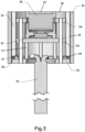
- FIG. 3 A variation of the embodiment shown in Fig. 2 is shown schematically in Fig. 3 .
- electronic components (not shown) are located on PCBs 12a and 12c (and in some versions also on 12b), the LEDs 28 are on PCB 12c and light guides 32 transfer light from the LEDs 28 to the height of the objective lens 24 the distal end 36 of the camera housing 34 facing the object to be imaged.
- the light source can be located remotely from the camera head and the light transferred directly from the light source to an output coupler on the distal end 36 of the camera housing 34 or alternately to one of the PCBs where it is coupled into a hollow light guide as shown in Figs. 2 and 3 .
Landscapes
- Health & Medical Sciences (AREA)
- Life Sciences & Earth Sciences (AREA)
- Physics & Mathematics (AREA)
- Surgery (AREA)
- Engineering & Computer Science (AREA)
- Optics & Photonics (AREA)
- Heart & Thoracic Surgery (AREA)
- Medical Informatics (AREA)
- Pathology (AREA)
- Radiology & Medical Imaging (AREA)
- Biophysics (AREA)
- Biomedical Technology (AREA)
- Nuclear Medicine, Radiotherapy & Molecular Imaging (AREA)
- Veterinary Medicine (AREA)
- Molecular Biology (AREA)
- Animal Behavior & Ethology (AREA)
- General Health & Medical Sciences (AREA)
- Public Health (AREA)
- Astronomy & Astrophysics (AREA)
- General Physics & Mathematics (AREA)
- Microelectronics & Electronic Packaging (AREA)
- Multimedia (AREA)
- Signal Processing (AREA)
- Endoscopes (AREA)
- Instruments For Viewing The Inside Of Hollow Bodies (AREA)
- Studio Devices (AREA)
- Transforming Light Signals Into Electric Signals (AREA)
Applications Claiming Priority (3)
| Application Number | Priority Date | Filing Date | Title |
|---|---|---|---|
| IL239386A IL239386B (en) | 2015-06-11 | 2015-06-11 | Video camera head |
| EP16807031.6A EP3308610B1 (de) | 2015-06-11 | 2016-06-09 | Kamerakopf |
| PCT/IL2016/050603 WO2016199143A1 (en) | 2015-06-11 | 2016-06-09 | Camera head |
Related Parent Applications (1)
| Application Number | Title | Priority Date | Filing Date |
|---|---|---|---|
| EP16807031.6A Division EP3308610B1 (de) | 2015-06-11 | 2016-06-09 | Kamerakopf |
Publications (2)
| Publication Number | Publication Date |
|---|---|
| EP4277290A2 true EP4277290A2 (de) | 2023-11-15 |
| EP4277290A3 EP4277290A3 (de) | 2023-12-13 |
Family
ID=55022890
Family Applications (2)
| Application Number | Title | Priority Date | Filing Date |
|---|---|---|---|
| EP16807031.6A Active EP3308610B1 (de) | 2015-06-11 | 2016-06-09 | Kamerakopf |
| EP23195498.3A Pending EP4277290A3 (de) | 2015-06-11 | 2016-06-09 | Kamerakopf |
Family Applications Before (1)
| Application Number | Title | Priority Date | Filing Date |
|---|---|---|---|
| EP16807031.6A Active EP3308610B1 (de) | 2015-06-11 | 2016-06-09 | Kamerakopf |
Country Status (6)
| Country | Link |
|---|---|
| US (2) | US10420216B2 (de) |
| EP (2) | EP3308610B1 (de) |
| JP (3) | JP7442956B2 (de) |
| CA (1) | CA2988380A1 (de) |
| IL (1) | IL239386B (de) |
| WO (1) | WO2016199143A1 (de) |
Families Citing this family (8)
| Publication number | Priority date | Publication date | Assignee | Title |
|---|---|---|---|---|
| US11395406B2 (en) * | 2015-06-11 | 2022-07-19 | Scoutcam Ltd. | Camera head |
| IL239386B (en) * | 2015-06-11 | 2018-07-31 | Medigus Ltd | Video camera head |
| EP3784109B1 (de) * | 2018-04-26 | 2023-08-02 | DEKA Products Limited Partnership | Endoskop mit schwenkbarer kamera |
| TWI733074B (zh) * | 2019-01-09 | 2021-07-11 | 榮晶生物科技股份有限公司 | 微型電子裝置及其電路基板 |
| US11945144B2 (en) | 2019-09-06 | 2024-04-02 | Ambu A/S | Tip part assembly for an endoscope |
| US11643227B2 (en) | 2019-09-24 | 2023-05-09 | Astroscale Israel, Ltd. | In-orbit spacecraft servicing through umbilical connectors |
| KR102902854B1 (ko) * | 2020-06-12 | 2025-12-23 | 엘지이노텍 주식회사 | 카메라 모듈 |
| CN114355523B (zh) * | 2022-01-18 | 2022-08-12 | 耀芯电子(浙江)有限公司 | 一种使用光纤传输的摄像头信号装置、系统及方法 |
Citations (1)
| Publication number | Priority date | Publication date | Assignee | Title |
|---|---|---|---|---|
| WO2011033513A1 (en) | 2009-09-16 | 2011-03-24 | Medigus Ltd. | Small diameter video camera heads and visualization probes and medical devices containing them |
Family Cites Families (23)
| Publication number | Priority date | Publication date | Assignee | Title |
|---|---|---|---|---|
| US4491865A (en) * | 1982-09-29 | 1985-01-01 | Welch Allyn, Inc. | Image sensor assembly |
| JPS63240825A (ja) * | 1987-03-30 | 1988-10-06 | オリンパス光学工業株式会社 | 内視鏡 |
| US5309324A (en) * | 1991-11-26 | 1994-05-03 | Herandez Jorge M | Device for interconnecting integrated circuit packages to circuit boards |
| JP4426052B2 (ja) * | 2000-04-04 | 2010-03-03 | Hoya株式会社 | 電子内視鏡の先端部 |
| ATE546086T1 (de) * | 2001-06-18 | 2012-03-15 | Given Imaging Ltd | In-vivo-sensorvorrichtung mit einer leiterplatte aus starren und flexiblen abschnitten |
| US6817870B1 (en) * | 2003-06-12 | 2004-11-16 | Nortel Networks Limited | Technique for interconnecting multilayer circuit boards |
| JP4253550B2 (ja) * | 2003-09-01 | 2009-04-15 | オリンパス株式会社 | カプセル型内視鏡 |
| EP2407084B1 (de) * | 2005-01-17 | 2017-09-27 | Olympus Corporation | Elektrischer steckverbinder für ein endoskop |
| JP4377821B2 (ja) | 2005-01-17 | 2009-12-02 | オリンパス株式会社 | 内視鏡の電気コネクタ、内視鏡、及び電気コネクタの組み付け方法 |
| DE102006019511A1 (de) | 2006-04-27 | 2007-10-31 | Noctron Holding S.A. | Wandlereinheit |
| US7474390B2 (en) | 2006-05-26 | 2009-01-06 | Lifescan Scotland Limited | Test strip with permutative grey scale calibration pattern |
| US20080105963A1 (en) * | 2006-07-28 | 2008-05-08 | Tessera, Inc. | Stackable electronic device assembly |
| TW201028125A (en) * | 2009-01-19 | 2010-08-01 | hui-yu Zhang | Micro image pick-up apparatus |
| US9474440B2 (en) * | 2009-06-18 | 2016-10-25 | Endochoice, Inc. | Endoscope tip position visual indicator and heat management system |
| WO2011030608A1 (ja) | 2009-09-11 | 2011-03-17 | オリンパスメディカルシステムズ株式会社 | 撮像装置及び撮像装置の製造方法 |
| US9119327B2 (en) * | 2010-10-26 | 2015-08-25 | Tdk-Lambda Corporation | Thermal management system and method |
| JP2012205849A (ja) | 2011-03-30 | 2012-10-25 | Fujifilm Corp | 電子内視鏡 |
| US9702690B2 (en) | 2011-12-19 | 2017-07-11 | Analog Devices, Inc. | Lens-less optical position measuring sensor |
| US8721352B2 (en) * | 2012-05-09 | 2014-05-13 | Tyco Electronics Corporation | System for interconnecting printed circuit boards |
| KR20150107763A (ko) * | 2013-01-11 | 2015-09-23 | 메드로보틱스 코포레이션 | 관절식 수술용 도구들 및 이를 배치하는 방법 |
| US10390689B2 (en) * | 2014-03-17 | 2019-08-27 | Intuitive Surgical Operations, Inc. | Angled endoscope tip image capture unit |
| DE112015001346T8 (de) * | 2014-03-20 | 2017-02-09 | Olympus Corporation | Verfahren zur Herstellung einer Baueinheit, Zusammenbauschablone, Vorrichtung zur Herstellung der Baueinheit, Abbildungsvorrichtung und Endoskopvorrichtung |
| IL239386B (en) * | 2015-06-11 | 2018-07-31 | Medigus Ltd | Video camera head |
-
2015
- 2015-06-11 IL IL239386A patent/IL239386B/en active IP Right Grant
-
2016
- 2016-06-09 WO PCT/IL2016/050603 patent/WO2016199143A1/en not_active Ceased
- 2016-06-09 US US15/579,410 patent/US10420216B2/en active Active
- 2016-06-09 CA CA2988380A patent/CA2988380A1/en not_active Abandoned
- 2016-06-09 EP EP16807031.6A patent/EP3308610B1/de active Active
- 2016-06-09 JP JP2017563521A patent/JP7442956B2/ja active Active
- 2016-06-09 EP EP23195498.3A patent/EP4277290A3/de active Pending
-
2019
- 2019-08-07 US US16/534,559 patent/US10887992B2/en active Active
-
2022
- 2022-01-20 JP JP2022007278A patent/JP7699310B2/ja active Active
-
2023
- 2023-12-06 JP JP2023205975A patent/JP2024037803A/ja active Pending
Patent Citations (1)
| Publication number | Priority date | Publication date | Assignee | Title |
|---|---|---|---|---|
| WO2011033513A1 (en) | 2009-09-16 | 2011-03-24 | Medigus Ltd. | Small diameter video camera heads and visualization probes and medical devices containing them |
Also Published As
| Publication number | Publication date |
|---|---|
| US20190364661A1 (en) | 2019-11-28 |
| EP3308610B1 (de) | 2023-09-06 |
| US10887992B2 (en) | 2021-01-05 |
| IL239386A0 (en) | 2015-11-30 |
| JP7442956B2 (ja) | 2024-03-05 |
| EP4277290A3 (de) | 2023-12-13 |
| EP3308610C0 (de) | 2023-09-06 |
| US20180168041A1 (en) | 2018-06-14 |
| EP3308610A1 (de) | 2018-04-18 |
| US10420216B2 (en) | 2019-09-17 |
| CA2988380A1 (en) | 2016-12-15 |
| WO2016199143A1 (en) | 2016-12-15 |
| JP2018519894A (ja) | 2018-07-26 |
| EP3308610A4 (de) | 2019-02-06 |
| IL239386B (en) | 2018-07-31 |
| JP2022064928A (ja) | 2022-04-26 |
| JP2024037803A (ja) | 2024-03-19 |
| JP7699310B2 (ja) | 2025-06-27 |
Similar Documents
| Publication | Publication Date | Title |
|---|---|---|
| US10887992B2 (en) | Camera head | |
| US12587727B2 (en) | Photoelectric composite module, camera head, and endoscopic device | |
| US20100185052A1 (en) | Endoscopic device | |
| CN106102559A (zh) | 用于成像传感器的卡缘连接器 | |
| JP2018519894A5 (de) | ||
| US20150250378A1 (en) | Wire connection device, camera head and endoscopic device | |
| WO2014171482A1 (ja) | 撮像装置および電子内視鏡 | |
| US11395406B2 (en) | Camera head | |
| US20180049627A1 (en) | Imaging unit and endoscope | |
| US10478049B2 (en) | Endoscope | |
| JPWO2018163498A1 (ja) | 医療用装置および医療用装置の製造方法 | |
| JPWO2017081720A1 (ja) | ケーブル接続構造、撮像モジュールおよび内視鏡 | |
| JP2019047297A (ja) | 撮像モジュール | |
| JP2008528094A (ja) | 狭い組立て外形を持つセンサ | |
| US11284779B2 (en) | Endoscope | |
| JP6321917B2 (ja) | 撮像装置および電子内視鏡 | |
| JP2011177264A (ja) | 内視鏡 | |
| JP2011177263A (ja) | 内視鏡 | |
| JP6697244B2 (ja) | 回路基板ユニット、撮像装置および内視鏡 | |
| JP5840321B1 (ja) | 内視鏡用光電複合ケーブル、内視鏡装置、及び内視鏡システム | |
| JP5857150B2 (ja) | カメラヘッド、及び内視鏡システム | |
| JP2022178902A (ja) | 内視鏡 | |
| JP2016026600A (ja) | 医療用観察システム |
Legal Events
| Date | Code | Title | Description |
|---|---|---|---|
| PUAI | Public reference made under article 153(3) epc to a published international application that has entered the european phase |
Free format text: ORIGINAL CODE: 0009012 |
|
| STAA | Information on the status of an ep patent application or granted ep patent |
Free format text: STATUS: THE APPLICATION HAS BEEN PUBLISHED |
|
| REG | Reference to a national code |
Ref country code: DE Ref legal event code: R079 Free format text: PREVIOUS MAIN CLASS: H04N0023000000 Ipc: H05K0001140000 |
|
| PUAL | Search report despatched |
Free format text: ORIGINAL CODE: 0009013 |
|
| AC | Divisional application: reference to earlier application |
Ref document number: 3308610 Country of ref document: EP Kind code of ref document: P |
|
| AK | Designated contracting states |
Kind code of ref document: A2 Designated state(s): AL AT BE BG CH CY CZ DE DK EE ES FI FR GB GR HR HU IE IS IT LI LT LU LV MC MK MT NL NO PL PT RO RS SE SI SK SM TR |
|
| AK | Designated contracting states |
Kind code of ref document: A3 Designated state(s): AL AT BE BG CH CY CZ DE DK EE ES FI FR GB GR HR HU IE IS IT LI LT LU LV MC MK MT NL NO PL PT RO RS SE SI SK SM TR |
|
| RIC1 | Information provided on ipc code assigned before grant |
Ipc: H04N 23/57 20230101ALI20231108BHEP Ipc: H05K 1/14 20060101AFI20231108BHEP |
|
| STAA | Information on the status of an ep patent application or granted ep patent |
Free format text: STATUS: REQUEST FOR EXAMINATION WAS MADE |
|
| 17P | Request for examination filed |
Effective date: 20240613 |
|
| RBV | Designated contracting states (corrected) |
Designated state(s): AL AT BE BG CH CY CZ DE DK EE ES FI FR GB GR HR HU IE IS IT LI LT LU LV MC MK MT NL NO PL PT RO RS SE SI SK SM TR |
|
| RAP3 | Party data changed (applicant data changed or rights of an application transferred) |
Owner name: XYLO TECHNOLOGIES LTD. |
|
| STAA | Information on the status of an ep patent application or granted ep patent |
Free format text: STATUS: EXAMINATION IS IN PROGRESS |
|
| 17Q | First examination report despatched |
Effective date: 20260318 |