EP4280384A1 - Connecteur enfichable, système de connecteur enfichable et procédé de fabrication du connecteur enfichable ou du connecteur enfichable. système de connecteur - Google Patents
Connecteur enfichable, système de connecteur enfichable et procédé de fabrication du connecteur enfichable ou du connecteur enfichable. système de connecteur Download PDFInfo
- Publication number
- EP4280384A1 EP4280384A1 EP23163397.5A EP23163397A EP4280384A1 EP 4280384 A1 EP4280384 A1 EP 4280384A1 EP 23163397 A EP23163397 A EP 23163397A EP 4280384 A1 EP4280384 A1 EP 4280384A1
- Authority
- EP
- European Patent Office
- Prior art keywords
- plug
- contact elements
- connector
- socket
- contour
- Prior art date
- Legal status (The legal status is an assumption and is not a legal conclusion. Google has not performed a legal analysis and makes no representation as to the accuracy of the status listed.)
- Pending
Links
Images



Classifications
-
- H—ELECTRICITY
- H01—ELECTRIC ELEMENTS
- H01R—ELECTRICALLY-CONDUCTIVE CONNECTIONS; STRUCTURAL ASSOCIATIONS OF A PLURALITY OF MUTUALLY-INSULATED ELECTRICAL CONNECTING ELEMENTS; COUPLING DEVICES; CURRENT COLLECTORS
- H01R4/00—Electrically-conductive connections between two or more conductive members in direct contact, i.e. touching one another; Means for effecting or maintaining such contact; Electrically-conductive connections having two or more spaced connecting locations for conductors and using contact members penetrating insulation
- H01R4/02—Soldered or welded connections
- H01R4/023—Soldered or welded connections between cables or wires and terminals
-
- H—ELECTRICITY
- H01—ELECTRIC ELEMENTS
- H01R—ELECTRICALLY-CONDUCTIVE CONNECTIONS; STRUCTURAL ASSOCIATIONS OF A PLURALITY OF MUTUALLY-INSULATED ELECTRICAL CONNECTING ELEMENTS; COUPLING DEVICES; CURRENT COLLECTORS
- H01R13/00—Details of coupling devices of the kinds covered by groups H01R12/70 or H01R24/00 - H01R33/00
- H01R13/646—Details of coupling devices of the kinds covered by groups H01R12/70 or H01R24/00 - H01R33/00 specially adapted for high-frequency, e.g. structures providing an impedance match or phase match
- H01R13/6473—Impedance matching
- H01R13/6474—Impedance matching by variation of conductive properties, e.g. by dimension variations
-
- H—ELECTRICITY
- H01—ELECTRIC ELEMENTS
- H01R—ELECTRICALLY-CONDUCTIVE CONNECTIONS; STRUCTURAL ASSOCIATIONS OF A PLURALITY OF MUTUALLY-INSULATED ELECTRICAL CONNECTING ELEMENTS; COUPLING DEVICES; CURRENT COLLECTORS
- H01R43/00—Apparatus or processes specially adapted for manufacturing, assembling, maintaining, or repairing of line connectors or current collectors or for joining electric conductors
- H01R43/20—Apparatus or processes specially adapted for manufacturing, assembling, maintaining, or repairing of line connectors or current collectors or for joining electric conductors for assembling or disassembling contact members with insulating base, case or sleeve
-
- H—ELECTRICITY
- H01—ELECTRIC ELEMENTS
- H01R—ELECTRICALLY-CONDUCTIVE CONNECTIONS; STRUCTURAL ASSOCIATIONS OF A PLURALITY OF MUTUALLY-INSULATED ELECTRICAL CONNECTING ELEMENTS; COUPLING DEVICES; CURRENT COLLECTORS
- H01R24/00—Two-part coupling devices, or either of their cooperating parts, characterised by their overall structure
- H01R24/38—Two-part coupling devices, or either of their cooperating parts, characterised by their overall structure having concentrically or coaxially arranged contacts
- H01R24/40—Two-part coupling devices, or either of their cooperating parts, characterised by their overall structure having concentrically or coaxially arranged contacts specially adapted for high frequency
Definitions
- the invention relates to a connector, a connector system and a method for producing the connector or the connector system.
- the invention relates to a single-pair Ethernet connector, a single-pair Ethernet connector system and a method for producing a single-pair Ethernet connector.
- Single Pair Ethernet is a future-oriented communication platform for electrical or electronic components and machines and provides efficient and cost-effective data transmission, especially for industrial applications.
- SPE Single Pair Ethernet
- Traditional Ethernet which typically uses four or eight contacts
- SPE uses only two contacts. This saves costs, space, weight and time during assembly.
- the features listed under a) to c), both individually and in combination lead to improved electrical properties of the plug connector and thus to improved signal or data transmission.
- the features listed under a) can reduce or eliminate undesirable influences of contour jumps in the connector housing on a signal transmitted through the contact elements.
- the features listed under b) can reduce the volume of an air gap that occurs in the connector, which also leads to a reduction in undesirable influences on signal transmission or to improved electrical properties of the connector.
- one or more cables can be brought to the contact elements essentially in parallel, that is, in particular without a change in direction or without a bend and/or a kink, and soldered to the solder connections of the contact elements.
- This also leads to improved electrical properties of the plug connector, since, for example, undesirable influences on the signal to be transmitted as a result of a bend and/or a kink in one or more cables that are or will be electrically connected to the plug connector can be reduced or avoided .
- electrical losses such as insertion losses and/or reflection losses (return loss) occur. of the connector can be reduced.
- the connector is preferably a circular connector and in particular a "Single Pair Ethernet" (SPE) connector.
- SPE Single Pair Ethernet
- the connector has exactly two contact elements, namely a single pair of contact elements (“single pair”). It is understood that within the scope of the invention, depending on the application, the connector can also have more than two contact elements (e.g. three, four, five, six, seven, eight, etc.).
- a contact element is understood to be in particular an electrical conductor of the plug connector, which can be electrically connected to other electrical conductors and/or contact elements.
- the contact element is designed to transmit electrical signals, for example from one or more cables to a circuit board and/or vice versa.
- the contact elements are preferably cylindrical or have a cylindrical cross section.
- the contact elements are preferably solid, in particular as solid cylinders.
- the contact element body can be formed from a metal or a metal alloy.
- the contact element body preferably has copper and/or one or more copper alloys, in particular copper-beryllium (CuBe), bronze (CuSn) and/or brass (CuZn), or is made from one or more of these materials. It goes without saying that, in principle, any other materials that are suitable for signal transmission, such as silver and/or gold, can also be used to form the contact element body.
- the insulator is preferably made of plastic and/or ceramic. It goes without saying that, in principle, any other materials that are suitable for electrical insulation can also be used.
- the insulator has contact element openings or contact element passages in which the contact elements are arranged.
- the number of contact element openings preferably corresponds to the number of contact elements. It goes without saying, however, that the number of contact element openings can also be larger than the number of contact elements.
- the connector housing is preferably ring-shaped or essentially (i.e. apart from existing contour jumps) designed as a hollow cylinder.
- the connector housing preferably has a metal and/or a metal alloy, in particular brass (CuZn), or is made of a metal and/or a metal alloy. It goes without saying, however, that the connector housing can also have one or more plastics or can be made from one or more plastics.
- the contact elements can have a contour which essentially replicates or maps and/or imitates a contour of the plug connector housing, in particular in a region of the plug connector in which the contact elements are arranged (i.e. in particular in the region of the insulator).
- the “contour of a body” is understood to mean in particular an outline or an outer line (outline) of the body.
- “Essentially replicating, depicting and/or imitating” is understood to mean, in particular, a tendential and/or qualitative replica, depiction and/or imitation.
- the contour or the contour course of the connector housing has one or more abrupt changes in direction or jumps to the "outside" (ie a change of direction or a jump from a smaller to a larger radius) or to the "inside" (ie a change of direction or a Jump from a larger to a smaller radius), at least some of these changes in direction or jumps are also formed in the contour of the contact elements.
- an abrupt change in direction in the contour or a jump in contour of the connector housing is reproduced in a true direction.
- a jump in the contour of the connector housing to the "outside” ie a local change in direction of the contour or the course of the contour from a smaller radius to a larger radius of the plug connector housing
- a jump in the contour of the contact elements to the "outside” ie through a local change in direction of the contour or the course of the contour from a smaller radius to a larger radius of the contact elements
- a radius of the connector housing becomes larger at a certain axial position of the connector, in particular in an area in which the contact elements are arranged (i.e.
- the contact elements are designed in such a way that, in particular at this position , a radius of the contact elements also becomes larger.
- a jump in the contour of the connector housing to the "inside” ie a local change in direction of the contour or the course of the contour from a larger radius to a smaller radius of the connector housing
- a jump in the contour of the contact elements "inwards” ie through a local change in direction of the contour or the course of the contour from a larger radius to a smaller radius of the contact elements).
- a radius of the connector housing becomes smaller at a certain axial position of the connector, in particular in an area in which the contact elements are arranged (i.e. in particular in the area of the insulator), the contact elements are designed in such a way that, in particular at this position , a radius of the contact elements also becomes smaller.
- a “contour jump” of the housing or contact element is understood to mean in particular a (particularly abrupt) change in direction of the contour or the contour course of the housing or contact element that occurs along the longitudinal axis of the plug connector.
- an “axial position of the connector” is understood to mean, in particular, a position along the longitudinal axis of the connector (and thus also the longitudinal axis of the contact elements). This position can, for example, be specified as an x coordinate using a coordinate system, with the longitudinal axis of the plug connector or the contact elements specifying the x direction.
- each of the contact elements can have a contact pin in the form of a tapered end section of the respective contact element, wherein the Contact elements are arranged and/or embedded in the insulator in such a way that contour transitions (or contour jumps) of the contact elements to the respective tapered end section are arranged outside the insulator.
- the plug pins or tapered end sections of the contact elements are arranged completely outside the insulator (in particular completely outside the insulator in which the contact elements are predominantly arranged and/or embedded).
- each of the contact elements can have a solder connection for soldering an electrical conductor, the solder connection being a widened (in particular cylindrical and/or radially widened) end section of the respective contact element with a flattened side (or at least one resulting flat surface or surface). ) is trained.
- the term “widened end section” is understood in particular to mean that the end section is widened compared to an adjacent section of the contact element or to the remaining section of the contact element, i.e. in particular has a larger dimension or a larger radius.
- the flattening of one side or side surface of the widened cylindrical end section can be done, for example, by milling, grinding, cutting or even by laser processing. In other words, the flat surface or surface formed by flattening one side can be produced by material removal, in particular by milling, grinding, cutting (e.g. with a saw blade), laser processing, etc.
- a “flat surface or surface” is understood to mean, in particular, a surface or surface for which the following applies: for every two points on the surface or surface, a distance running through these two points also lies completely in the surface or surface.
- both the connector housing and the contact elements have corresponding radial contour jumps along a longitudinal axis of the connector.
- a radial contour jump In particular, this means a jump or an abrupt change in direction of the contour with respect to a radial direction of the plug connector.
- the term “corresponding” is understood in particular to mean that the contour jumps of the contact elements correspond to the contour jumps of the connector housing, in particular in terms of quality and/or tendency or direction.
- the insulator with the embedded contact elements is arranged in the plug connector housing in such a way that the contour jumps of the plug connector housing and the corresponding contour jumps of the contact elements lie one above the other essentially with respect to the longitudinal axis of the plug connector.
- the contour jumps of the connector housing and the corresponding contour jumps of the contact elements occur essentially at the same axial position of the plug connector.
- each contact element has at least one (preferably more than one) axial section with a first contact element radius and / or first cutout and at least one (preferably more than one) second axial section with a second contact element radius and / or second cutout, which differs from the first contact element radius or first cutout.
- the connector housing has at least one (preferably more than one) axial section with a first (in particular inner) connector housing radius and at least one (preferably more than one) second axial section with a second (in particular inner) connector housing radius and/or second Cutout that differs from the first connector housing radius or first cutout.
- the respective (axial) lengths of the first axial sections of the contact element just described preferably correspond essentially to the respective lengths of the first axial sections of the connector housing just described.
- the respective lengths of the second axial sections of the contact element just described preferably correspond essentially to the respective lengths of the second axial sections of the connector housing just described.
- Each contact element is preferably arranged in the connector housing in such a way that the at least first axial section of the contact element and a Corresponding first axial section of the connector housing, and / or the at least second axial section of the contact element and a corresponding second axial section of the connector housing lie essentially one above the other or are arranged essentially at the same axial positions of the connector.
- each contact element is preferably arranged in the connector housing in such a way that transitions between a first axial section and a second axial section of the respective contact element occur essentially at those axial positions of the connector at which the connector housing has a contour change or a contour jump.
- the widened end sections of the contact elements are or are flattened in such a way that they each have two flat surfaces arranged orthogonally to one another.
- the two flat surfaces of the widened end section of a contact element are designed such that together they have an L-shaped cross section.
- the two flat surfaces of the widened end section of a contact element are of different sizes.
- one of the two flat surfaces of the widened end section of a contact element serves as a support surface for an electrical conductor or the strand of a cable
- the other of the two flat surfaces of the widened end section of a contact element serves as a guide element and / or alignment element for the electrical conductors to be soldered.
- the contact elements are arranged or the flat surfaces are aligned in such a way that a normal vector of the smaller surface of a first of the two contact elements points in an opposite direction to a normal vector of the smaller surface of a second of the two contact elements.
- the contact elements are or are arranged such that the respective flattened sides of the widened end sections of the contact elements face each other.
- a flat surface of a first of the two contact elements faces a flat surface of a second of the two contact elements.
- the widened end sections are or are flattened in such a way that a distance between a flat surface of a first of the two contact elements and a flat surface of a second of the two contact elements, which faces the flat surface of the first of the two contact elements, is in Essentially corresponds to a predefined distance, which is tailored to the diameter of a cable to be soldered.
- the above-mentioned distance refers to the distance between the larger flat surfaces of the two contact elements.
- the predefined distance is matched to the diameter of the cable to be soldered in such a way that the electrical conductors or strands of two cables can be brought to the solder connections of the contact elements and soldered essentially parallel (i.e. in particular without a change in direction and/or bending).
- the plug connector is a plug connector plug.
- the two contact elements are plug contact elements, in particular with one or more of the features listed above under a) to c).
- the contact pins of the two contact elements are designed in particular to be inserted and/or plugged into a socket contact element of a plug connector that is complementary to the plug connector.
- the connector is a single-pair Ethernet connector.
- each contact pin of the plug contact elements is inserted into an associated socket of the socket contact elements.
- the contour transitions of the plug contact elements to the respective tapered end section are arranged between the insulator of the plug connector plug and the insulator of the plug connector socket.
- the location information chosen in this description are each related to the figure directly described and shown and are to be transferred accordingly to the new position when the position changes.
- the Figure 1 shows a schematic sectional drawing of a conventional single-pair Ethernet connector system 10.
- the connector system 10 includes a connector plug 1a and a connector socket 2.
- the connector plug 1a includes a connector housing 20a and two plugs -Contact elements 4a, which are embedded in an insulator 18a of the connector plug 1a.
- the connector socket 1b includes a socket housing 20b and two plug contact elements 4b, which are embedded in an insulator 18b of the connector socket 1b.
- contact pins 5 of the plug contact elements 4a are inserted into sockets 6 of the socket contact elements 4b along an insertion direction that corresponds to a longitudinal direction of the plug connector system 10.
- a cable 8 or an electrical conductor 7 of the cable 8 is soldered to each plug contact element 4a.
- the connector socket 1b can be connected to a circuit board (in the Figure 1 not visible).
- the arrow labeled L indicates a longitudinal direction or longitudinal axis of the connector system 10 or the connectors 1a and 1b, and the arrow labeled R indicates a radial direction of the connector system 10 or the connectors 1a and 1b .
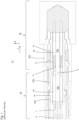
- the Figure 2 shows a schematic sectional drawing of a connector system 100 according to a preferred embodiment of the present invention.
- the conventional connector system 10 shown was used in the connector system 100 Figure 2 in particular the contact elements of the two connectors of the connector system are modified in order to improve the electrical properties and/or the signal transmission properties of the connectors or the connector system.
- the connector system 100 also includes the Figure 2 a connector plug 50a and a connector socket 50b.
- the connector plug 50a includes a plug housing 20a and two plug contact elements 13a, which are embedded in an insulator 18a of the connector plug 50a.
- the connector socket 50b includes a socket housing 20b and two plug contact elements 13b, which are embedded in an insulator 18b of the connector socket 13b.
- contact pins 5 of the plug contact elements 13a are in sockets 6 of the sockets along an insertion direction which corresponds to a longitudinal direction L of the plug connector system 100 or the plug connectors 50a and 50b.
- Contact elements 13b inserted.
- a cable 8 or an electrical conductor 7 of the cable 8 is soldered to each plug contact element 13a.
- the connector socket 13b can be connected to a circuit board (in the Figure 2 not visible).
- the arrow labeled L indicates a longitudinal direction or longitudinal axis of the connector system 100 or the connectors 50a and 50b, and the arrow labeled R indicates a radial direction of the connector system 100 or the connectors 50a and 50b .
- the contact elements 13a of the plug connector 50a point along the longitudinal axis L in contrast to the contact elements 4a of the conventional plug connector 1a Figure 1 corresponding to the contour or the contour jumps 14 of the connector housing 20a of the connector plug 50a has a reproduced contour or corresponding contour jumps 16.
- the contact elements 13b of the plug connector 50b also point along the longitudinal axis L in contrast to the contact elements 4b of the conventional plug connector 1b Figure 1 corresponding to the contour or the contour jumps 14 of the plug connector housing 20b of the plug connector socket 50b a simulated contour or corresponding contour jumps 16.
- the contour jumps 14 and 16 occur essentially in the radial direction R.
- the insulator 18a with the embedded contact element ducks 13a is arranged in the plug connector housing 20a in such a way that the contour jumps 14 of the plug connector housing 20a and the corresponding contour jumps 16 of the contact elements 13a lie one above the other essentially with respect to the longitudinal axis L of the plug connector 50a (or essentially the same axial position exhibit).
- the insulator 18b with the embedded contact element ducks 13b is arranged in the connector housing 20b in such a way that the contour jumps 14 of the plug connector housing 20b and the corresponding contour jumps 16 of the contact elements 13b lie one above the other (or essentially the same) with respect to the longitudinal axis L of the plug connector 50b have axial position).
- each of the contact elements 13a has a contact pin 5 in the form of a tapered end section.
- the contact elements 13a of the plug connector 50a are arranged and/or embedded in the insulator 18a in such a way that contour transitions or contour jumps 11 of the contact elements 13a to the respective tapered end section are arranged outside the insulator 18a or in the air gap 9.
- the contour transitions 11 of the plug contact elements 13a to the respective tapered end section are thus arranged between the insulator 18a of the plug connector plug 50a and the insulator 18b of the plug connector socket 50b.
- each of the contact elements 13a has a solder connection 15 for soldering an electrical conductor 7.
- the solder connections 15 are of Figure 1 designed as a widened cylindrical end section with a flattened side or a flattened side surface S (see also Figures 4a and 4b).
- the cables 8 to be soldered can thus be brought to the contact elements 13a essentially parallel, ie without a change in direction or without a bend and/or a kink, and soldered to the solder connection 15.
- the electrical properties or the signal transmission properties of the plug connector 13a, and thus also of the entire plug connector system 100 can be improved.
- FIG. 3 shows an enlarged section of the sectional drawing of the connector system 100 from Figure 2 .
- the contour or the contour jumps 16 of the contact elements 13a and 13b can be seen somewhat more clearly in this enlarged section.
- the vertical dashed line shown shows contour jumps 14 of the plug connector housing 20b and corresponding contour jumps 16 of the contact elements 13b at an axial position of the plug connector 50b.
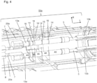
- the Figure 4 shows a perspective sectional drawing of a section of the connector system 100, in particular the connector plug 50a, from Figure 2 .
- the contact elements 13a each have different radii along the longitudinal axis L.
- the contour jumps 14 of the plug connector housing 20a and the corresponding contour jumps 16 of the contact elements 13a lie essentially one above the other with respect to the longitudinal axis L of the plug connector plug 50a.
- the contour jumps 14 of the plug connector housing 20a and the corresponding contour jumps 16 of the contact elements 13a therefore occur essentially at the same axial position of the plug connector plug 50a.
- each contact element 13a has the Figure 4 a plurality of first axial sections A1 with a first contact element radius and a plurality of second axial sections with a second contact element radius that differs from the first contact element radius or is smaller than the first contact element radius.
- the connector housing 20a has a plurality of first axial sections with a first inner connector housing radius and a plurality of second axial sections with a second inner connector housing radius that is different from the first inner connector housing radius or is smaller than the first inner connector housing radius. on.
- Each contact element 13a is arranged in the connector housing 20a in such a way that the first axial sections A1 of the contact element 13a and the corresponding first axial sections of the connector housing 20a essentially lie one above the other or are arranged essentially at the same axial positions of the connector plug 50a. Furthermore, each contact element 13a is arranged in the connector housing 20a in such a way that the second axial sections A2 of the contact element 13a and the corresponding second axial sections of the connector housing 20a essentially lie one above the other or are arranged essentially at the same axial positions of the connector plug 50a.
- each contact element 13a is arranged in the connector housing 20a in such a way that transitions between a first axial section A1 and a second axial section A2 of the respective contact element 13a occur essentially at those axial positions of the connector or connector plug 50a at which the connector housing 20a a contour change or a Has contour jump 14. Such transitions are in the Figure 4 marked by a dashed line.
- the Figure 5a shows a schematic drawing of a portion of the connector 50a to illustrate the connection of two cables 8 to the solder terminals 15 of the connector 50a according to a preferred embodiment of the present invention. Furthermore, it shows Figure 5b a corresponding schematic drawing of a section of the connector 50a in a perspective front view. For reasons of clarity, in the Figure 5b the electrical conductors 7 or cables 8 are not shown.
- the solder connections 15 are each designed as a widened cylindrical end section, which has a flattened (in particular milled) side. An electrical conductor 7 of the cable 8 is inserted into the flattened side of the widened end section and is connected to a flat surface F1 (see Figure 5b ) soldered on.
- the widened end sections of the contact elements 13a are flattened in such a way that they each have two flat surfaces F1 and F2 arranged orthogonally to one another.
- the surfaces F1 and F2 are arranged in such a way that together they form an L-shaped cross section.
- the contact elements 13a are arranged such that the respective flattened sides of the widened end portions of the contact elements 13a face each other.
- the widened end sections of the contact elements 13a are flattened (in particular milled) such that a distance d between a flat surface F1 of a first of the two contact elements 13a and a flat surface F1 of a second of the two contact elements 13a essentially corresponds to a predefined distance, which is on the diameter of the cable 8 to be soldered is matched.
- the cables 8 to be soldered can thus be Essentially parallel, ie without a change in direction or without a bend and/or a kink, are brought to the contact elements 13a and soldered to the solder connection 15.
- the electrical properties or the signal transmission properties of the plug connector 13a, and thus also of the entire plug connector system 100 can be improved.
Landscapes
- Engineering & Computer Science (AREA)
- Manufacturing & Machinery (AREA)
- Connector Housings Or Holding Contact Members (AREA)
- Coupling Device And Connection With Printed Circuit (AREA)
Applications Claiming Priority (1)
| Application Number | Priority Date | Filing Date | Title |
|---|---|---|---|
| DE102022202847.3A DE102022202847A1 (de) | 2022-03-23 | 2022-03-23 | Steckverbinder, Steckverbinder-System und Verfahren zum Herstellen des Steckverbinders |
Publications (1)
| Publication Number | Publication Date |
|---|---|
| EP4280384A1 true EP4280384A1 (fr) | 2023-11-22 |
Family
ID=85724869
Family Applications (1)
| Application Number | Title | Priority Date | Filing Date |
|---|---|---|---|
| EP23163397.5A Pending EP4280384A1 (fr) | 2022-03-23 | 2023-03-22 | Connecteur enfichable, système de connecteur enfichable et procédé de fabrication du connecteur enfichable ou du connecteur enfichable. système de connecteur |
Country Status (2)
| Country | Link |
|---|---|
| EP (1) | EP4280384A1 (fr) |
| DE (1) | DE102022202847A1 (fr) |
Citations (2)
| Publication number | Priority date | Publication date | Assignee | Title |
|---|---|---|---|---|
| US20130178106A1 (en) * | 2012-01-05 | 2013-07-11 | Ant Precision Industry Co., Ltd. | Receptacle connector and assembling method thereof |
| US20140378010A1 (en) * | 2012-02-11 | 2014-12-25 | Amphenol Tuchel Electronics Gmbh | Electrical plug connector for electrical connection by means of ultrasonic welding |
Family Cites Families (3)
| Publication number | Priority date | Publication date | Assignee | Title |
|---|---|---|---|---|
| FR54928E (fr) | 1946-08-16 | 1951-04-30 | Bendix Aviat Corp | Perfectionnements aux dispositifs électriques de connexion |
| US4957456A (en) | 1989-09-29 | 1990-09-18 | Hughes Aircraft Company | Self-aligning RF push-on connector |
| EP3930111A1 (fr) | 2020-06-24 | 2021-12-29 | Rosenberger Hochfrequenztechnik GmbH & Co. KG | Connecteur enfichable électrique et agencement de raccordement électrique |
-
2022
- 2022-03-23 DE DE102022202847.3A patent/DE102022202847A1/de active Pending
-
2023
- 2023-03-22 EP EP23163397.5A patent/EP4280384A1/fr active Pending
Patent Citations (2)
| Publication number | Priority date | Publication date | Assignee | Title |
|---|---|---|---|---|
| US20130178106A1 (en) * | 2012-01-05 | 2013-07-11 | Ant Precision Industry Co., Ltd. | Receptacle connector and assembling method thereof |
| US20140378010A1 (en) * | 2012-02-11 | 2014-12-25 | Amphenol Tuchel Electronics Gmbh | Electrical plug connector for electrical connection by means of ultrasonic welding |
Also Published As
| Publication number | Publication date |
|---|---|
| DE102022202847A1 (de) | 2023-09-28 |
Similar Documents
| Publication | Publication Date | Title |
|---|---|---|
| DE68924032T2 (de) | Federnd gestützter, selbsttragender, kontaktstiftaufnehmender elektrischer Doppelbalkenkontakt. | |
| DE3889841T2 (de) | Isolierungsverstellanordnung. | |
| EP3044833A1 (fr) | Connecteur enfichable | |
| DE112009000600T5 (de) | Bandmaterial, Verfahren zum Herstellen eines Innenleiteranschlusses und Koaxialverbinder | |
| DE69800778T2 (de) | Schneidklemmkontakt | |
| EP3627635A1 (fr) | Élément raccord, raccord pour modules, dispositif de carte de circuits imprimés et procédé de fabrication d'un élément raccord | |
| EP4295448B1 (fr) | Élément contact de conducteur intérieur pour connecteur à fiches coudé et procédé de fabrication associé | |
| DE69413734T2 (de) | Verfahren zum Verbinden von elektrischen Drähten | |
| EP3375047B1 (fr) | Contact à insérer et méthode de fabrication d'un contact à insérer | |
| EP0968548B1 (fr) | Douille munie de zones de contact a configuration hyperboloidale | |
| EP0578118B1 (fr) | Elément de contact à fiche | |
| EP4280384A1 (fr) | Connecteur enfichable, système de connecteur enfichable et procédé de fabrication du connecteur enfichable ou du connecteur enfichable. système de connecteur | |
| EP4250498A1 (fr) | Élément de contact, système d'élément de contact et connecteur enfichable | |
| DE29712306U1 (de) | Verlöt- oder Verschweissbarer Kabelverbinder | |
| EP0373709B1 (fr) | Appareil pour le raccordement d'un câble coaxial | |
| EP4216366A1 (fr) | Ligne de données pour un véhicule | |
| EP4250491B1 (fr) | Système d'élément de contact et connecteur enfichable | |
| EP4053862A1 (fr) | Élément de contact, composant smd et procédé de fabrication d'un tel composant smd | |
| DE102006020045B4 (de) | Zwischenstecker und Verfahren zur Herstellung eines Zwischensteckers | |
| DE102019104400A1 (de) | Einpresskontakt und Verfahren zum Herstellen des Einpresskontakts | |
| DE102017008065B4 (de) | Verbindersystem, Verbinderelement und Verfahren zur Herstellung eines Verbinderelements | |
| DE102022127543A1 (de) | Steckanordnung und Ethernet-Datensteckverbinder | |
| DE102017008087B4 (de) | Verbindersystem, Verbinderelement und Verfahren zur Herstellung eines Verbinderelements | |
| DE102024112717A1 (de) | Elektrisches Kabel oder elektrische Leitung ausgebildet mit einer kalibrierten Steckkontur zum direkten Einstecken in einen Gegenstecker | |
| DE102023132382A1 (de) | Kopplungsvorrichtung |
Legal Events
| Date | Code | Title | Description |
|---|---|---|---|
| PUAI | Public reference made under article 153(3) epc to a published international application that has entered the european phase |
Free format text: ORIGINAL CODE: 0009012 |
|
| STAA | Information on the status of an ep patent application or granted ep patent |
Free format text: STATUS: THE APPLICATION HAS BEEN PUBLISHED |
|
| AK | Designated contracting states |
Kind code of ref document: A1 Designated state(s): AL AT BE BG CH CY CZ DE DK EE ES FI FR GB GR HR HU IE IS IT LI LT LU LV MC ME MK MT NL NO PL PT RO RS SE SI SK SM TR |
|
| STAA | Information on the status of an ep patent application or granted ep patent |
Free format text: STATUS: REQUEST FOR EXAMINATION WAS MADE |
|
| 17P | Request for examination filed |
Effective date: 20240516 |
|
| RBV | Designated contracting states (corrected) |
Designated state(s): AL AT BE BG CH CY CZ DE DK EE ES FI FR GB GR HR HU IE IS IT LI LT LU LV MC ME MK MT NL NO PL PT RO RS SE SI SK SM TR |
|
| STAA | Information on the status of an ep patent application or granted ep patent |
Free format text: STATUS: EXAMINATION IS IN PROGRESS |
|
| 17Q | First examination report despatched |
Effective date: 20251210 |