EP4283660B1 - Direktes klebeverfahren mit unterstützung durch kationische elemente - Google Patents
Direktes klebeverfahren mit unterstützung durch kationische elemente Download PDFInfo
- Publication number
- EP4283660B1 EP4283660B1 EP23173765.1A EP23173765A EP4283660B1 EP 4283660 B1 EP4283660 B1 EP 4283660B1 EP 23173765 A EP23173765 A EP 23173765A EP 4283660 B1 EP4283660 B1 EP 4283660B1
- Authority
- EP
- European Patent Office
- Prior art keywords
- substrate
- bonding
- bonding surface
- manufacturing
- aqueous solution
- Prior art date
- Legal status (The legal status is an assumption and is not a legal conclusion. Google has not performed a legal analysis and makes no representation as to the accuracy of the status listed.)
- Active
Links
Images
Classifications
-
- H—ELECTRICITY
- H10—SEMICONDUCTOR DEVICES; ELECTRIC SOLID-STATE DEVICES NOT OTHERWISE PROVIDED FOR
- H10P—GENERIC PROCESSES OR APPARATUS FOR THE MANUFACTURE OR TREATMENT OF DEVICES COVERED BY CLASS H10
- H10P90/00—Preparation of wafers not covered by a single main group of this subclass, e.g. wafer reinforcement
-
- H—ELECTRICITY
- H10—SEMICONDUCTOR DEVICES; ELECTRIC SOLID-STATE DEVICES NOT OTHERWISE PROVIDED FOR
- H10W—GENERIC PACKAGES, INTERCONNECTIONS, CONNECTORS OR OTHER CONSTRUCTIONAL DETAILS OF DEVICES COVERED BY CLASS H10
- H10W70/00—Package substrates; Interposers; Redistribution layers [RDL]
- H10W70/01—Manufacture or treatment
- H10W70/05—Manufacture or treatment of insulating or insulated package substrates, or of interposers, or of redistribution layers
- H10W70/093—Connecting or disconnecting other interconnections thereto or therefrom, e.g. connecting bond wires or bumps
-
- H—ELECTRICITY
- H10—SEMICONDUCTOR DEVICES; ELECTRIC SOLID-STATE DEVICES NOT OTHERWISE PROVIDED FOR
- H10W—GENERIC PACKAGES, INTERCONNECTIONS, CONNECTORS OR OTHER CONSTRUCTIONAL DETAILS OF DEVICES COVERED BY CLASS H10
- H10W10/00—Isolation regions in semiconductor bodies between components of integrated devices
- H10W10/10—Isolation regions comprising dielectric materials
-
- H—ELECTRICITY
- H10—SEMICONDUCTOR DEVICES; ELECTRIC SOLID-STATE DEVICES NOT OTHERWISE PROVIDED FOR
- H10P—GENERIC PROCESSES OR APPARATUS FOR THE MANUFACTURE OR TREATMENT OF DEVICES COVERED BY CLASS H10
- H10P70/00—Cleaning of wafers, substrates or parts of devices
- H10P70/20—Cleaning during device manufacture
- H10P70/23—Cleaning during device manufacture during, before or after processing of insulating materials
-
- H—ELECTRICITY
- H10—SEMICONDUCTOR DEVICES; ELECTRIC SOLID-STATE DEVICES NOT OTHERWISE PROVIDED FOR
- H10P—GENERIC PROCESSES OR APPARATUS FOR THE MANUFACTURE OR TREATMENT OF DEVICES COVERED BY CLASS H10
- H10P90/00—Preparation of wafers not covered by a single main group of this subclass, e.g. wafer reinforcement
- H10P90/19—Preparing inhomogeneous wafers
- H10P90/1904—Preparing vertically inhomogeneous wafers
- H10P90/1906—Preparing SOI wafers
- H10P90/1914—Preparing SOI wafers using bonding
-
- H—ELECTRICITY
- H10—SEMICONDUCTOR DEVICES; ELECTRIC SOLID-STATE DEVICES NOT OTHERWISE PROVIDED FOR
- H10P—GENERIC PROCESSES OR APPARATUS FOR THE MANUFACTURE OR TREATMENT OF DEVICES COVERED BY CLASS H10
- H10P95/00—Generic processes or apparatus for manufacture or treatments not covered by the other groups of this subclass
- H10P95/90—Thermal treatments, e.g. annealing or sintering
-
- H—ELECTRICITY
- H10—SEMICONDUCTOR DEVICES; ELECTRIC SOLID-STATE DEVICES NOT OTHERWISE PROVIDED FOR
- H10W—GENERIC PACKAGES, INTERCONNECTIONS, CONNECTORS OR OTHER CONSTRUCTIONAL DETAILS OF DEVICES COVERED BY CLASS H10
- H10W10/00—Isolation regions in semiconductor bodies between components of integrated devices
- H10W10/01—Manufacture or treatment
- H10W10/011—Manufacture or treatment of isolation regions comprising dielectric materials
-
- H—ELECTRICITY
- H10—SEMICONDUCTOR DEVICES; ELECTRIC SOLID-STATE DEVICES NOT OTHERWISE PROVIDED FOR
- H10W—GENERIC PACKAGES, INTERCONNECTIONS, CONNECTORS OR OTHER CONSTRUCTIONAL DETAILS OF DEVICES COVERED BY CLASS H10
- H10W10/00—Isolation regions in semiconductor bodies between components of integrated devices
- H10W10/10—Isolation regions comprising dielectric materials
- H10W10/181—Semiconductor-on-insulator [SOI] isolation regions, e.g. buried oxide regions of SOI wafers
Definitions
- the present invention relates to the field of direct bonding. It relates in particular to a method of manufacturing a multilayer structure by direct bonding.
- Direct bonding is a technique now well known and used for industrial applications such as the manufacturing of SOI by SOITEC or STMicroelectronics for the production of imagers for example.
- direct bonding is a spontaneous bonding between two surfaces without adding material to the interface between the bonded surfaces, and in particular without a thick layer of liquid. It is nevertheless possible to have some monolayers of water adsorbed on the surfaces, which represents between 0.25 nm and 1.25 nm of thickness, so that these surfaces are macroscopically dry.
- Direct bonding is typically performed at room temperature and ambient pressure, but this is not a requirement.
- An important characteristic of direct bonding is its adhesion energy, i.e. the energy available to achieve spontaneous bonding. This is the energy that allows the two surfaces to be deformed to bring them into contact at the atomic scale so that the Van der Waals forces can be implemented.
- the adhesion energy typically ranges from 30 to 100 mJ/m 2 . This adhesion energy partly directs the duration of the propagation of the bonding wave, for example the bonding wave typically propagates in 9 seconds for the direct bonding of two 200 mm silicon substrates.
- Another important characteristic of direct bonding is its adhesion energy or otherwise called its bonding energy. This is the energy that must be used to separate the two bonded surfaces. For example, for two hydrophilic silicon or silicon oxide surfaces, the adhesion energy typically ranges from 0.14 J/m 2 to 6 J/m 2 .
- the surfaces are generally cleaned of organic and particulate contaminations which are very detrimental to direct bonding.
- cleaning is carried out beforehand on the surfaces to be bonded with a solution based on Caro acid obtained with a mixture of 96% sulfuric acid and 30% hydrogen peroxide (3:1) at 180°C and SCI (mixture of 30% ammonia, 30% hydrogen peroxide and deionized water (1:1:5)) at 70°C.
- SCI mixture of 30% ammonia, 30% hydrogen peroxide and deionized water (1:1:5)
- it is possible to use other highly oxidizing cleaning solutions such as, for example, aqueous solutions containing ozone or with a treatment using exposure to UV light in the presence of gaseous ozone.
- the adhesion energy of a SiO 2 -SiO 2 bond (two silicon substrates covered with approximately 145 nm thermal oxide for example), in a clean room environment, with chemical cleaning based on Caro and SCI at 70°C, is worth approximately 140mJ/ m2 just after bonding, without heat treatment.
- the bonding energy also changes depending on the heat treatment applied after bonding at room temperature.
- the adhesion energy increases depending on the temperature of the heat treatments.
- the SiO 2 -SiO 2 bonding energy increases slowly to reach, depending on the surface treatment, almost 3J/m 2 at 500°C and then stagnates up to 800°C.
- plasma treatment also modifies the surface over a thickness of a few nanometers (between 1 and 10 nm). This modification can disrupt future devices.
- the plasma creates an oxide layer that is difficult to control in terms of thickness and quality.
- certain plasmas such as N2 plasma create interfacial charge problems that can disrupt the electrical operation of future devices.
- This direct bonding process thus carried out makes it possible to obtain a multilayer structure having a bonding energy greater than that of a multilayer structure obtained by a direct bonding process devoid of step c) of treatment in a cationic aqueous solution.
- a high bonding energy is then obtained at low temperature, i.e. at temperatures below 400°C, preferably less than or equal to 350°C and more preferably a temperature of 200°C.
- bonding temperatures are compatible with many applications and/or with many substrates, whose nature and/or presence of electronic and/or optoelectronic components require low thermal budgets.
- the process is applicable to many materials and is inexpensive.
- the process leads to multilayer structures with good mechanical strength after bonding, compatible with subsequent processes such as Smart Cut TM and/or any process generating mechanical stresses on the assembly, such as mechanical thinning.
- this process does not affect the adhesion energy since the use of a cationic aqueous solution is only carried out after the surfaces have come into direct contact.
- the bonding wave always propagates in 9 seconds for silicon substrates of approximately 200 mm.
- Post-bonding heat treatment is also known to those skilled in the art as 'bonding annealing'.
- the heat treatment according to step d) is carried out by a temperature increase, from ambient temperature to a final temperature, the temperature increase being carried out over a period of a few hours, for example 2 hours for a final temperature of 300°C.
- the temperature of the heat treatment applied in step d) is between 100°C and 300°C, in particular between 150°C and 250°C.
- step c) of arranging the direct bonding interface in the cationic aqueous solution is carried out for a period of approximately 5 min to 40 days.
- step c The duration of this step increases with the diameter of the first and second substrates. It is indeed necessary that the cationic species have time to move over the entire direct bonding interface to obtain a homogeneous and uniform bonding energy. Also, the larger the diameter of the multilayer structure, the longer the duration of step c).
- step c) consists in immersing at least the direct bonding interface in said cationic aqueous solution.
- the multilayer assembly obtained in step b) is totally or partially immersed in the cationic aqueous solution to the extent that the direct bonding interface is immersed in said cationic aqueous solution.
- the first bonding surface and/or the second bonding surface is formed at least in part by a hydrophilic film of a material selected from a native oxide, a thermal or deposited silicon oxide, a silicon nitride, a copper oxide and a combination of these materials.
- the hydrophilic copper oxide film is a hybrid film composed of copper pads separated by SiO2. The copper pads are almost instantly covered in air with a native copper oxide.
- the hydrophilic film is made of oxide, it is for example formed by a deposited oxide, a thin oxide film obtained by a heat treatment (also called thermal oxide) and/or a thin oxide film obtained by a chemical treatment (also called native oxide or chemical oxide).
- the first and/or second substrate are made of oxidized material(s), such as alumina, such that the first bonding surface and/or the second bonding surface are formed by the material of the first and/or second substrate respectively because it is an intrinsically hydrophilic material. This does not prohibit the presence of a hydrophilic film in addition.
- the first bonding surface is hydrophobic (for example made of hydrophobic silicon obtained by passivation of the silicon surface and grafting of hydrogen onto the silicon) and the second bonding surface is hydrophilic.
- the second bonding surface is formed at least in part by a hydrophilic film chosen from a native oxide (silicon, Ge, ... depending on the material of the second substrate), a thermal oxide (silicon), a deposited oxide, a silicon nitride, a copper oxide and a combination of these compounds, or the second bonding surface is constituted by the material of the second substrate which is an oxide and therefore hydrophilic. Bringing the second hydrophilic surface into contact with the hydrophobic surface changes the initial hydrophobic character of the latter into a hydrophilic character which allows direct bonding.
- the first bonding surface and the second bonding surface are completely planar. That is, the first and second bonding surfaces are free of recesses or microscopically plateau-forming patterns.
- the first bonding surface and/or the second bonding surface are cleaned by treatment with ozonated water and/or treatment SC1 and/or treatment SC2 before step b).
- the first substrate and the second substrate have a diameter strictly greater than 2.5 cm.
- step a) further comprises drying the first bonding surface and the second bonding surface before carrying out step b) of bringing into contact.
- the first bonding surface and the second bonding surface each have a face on which resides at most one to five monoatomic layers of H 2 O, such that the first bonding surface and the second bonding surface are dry on a macroscopic scale.
- the cationic aqueous solution comprises cationic species selected from Na + , Mg2 + , Ca2 + , K + , Ba2 + and a mixture of these cationic species.
- the cationic aqueous solution is formed, by dissolving in deionized water, a salt chosen from NaCl, MgCl 2 , CaCl 2 , KCl, BaCl 2 , NaF, KCI, KF and a mixture of these compounds.
- the cationic aqueous solution has a mass concentration of cationic species between 10 -8 g/ml and 0.5 g/ml, in particular between 10 -8 g/ml and 10 -2 g/ml and in particular between 10 -8 g/ml and 10 -4 g/ml.
- a low concentration of cations is sufficient to ensure strong bonding which allows a low-cost step.
- a higher concentration leads to poorer results.
- the first substrate and the second substrate are each formed by a material selected from semiconductor materials, such as silicon, silicon oxides, silicon nitrides, SiOC, alumina, diamond, and a combination of these materials, or even LNO (acronym for lanthanum nickel oxide LaNiO3), LTO (acronym for lithium titanate Li2TiO3), germanium, germanium oxide, SiC, InP, AsGa, GaN and a combination of these materials.
- semiconductor materials such as silicon, silicon oxides, silicon nitrides, SiOC, alumina, diamond, and a combination of these materials, or even LNO (acronym for lanthanum nickel oxide LaNiO3), LTO (acronym for lithium titanate Li2TiO3), germanium, germanium oxide, SiC, InP, AsGa, GaN and a combination of these materials.
- semiconductor materials such as silicon, silicon oxides, silicon nitrides, SiOC, alumina, diamond, and a combination of
- the first substrate and the second substrate may be of the same nature or of different nature.
- the bonding energy is measured for example with the double lever method with imposed displacement in an anhydrous atmosphere as described in the article by F. Fournel, L. Continni, C. Morales, J. Da Fonseca, H. Moriceau, F. Rieutord, A. Barthelemy, and I. Radu, Journal of Applied Physics 111, 104907 (2012 ).
- the first substrate provided in step a) comprises one or more first vignettes originating from the vignetting of the first substrate so as to obtain direct bonding of one or more first vignettes to the second substrate.
- the first bonding surface is delimited by the exposed face of one or more first vignettes.
- the second substrate provided in step a) comprises one or more second vignettes originating from the vignetting of the second substrate so as to obtain a direct bonding between one or more first vignettes and one or more second vignettes.
- the second bonding surface is delimited by the exposed face of one or more second vignettes.
- the method of the present invention provides a direct bonding method between a first and a second substrate 1,2 comprising an immersion step c) in a cationic aqueous solution followed by a bonding annealing step d) at low temperature which makes it possible to achieve a high bonding energy.
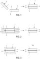
- a first substrate 1 and a second substrate 2, both made of silicon and each having a completely flat bonding surface 3,4 over a diameter of 200 mm, are provided according to step a) of the method.
- the first bonding surface 3 and the second bonding surface 4 are formed by a hydrophilic film 5 of silicon oxide (thermal or deposited) of approximately 145 nm thickness.
- the method comprises cleaning with ozonated water the two bonding surfaces 3, 4 and/or an SC1 treatment (mixture of 30% ammonia, 30% hydrogen peroxide and deionized water in the respective volume proportions 1:1:5) and/or an SC2 treatment (mixture of 30% hydrochloric acid, 30% hydrogen peroxide and water in the respective volume proportions 1:1:5) so as to remove organic and particulate contaminants which are very detrimental to direct bonding.
- the two surfaces 3 and 4 are then brought into contact so as to create a direct bonding interface 6 between the two substrates 1, 2. According to a non-visible possibility, only one of the two bonding surfaces 3, 4 is formed by a silicon oxide film 5.
- a step of preparing the first and second bonding surfaces 3, 4 before the contacting of step b) comprises a plasma treatment.
- the first and second bonding surfaces 3, 4 are dried before the contacting step b), so as to remove the water present on a macroscopic scale, for example by centrifugation at 2000 rpm to obtain spontaneous direct bonding.
- a cationic aqueous solution 8 is then prepared by dissolving NaCl in deionized water until a concentration of 10 -4 g/ml of cationic species is reached.
- the direct bonding interface 6 (here the entire assembly 7 obtained in step b) is then immersed in this solution 8 according to step c) of the method. The immersion is carried out for a period of approximately 20 days so that the cationic species have time to migrate over the entire direct bonding interface 6. This period is shorter when the substrates 1, 2 have a smaller diameter.
- the first substrate and/or the second substrate 1, 2 comprise recesses opening respectively at the first and/or the second surface of 3, 4, creating cavities at the direct bonding interface 6. The migration of the cationic species to the bonding interface 6 is then faster in this case and the duration of the immersion in the cationic aqueous solution 8 can be reduced.
- a bonding anneal is carried out on the assembly 7 until a temperature of 300°C is reached according to step d) of the process ( figure 3 ).
- the measurement of the bonding energy (double lever method) carried out on the multilayer structure 100 thus obtained leads to the breakage of the silicon substrates 1,2 and not to the detachment of the substrates 1,2 at the direct bonding interface 6. This indicates that the bonding energy reached is greater than the fracture energy of the silicon, i.e. a bonding energy greater than 5J/m2.
- the same process carried out without step c) of immersion in a cationic aqueous solution 8 leads to a bonding energy of 3J/m2 measured according to the same double lever method, after a bonding anneal at 500°C.
- one of the two substrates 1,2 provided in step a) has a weakening plane.
- the bonding annealing heat treatment contributes to the thermal budget allowing a fracture at the weakening plane.
- the multilayer structure 100 obtained then comprises one of the two substrates 1,2 bonded to a transferred thin layer originating from the fracture and a negative of the other of the substrates 1,2.
- the first substrate 1 provided in step a) is vignetted into several first vignettes whose exposed faces are first bonding surfaces 3.
- the first vignettes are bonded according to the method previously described on the second substrate 2 (full wafer) according to a chip-wafer bonding also known in English terminology by the expression 'chip to wafer'.
- the second substrate 2 is also vignetted into several second vignettes and the method of the invention allows the direct bonding of the first vignettes and the second vignettes.
- first bonding surface 3 and the second bonding surface 4 are prepared so as to have copper-oxide hybrid surfaces that can be bonded in direct bonding.
- These first and second hydrophilic bonding surfaces 3, 4 are typically composed of copper pads with a side of 2.5 micrometers separated by 2.5 micrometers of SiO2. This is then referred to as a hybrid surface with a “pitch” of 5 micrometers. Then steps b) to d) of the method are reproduced as previously described.
- the present invention proposes a method for manufacturing a multilayer structure 100 comprising direct bonding between two substrates 1,2 having a high bonding energy, and making it possible to limit the temperature of the post-bonding thermal annealing.
- the cationic aqueous solution is inexpensive and the immersion step c) is applicable to many materials. It is in particular possible to bond substrates (or thick layers) of materials having a significant difference in thermal expansion coefficient.
- the materials of the first and second substrates 1,2 comprise devices, these are not damaged by the temperatures used.
Landscapes
- Pressure Welding/Diffusion-Bonding (AREA)
- Laminated Bodies (AREA)
Claims (10)
- Verfahren zur Herstellung einer Mehrschichtstruktur (100) durch direkte Verklebung zwischen einem ersten Substrat (1) und einem zweiten Substrat (2), wobei das Verfahren die Schritte umfasst zum:a) Bereitstellen eines ersten Substrats (1) und eines zweiten Substrats (2), die eine erste Klebefläche (3) beziehungsweise eine zweite Klebefläche (4) umfassen,b) In-Kontakt-Bringen der ersten Klebefläche (3) und der zweiten Klebefläche (4), so dass eine Grenzfläche der direkten Verklebung (6) zwischen dem ersten Substrat (1) und dem zweiten Substrat (2) geschaffen wird,c) Anordnen mindestens der Grenzfläche der direkten Verklebung (6) in einer kationischen wässrigen Lösung (8), die deionisiertes Wasser umfasst und kationische Spezies, die aus mindestens einem Element der ersten und/oder der zweiten Spalte des Periodensystems der Elemente hervorgegangen sind, undd) Anwenden einer Wärmebehandlung bei einer Temperatur zwischen 20 °C und 350 °C, so dass die Mehrschichtstruktur (100) erhalten wird.
- Herstellungsverfahren nach Anspruch 1, wobei der Schritt c) zur Anordnung der Grenzfläche der direkten Verklebung (6) in der kationischen wässrigen Lösung (8) über einen Zeitraum von etwa 5 min bis 45 Tagen durchgeführt wird.
- Herstellungsverfahren nach Anspruch 1 oder 2, wobei die erste Klebefläche (3) und/oder die zweite Klebefläche (4) mindestens teilweise durch einen hydrophilen Film (5) aus einem Material gebildet sind, das aus einem nativen Oxid, einem thermischen oder abgeschiedenen Siliciumoxid, einem Siliciumnitrid, einem Kupferoxid und einer Kombination dieser Materialien ausgewählt ist.
- Herstellungsverfahren nach einem der Ansprüche 1 bis 3, wobei die erste Klebefläche (3) und die zweite Klebefläche (4) vollständig eben sind.
- Herstellungsverfahren nach einem der Ansprüche 1 bis 4, wobei die erste Klebefläche (3) und/oder die zweite Klebefläche (4) durch eine Behandlung mit ozonisiertem Wasser und/oder SC1-Behandlung und/oder SC2-Behandlung vor dem Schritt b) gereinigt werden.
- Herstellungsverfahren nach einem der Ansprüche 1 bis 5, wobei die kationische wässrige Lösung (8) kationische Spezies umfasst, die aus Na+, Mg2+, Ca2+, K+, Ba2+ und einem Gemisch dieser kationischen Spezies ausgewählt sind.
- Herstellungsverfahren nach einem der Ansprüche 1 bis 6, wobei die kationische wässrige Lösung (8) durch Auflösen in deionisiertem Wasser eines Salzes gebildet wird, das aus NaCl, MgCl2, CaCl2, KCl, BaCl2, NaF, KCI, KF und einem Gemisch dieser Verbindungen ausgewählt ist.
- Herstellungsverfahren nach Anspruch 1 bis 7, wobei die kationische wässrige Lösung (8) eine Massenkonzentration der kationischen Spezies zwischen 10-8 g/ml und 0,5 g/ml aufweist, besonders zwischen 10-8 g/ml und 10-2 g/ml und insbesondere zwischen 10-8 g/ml und 10-4 g/ml.
- Herstellungsverfahren nach einem der Ansprüche 1 bis 8, wobei das erste Substrat (1) und das zweite Substrat (2) jeweils aus einem Material gebildet sind, das aus Halbleitermaterialien wie Si, Siliciumoxiden, Siliciumnitriden, SiOC, Aluminiumoxid, Diamant und einer Kombination dieser Materialien ausgewählt ist.
- Herstellungsverfahren nach einem der Ansprüche 1 bis 9, wobei:das erste Substrat (1) und das zweite Substrat (2), die in Schritt a) bereitgestellt werden, jeweils ein Siliciumsubstrat umfassen, das einen Durchmesser zwischen 100 mm und 250 mm aufweist, insbesondere 200 mm, und die erste Klebefläche (3) und die zweite Klebefläche (4) jeweils durch einen Siliciumoxidfilm (5) gebildet sind,der Schritt c) die Anordnung der Grenzfläche (6) der direkten Verklebung umfasst, die in Schritt b) erhalten wurde, in der kationischen wässrigen Lösung (8), über einen Zeitraum von 15 bis 20 Tagen, für erste und zweite Substrate von 200 mm, wobei die kationische wässrige Lösung (8) eine Lösung ist, die durch Auflösen von NaCl in deionisiertem Wasser gebildet wird, so dass eine Massenkonzentration zwischen 10-8 g/ml und 0.001 g/ml erreicht wird, und beispielsweise eine Massenkonzentration von etwa 10-4 g/ml, undder Schritt d) die Anwendung einer Wärmebehandlung bei etwa 300 °C umfasst, so dass eine direkte Verklebung zwischen dem ersten Substrat (1) und dem zweiten Substrat (2) erhalten wird, eine Verklebungsenergie von mehr als 5 J/m2 aufweisend.
Applications Claiming Priority (1)
| Application Number | Priority Date | Filing Date | Title |
|---|---|---|---|
| FR2205053A FR3136108B1 (fr) | 2022-05-25 | 2022-05-25 | Procédé de collage direct assisté par des élements cationiques |
Publications (2)
| Publication Number | Publication Date |
|---|---|
| EP4283660A1 EP4283660A1 (de) | 2023-11-29 |
| EP4283660B1 true EP4283660B1 (de) | 2024-11-20 |
Family
ID=82319908
Family Applications (1)
| Application Number | Title | Priority Date | Filing Date |
|---|---|---|---|
| EP23173765.1A Active EP4283660B1 (de) | 2022-05-25 | 2023-05-16 | Direktes klebeverfahren mit unterstützung durch kationische elemente |
Country Status (5)
| Country | Link |
|---|---|
| US (1) | US12532717B2 (de) |
| EP (1) | EP4283660B1 (de) |
| JP (1) | JP2023174560A (de) |
| CN (1) | CN117133668A (de) |
| FR (1) | FR3136108B1 (de) |
Families Citing this family (4)
| Publication number | Priority date | Publication date | Assignee | Title |
|---|---|---|---|---|
| FR3136106B1 (fr) * | 2022-05-25 | 2024-05-31 | Commissariat Energie Atomique | Procédé de collage direct assisté par une molécule basique |
| FR3136108B1 (fr) | 2022-05-25 | 2024-04-19 | Commissariat Energie Atomique | Procédé de collage direct assisté par des élements cationiques |
| US12532780B2 (en) * | 2022-08-22 | 2026-01-20 | Micron Technology, Inc. | Hybrid bonding for semiconductor device assemblies |
| CN219246703U (zh) * | 2022-12-06 | 2023-06-23 | 苏州晶湛半导体有限公司 | 一种复合衬底、外延片及半导体器件 |
Family Cites Families (13)
| Publication number | Priority date | Publication date | Assignee | Title |
|---|---|---|---|---|
| FR2868599B1 (fr) * | 2004-03-30 | 2006-07-07 | Soitec Silicon On Insulator | Traitement chimique optimise de type sc1 pour le nettoyage de plaquettes en materiau semiconducteur |
| US7919391B2 (en) | 2004-12-24 | 2011-04-05 | S.O.I.Tec Silicon On Insulator Technologies | Methods for preparing a bonding surface of a semiconductor wafer |
| FR2880186B1 (fr) * | 2004-12-24 | 2007-07-20 | Soitec Silicon On Insulator | Procede de traitement d'une surface de plaquette |
| FR2963158B1 (fr) * | 2010-07-21 | 2013-05-17 | Commissariat Energie Atomique | Procede d'assemblage par collage direct entre deux elements comprenant des portions de cuivre et de materiaux dielectriques |
| US20180095067A1 (en) * | 2015-04-03 | 2018-04-05 | Abbott Laboratories | Devices and methods for sample analysis |
| JP6486308B2 (ja) * | 2015-12-28 | 2019-03-20 | 富士フイルム株式会社 | ハードコートフィルムおよびその応用 |
| WO2017160961A1 (en) * | 2016-03-17 | 2017-09-21 | 3M Innovative Properties Company | Membrane assemblies, electrode assemblies, membrane-electrode assemblies and electrochemical cells and liquid flow batteries therefrom |
| US11629096B2 (en) * | 2017-11-20 | 2023-04-18 | Corning Incorporated | Temporary bonding of glass pairs using cationic surfactants and/or organic salts |
| WO2019202067A1 (en) * | 2018-04-20 | 2019-10-24 | Aveni | Method for temporary or permanent wafer bonding |
| WO2020032283A1 (ja) | 2018-08-09 | 2020-02-13 | 株式会社日本触媒 | 吸水性シートおよびそれを含む吸水性物品 |
| FR3102771B1 (fr) * | 2019-10-31 | 2021-10-08 | Commissariat Energie Atomique | Procédé de collage de deux surfaces hydrophiles |
| WO2023276638A1 (ja) | 2021-06-30 | 2023-01-05 | ダイキン工業株式会社 | 積層体の製造方法および積層体 |
| FR3136108B1 (fr) | 2022-05-25 | 2024-04-19 | Commissariat Energie Atomique | Procédé de collage direct assisté par des élements cationiques |
-
2022
- 2022-05-25 FR FR2205053A patent/FR3136108B1/fr active Active
-
2023
- 2023-05-12 US US18/316,338 patent/US12532717B2/en active Active
- 2023-05-16 EP EP23173765.1A patent/EP4283660B1/de active Active
- 2023-05-16 JP JP2023080555A patent/JP2023174560A/ja active Pending
- 2023-05-24 CN CN202310593951.3A patent/CN117133668A/zh active Pending
Also Published As
| Publication number | Publication date |
|---|---|
| JP2023174560A (ja) | 2023-12-07 |
| FR3136108A1 (fr) | 2023-12-01 |
| EP4283660A1 (de) | 2023-11-29 |
| CN117133668A (zh) | 2023-11-28 |
| FR3136108B1 (fr) | 2024-04-19 |
| US12532717B2 (en) | 2026-01-20 |
| US20230386891A1 (en) | 2023-11-30 |
Similar Documents
| Publication | Publication Date | Title |
|---|---|---|
| EP4283660B1 (de) | Direktes klebeverfahren mit unterstützung durch kationische elemente | |
| EP1879220A2 (de) | Direktes hydrophobes Verfahren zum Kleben von zwei Substraten zur Verwendung in der Elektronik, Optik und Opto-Elektronik. | |
| FR2797347A1 (fr) | Procede de transfert d'une couche mince comportant une etape de surfragililisation | |
| EP2842155B1 (de) | Bindungsverfahren in der atmosphäre eines gases mit einem negativen joule-thomson-koeffizienten | |
| FR2744285A1 (fr) | Procede de transfert d'une couche mince d'un substrat initial sur un substrat final | |
| EP4283658B1 (de) | Verfahren zum direkten bonden mit hilfe eines basischen moleküls | |
| EP4283659B1 (de) | Verfahren zum direkt-bonden, mit hilfe starker basen | |
| EP3425657B1 (de) | Verfahren zur herstellung einer schnittstelle für die temporäre montage eines mikroelektronischen supports und eines bedienungsgriffs, und entsprechende temporäre montageschnittstelle | |
| EP3260511B1 (de) | Reversibles klebeverfahren zwischen zwei elementen | |
| FR2888402A1 (fr) | Procede d'assemblage de substrats par depot d'une couche mince de collage d'oxyde ou de nitrure et structure ainsi assemblee | |
| WO2020188169A1 (fr) | Procede de transfert d'une couche utile sur une substrat support | |
| EP2676288B1 (de) | Verfahren zur herstellung einer substrathalterung | |
| EP4088309B1 (de) | Verfahren zum verbinden zweier halbleitersubstrate | |
| FR2880186A1 (fr) | Procede de traitement d'une surface de plaquette | |
| EP3721467B1 (de) | Verfahren zur herstellung des restes eines donorsubstrats, nach diesem verfahren hergestelltes substrat und verwendung eines solchen substrats | |
| EP4453997A1 (de) | Verfahren zur herstellung zerlegbarer substrate | |
| EP3961684A1 (de) | Verfahren zur herstellung eines substrats zum temporären verkleben eines substrats | |
| WO2020188168A1 (fr) | Procede de transfert d'une couche utile sur un substrat support | |
| WO2002076881A1 (fr) | Procede de fabrication d'une structure a membrane micro-usinee | |
| FR3059149A1 (fr) | Procede de fabrication d'un film mince a base d'inp ou de gaas | |
| FR2880185A1 (fr) | Procede de traitement d'une surface de plaquette |
Legal Events
| Date | Code | Title | Description |
|---|---|---|---|
| PUAI | Public reference made under article 153(3) epc to a published international application that has entered the european phase |
Free format text: ORIGINAL CODE: 0009012 |
|
| STAA | Information on the status of an ep patent application or granted ep patent |
Free format text: STATUS: REQUEST FOR EXAMINATION WAS MADE |
|
| 17P | Request for examination filed |
Effective date: 20230516 |
|
| AK | Designated contracting states |
Kind code of ref document: A1 Designated state(s): AL AT BE BG CH CY CZ DE DK EE ES FI FR GB GR HR HU IE IS IT LI LT LU LV MC ME MK MT NL NO PL PT RO RS SE SI SK SM TR |
|
| GRAP | Despatch of communication of intention to grant a patent |
Free format text: ORIGINAL CODE: EPIDOSNIGR1 |
|
| STAA | Information on the status of an ep patent application or granted ep patent |
Free format text: STATUS: GRANT OF PATENT IS INTENDED |
|
| RIC1 | Information provided on ipc code assigned before grant |
Ipc: H01L 21/762 20060101ALN20240808BHEP Ipc: H01L 21/20 20060101ALN20240808BHEP Ipc: H01L 21/02 20060101ALI20240808BHEP Ipc: H01L 21/18 20060101AFI20240808BHEP |
|
| RIN1 | Information on inventor provided before grant (corrected) |
Inventor name: MORALES, CHRISTOPHE Inventor name: LARREY, VINCENT Inventor name: CALVEZ, AZILIZ Inventor name: FOURNEL, FRANK |
|
| INTG | Intention to grant announced |
Effective date: 20240829 |
|
| RAP3 | Party data changed (applicant data changed or rights of an application transferred) |
Owner name: COMMISSARIAT A L'ENERGIE ATOMIQUE ET AUX ENERGIESALTERNATIVES |
|
| GRAS | Grant fee paid |
Free format text: ORIGINAL CODE: EPIDOSNIGR3 |
|
| GRAA | (expected) grant |
Free format text: ORIGINAL CODE: 0009210 |
|
| STAA | Information on the status of an ep patent application or granted ep patent |
Free format text: STATUS: THE PATENT HAS BEEN GRANTED |
|
| RAP3 | Party data changed (applicant data changed or rights of an application transferred) |
Owner name: COMMISSARIAT A L'ENERGIE ATOMIQUE ET AUX ENERGIESALTERNATIVES |
|
| AK | Designated contracting states |
Kind code of ref document: B1 Designated state(s): AL AT BE BG CH CY CZ DE DK EE ES FI FR GB GR HR HU IE IS IT LI LT LU LV MC ME MK MT NL NO PL PT RO RS SE SI SK SM TR |
|
| REG | Reference to a national code |
Ref country code: GB Ref legal event code: FG4D Free format text: NOT ENGLISH |
|
| REG | Reference to a national code |
Ref country code: CH Ref legal event code: EP |
|
| REG | Reference to a national code |
Ref country code: DE Ref legal event code: R096 Ref document number: 602023001076 Country of ref document: DE |
|
| REG | Reference to a national code |
Ref country code: IE Ref legal event code: FG4D Free format text: LANGUAGE OF EP DOCUMENT: FRENCH |
|
| REG | Reference to a national code |
Ref country code: LT Ref legal event code: MG9D |
|
| REG | Reference to a national code |
Ref country code: NL Ref legal event code: MP Effective date: 20241120 |
|
| PG25 | Lapsed in a contracting state [announced via postgrant information from national office to epo] |
Ref country code: IS Free format text: LAPSE BECAUSE OF FAILURE TO SUBMIT A TRANSLATION OF THE DESCRIPTION OR TO PAY THE FEE WITHIN THE PRESCRIBED TIME-LIMIT Effective date: 20250320 Ref country code: HR Free format text: LAPSE BECAUSE OF FAILURE TO SUBMIT A TRANSLATION OF THE DESCRIPTION OR TO PAY THE FEE WITHIN THE PRESCRIBED TIME-LIMIT Effective date: 20241120 Ref country code: PT Free format text: LAPSE BECAUSE OF FAILURE TO SUBMIT A TRANSLATION OF THE DESCRIPTION OR TO PAY THE FEE WITHIN THE PRESCRIBED TIME-LIMIT Effective date: 20250320 |
|
| PG25 | Lapsed in a contracting state [announced via postgrant information from national office to epo] |
Ref country code: FI Free format text: LAPSE BECAUSE OF FAILURE TO SUBMIT A TRANSLATION OF THE DESCRIPTION OR TO PAY THE FEE WITHIN THE PRESCRIBED TIME-LIMIT Effective date: 20241120 Ref country code: NL Free format text: LAPSE BECAUSE OF FAILURE TO SUBMIT A TRANSLATION OF THE DESCRIPTION OR TO PAY THE FEE WITHIN THE PRESCRIBED TIME-LIMIT Effective date: 20241120 |
|
| REG | Reference to a national code |
Ref country code: AT Ref legal event code: MK05 Ref document number: 1744384 Country of ref document: AT Kind code of ref document: T Effective date: 20241120 |
|
| PG25 | Lapsed in a contracting state [announced via postgrant information from national office to epo] |
Ref country code: BG Free format text: LAPSE BECAUSE OF FAILURE TO SUBMIT A TRANSLATION OF THE DESCRIPTION OR TO PAY THE FEE WITHIN THE PRESCRIBED TIME-LIMIT Effective date: 20241120 |
|
| PG25 | Lapsed in a contracting state [announced via postgrant information from national office to epo] |
Ref country code: ES Free format text: LAPSE BECAUSE OF FAILURE TO SUBMIT A TRANSLATION OF THE DESCRIPTION OR TO PAY THE FEE WITHIN THE PRESCRIBED TIME-LIMIT Effective date: 20241120 |
|
| PG25 | Lapsed in a contracting state [announced via postgrant information from national office to epo] |
Ref country code: NO Free format text: LAPSE BECAUSE OF FAILURE TO SUBMIT A TRANSLATION OF THE DESCRIPTION OR TO PAY THE FEE WITHIN THE PRESCRIBED TIME-LIMIT Effective date: 20250220 |
|
| PG25 | Lapsed in a contracting state [announced via postgrant information from national office to epo] |
Ref country code: LV Free format text: LAPSE BECAUSE OF FAILURE TO SUBMIT A TRANSLATION OF THE DESCRIPTION OR TO PAY THE FEE WITHIN THE PRESCRIBED TIME-LIMIT Effective date: 20241120 Ref country code: GR Free format text: LAPSE BECAUSE OF FAILURE TO SUBMIT A TRANSLATION OF THE DESCRIPTION OR TO PAY THE FEE WITHIN THE PRESCRIBED TIME-LIMIT Effective date: 20250221 Ref country code: AT Free format text: LAPSE BECAUSE OF FAILURE TO SUBMIT A TRANSLATION OF THE DESCRIPTION OR TO PAY THE FEE WITHIN THE PRESCRIBED TIME-LIMIT Effective date: 20241120 |
|
| PG25 | Lapsed in a contracting state [announced via postgrant information from national office to epo] |
Ref country code: PL Free format text: LAPSE BECAUSE OF FAILURE TO SUBMIT A TRANSLATION OF THE DESCRIPTION OR TO PAY THE FEE WITHIN THE PRESCRIBED TIME-LIMIT Effective date: 20241120 |
|
| PG25 | Lapsed in a contracting state [announced via postgrant information from national office to epo] |
Ref country code: RS Free format text: LAPSE BECAUSE OF FAILURE TO SUBMIT A TRANSLATION OF THE DESCRIPTION OR TO PAY THE FEE WITHIN THE PRESCRIBED TIME-LIMIT Effective date: 20250220 |
|
| PG25 | Lapsed in a contracting state [announced via postgrant information from national office to epo] |
Ref country code: SM Free format text: LAPSE BECAUSE OF FAILURE TO SUBMIT A TRANSLATION OF THE DESCRIPTION OR TO PAY THE FEE WITHIN THE PRESCRIBED TIME-LIMIT Effective date: 20241120 |
|
| PGFP | Annual fee paid to national office [announced via postgrant information from national office to epo] |
Ref country code: DE Payment date: 20250519 Year of fee payment: 3 |
|
| PG25 | Lapsed in a contracting state [announced via postgrant information from national office to epo] |
Ref country code: DK Free format text: LAPSE BECAUSE OF FAILURE TO SUBMIT A TRANSLATION OF THE DESCRIPTION OR TO PAY THE FEE WITHIN THE PRESCRIBED TIME-LIMIT Effective date: 20241120 |
|
| PG25 | Lapsed in a contracting state [announced via postgrant information from national office to epo] |
Ref country code: EE Free format text: LAPSE BECAUSE OF FAILURE TO SUBMIT A TRANSLATION OF THE DESCRIPTION OR TO PAY THE FEE WITHIN THE PRESCRIBED TIME-LIMIT Effective date: 20241120 |
|
| PGFP | Annual fee paid to national office [announced via postgrant information from national office to epo] |
Ref country code: FR Payment date: 20250526 Year of fee payment: 3 |
|
| PG25 | Lapsed in a contracting state [announced via postgrant information from national office to epo] |
Ref country code: RO Free format text: LAPSE BECAUSE OF FAILURE TO SUBMIT A TRANSLATION OF THE DESCRIPTION OR TO PAY THE FEE WITHIN THE PRESCRIBED TIME-LIMIT Effective date: 20241120 |
|
| PG25 | Lapsed in a contracting state [announced via postgrant information from national office to epo] |
Ref country code: SK Free format text: LAPSE BECAUSE OF FAILURE TO SUBMIT A TRANSLATION OF THE DESCRIPTION OR TO PAY THE FEE WITHIN THE PRESCRIBED TIME-LIMIT Effective date: 20241120 |
|
| PG25 | Lapsed in a contracting state [announced via postgrant information from national office to epo] |
Ref country code: CZ Free format text: LAPSE BECAUSE OF FAILURE TO SUBMIT A TRANSLATION OF THE DESCRIPTION OR TO PAY THE FEE WITHIN THE PRESCRIBED TIME-LIMIT Effective date: 20241120 |
|
| PG25 | Lapsed in a contracting state [announced via postgrant information from national office to epo] |
Ref country code: IT Free format text: LAPSE BECAUSE OF FAILURE TO SUBMIT A TRANSLATION OF THE DESCRIPTION OR TO PAY THE FEE WITHIN THE PRESCRIBED TIME-LIMIT Effective date: 20241120 |
|
| REG | Reference to a national code |
Ref country code: DE Ref legal event code: R097 Ref document number: 602023001076 Country of ref document: DE |
|
| PG25 | Lapsed in a contracting state [announced via postgrant information from national office to epo] |
Ref country code: SE Free format text: LAPSE BECAUSE OF FAILURE TO SUBMIT A TRANSLATION OF THE DESCRIPTION OR TO PAY THE FEE WITHIN THE PRESCRIBED TIME-LIMIT Effective date: 20241120 |
|
| PLBE | No opposition filed within time limit |
Free format text: ORIGINAL CODE: 0009261 |
|
| STAA | Information on the status of an ep patent application or granted ep patent |
Free format text: STATUS: NO OPPOSITION FILED WITHIN TIME LIMIT |
|
| 26N | No opposition filed |
Effective date: 20250821 |
|
| REG | Reference to a national code |
Ref country code: DE Ref legal event code: R079 Ref document number: 602023001076 Country of ref document: DE Free format text: PREVIOUS MAIN CLASS: H01L0021180000 Ipc: H10P0014000000 |
|
| PG25 | Lapsed in a contracting state [announced via postgrant information from national office to epo] |
Ref country code: LU Free format text: LAPSE BECAUSE OF NON-PAYMENT OF DUE FEES Effective date: 20250516 |
|
| REG | Reference to a national code |
Ref country code: BE Ref legal event code: MM Effective date: 20250531 |
|
| PG25 | Lapsed in a contracting state [announced via postgrant information from national office to epo] |
Ref country code: MC Free format text: LAPSE BECAUSE OF FAILURE TO SUBMIT A TRANSLATION OF THE DESCRIPTION OR TO PAY THE FEE WITHIN THE PRESCRIBED TIME-LIMIT Effective date: 20241120 |
|
| PG25 | Lapsed in a contracting state [announced via postgrant information from national office to epo] |
Ref country code: IE Free format text: LAPSE BECAUSE OF NON-PAYMENT OF DUE FEES Effective date: 20250516 |
|
| PG25 | Lapsed in a contracting state [announced via postgrant information from national office to epo] |
Ref country code: BE Free format text: LAPSE BECAUSE OF NON-PAYMENT OF DUE FEES Effective date: 20250531 |