EP4283872A2 - Pegelschieberschaltung mit durch backgate gesteuerten transistoren - Google Patents
Pegelschieberschaltung mit durch backgate gesteuerten transistoren Download PDFInfo
- Publication number
- EP4283872A2 EP4283872A2 EP23178166.7A EP23178166A EP4283872A2 EP 4283872 A2 EP4283872 A2 EP 4283872A2 EP 23178166 A EP23178166 A EP 23178166A EP 4283872 A2 EP4283872 A2 EP 4283872A2
- Authority
- EP
- European Patent Office
- Prior art keywords
- level shifter
- voltage supply
- transistors
- output
- input
- Prior art date
- Legal status (The legal status is an assumption and is not a legal conclusion. Google has not performed a legal analysis and makes no representation as to the accuracy of the status listed.)
- Pending
Links
Images


Classifications
-
- H—ELECTRICITY
- H03—ELECTRONIC CIRCUITRY
- H03K—PULSE TECHNIQUE
- H03K19/00—Logic circuits, i.e. having at least two inputs acting on one output; Inverting circuits
- H03K19/0008—Arrangements for reducing power consumption
- H03K19/0013—Arrangements for reducing power consumption in field effect transistor circuits
-
- H—ELECTRICITY
- H03—ELECTRONIC CIRCUITRY
- H03K—PULSE TECHNIQUE
- H03K19/00—Logic circuits, i.e. having at least two inputs acting on one output; Inverting circuits
- H03K19/0175—Coupling arrangements; Interface arrangements
- H03K19/0185—Coupling arrangements; Interface arrangements using field effect transistors only
- H03K19/018507—Interface arrangements
- H03K19/018521—Interface arrangements of complementary type, e.g. CMOS
-
- H—ELECTRICITY
- H03—ELECTRONIC CIRCUITRY
- H03K—PULSE TECHNIQUE
- H03K3/00—Circuits for generating electric pulses; Monostable, bistable or multistable circuits
- H03K3/02—Generators characterised by the type of circuit or by the means used for producing pulses
- H03K3/353—Generators characterised by the type of circuit or by the means used for producing pulses by the use, as active elements, of field-effect transistors with internal or external positive feedback
- H03K3/356—Bistable circuits
- H03K3/356017—Bistable circuits using additional transistors in the input circuit
-
- H—ELECTRICITY
- H03—ELECTRONIC CIRCUITRY
- H03K—PULSE TECHNIQUE
- H03K19/00—Logic circuits, i.e. having at least two inputs acting on one output; Inverting circuits
- H03K19/0175—Coupling arrangements; Interface arrangements
- H03K19/0185—Coupling arrangements; Interface arrangements using field effect transistors only
- H03K19/018557—Coupling arrangements; Impedance matching circuits
-
- H—ELECTRICITY
- H03—ELECTRONIC CIRCUITRY
- H03K—PULSE TECHNIQUE
- H03K19/00—Logic circuits, i.e. having at least two inputs acting on one output; Inverting circuits
- H03K19/20—Logic circuits, i.e. having at least two inputs acting on one output; Inverting circuits characterised by logic function, e.g. AND, OR, NOR, NOT circuits
-
- H—ELECTRICITY
- H03—ELECTRONIC CIRCUITRY
- H03K—PULSE TECHNIQUE
- H03K3/00—Circuits for generating electric pulses; Monostable, bistable or multistable circuits
- H03K3/02—Generators characterised by the type of circuit or by the means used for producing pulses
- H03K3/027—Generators characterised by the type of circuit or by the means used for producing pulses by the use of logic circuits, with internal or external positive feedback
- H03K3/037—Bistable circuits
-
- H—ELECTRICITY
- H04—ELECTRIC COMMUNICATION TECHNIQUE
- H04R—LOUDSPEAKERS, MICROPHONES, GRAMOPHONE PICK-UPS OR LIKE ACOUSTIC ELECTROMECHANICAL TRANSDUCERS; ELECTRIC HEARING AIDS; PUBLIC ADDRESS SYSTEMS
- H04R1/00—Details of transducers, loudspeakers or microphones
- H04R1/10—Earpieces; Attachments therefor ; Earphones; Monophonic headphones
Definitions
- the present disclosure relates to a level shifter circuit, the present invention further relates to a multi-level shifter circuit.
- Modern integrated circuits for miniature electronic devices such as hearing aids and other hearing devices, often contain multiple voltage domains. Circuits within separate voltage domains often interact with each other but require so-called "level shifters" to do so because of the supply voltage difference.
- An example could be a low-voltage digital circuit that sends a signal off-chip or controls an H-bridge or DC-DC conversion circuitry. For conversions with small voltage difference between the low- and high-voltage domains (e.g. 1.0 V, 1.8 V), simple traditional topologies with standard transistor can be used.
- level-shifting to higher voltage domains e.g. 2.5 V, 3.3 V, 3.7 V or 4.2 V
- higher voltage domains e.g. 2.5 V, 3.3 V, 3.7 V or 4.2 V
- special high-voltage devices such as LDMOS and/or complex topologies are required, and this often results in additional signal delay and power dissipation.
- a level shifter circuit comprising: a first output voltage supply, a second output voltage supply , the second output voltage supply having a lower voltage than the first output voltage supply, and a latch circuit comprising
- the back gates are used for input signals as this allows for considerably higher shifts in voltage between the input signal and the output signal.
- multi-gated transistor generally can handle greater voltage differences between its back gate and source and drain than it can between its front gate and source and drain. Therefore, the voltage difference between the input signal and the target voltage can be significantly greater than what could be applied to a front gate without damaging the transistor.
- the level shifter according to the invention can be made with a relatively simple circuit which reduces shifting times and power dissipation.
- the proposed level-shifting concept allows level-shifting up to lithium-ion battery voltage levels only by using 1.0 V and 1.8 V transistors configured in a minimally complex cross-coupled configuration, which helps minimizing the implementation area. Due to the latching operation of the first and second logic gates, the rising and falling propagation delays are equal, which allows precise duty cycle control (e.g. for H-bridge PWM applications).
- the invention provides sub-nanosecond propagation delays.
- the output nodes only charge and discharge between the high voltage supply levels.
- the bulk-capacitance is small compared to the gate-capacitance (roughly one tenth). The small capacitances combined with limited voltage swings, strong latching operation, and fast transition times result in very low dynamic power dissipation and virtually zero static power dissipation.
- one or more of the objects are achieved by a multi-level shifter circuit comprising two or more level shifters according to the first aspect of the invention
- hearing device configured to be worn at the ear of a user, wherein the hearing device comprises one or more input transducers, an output transducer, a battery, and circuitry with two or more voltage domains, the circuitry comprising a level shifter circuit according to the first aspect of the invention or a multi-level shifter circuit according to the second aspect of the invention.
- low and high voltage depends on context.
- high and low voltages are used in the context of micro electronic devices and are used relative to each other.
- the differences between high voltage and low voltage might be less than 1 V, which can be a lot for a transistor to handle, unlike other fields of electrical engineering's or layman's definitions which could categorize high voltage as starting around 1000-1500V depending on whether AC or DC voltage is used.
- the level shifter circuit and multi-level shifter circuit of the invention are provided on a substrate.
- the term substrate refers to the wafer, which the level shifter circuit or multi-level shifter circuit of the invention is manufactured on.
- the substrate is a semi-conductor, such as crystalline Silicon, which is either P- or N-doped.
- the first transistors and the second transistors are configured such that the voltage level that can be applied on the back gate before damaging the respective transistors are higher than the voltage level that can be applied on the front gate before damaging the respective transistors.
- the multi-gated first and second transistors are field-effect transistors, FET, that each comprise a source and a drain connected by a channel.
- FET field-effect transistors
- an electric field is generated either by the front gate and/or the back gate.
- the front gate is provided on top and/or on the side, depending on the type of the respective multi-gate transistor, of the channel with a gate oxide separating the front gate from the channel.
- the back gate may be provided by providing an electrically insulating layer, such as a buried oxide, BOX, layer, between the source, drain, and channel and the substrate or the well below the respective transistor, so that a voltage may be applied to the substrate or the well, whereby the substrate or the well will affect the conductivity of the channel.
- an electrically insulating layer such as a buried oxide, BOX, layer
- BOX buried oxide
- one, more, or all of the first transistors may comprise a BOX layer between the substrate or the well and the channel of the respective first transistor
- one, more, or all of the second transistors may comprise a BOX layer between the substrate or the well and the channel of the respective second transistor.
- the BOX layer may be thicker than the gate oxide.
- the first main input terminal and the second main input terminal may be coupled to the substrate, whereby the substrate may act as a back gate.
- This approach has the drawback that the circuit would be limited to one universal back gate for all first and second transistors as the substrate carries the entire circuit. Thus, individual control of respective first and second transistors will not be possible through this approach.
- a better and more versatile approach is to provide the first and second transistors on wells embedded in the substrate or in other wells.
- Wells are regions of N-doped, N-wells, semiconductor, such as Silicon, or P-doped, P-wells, semiconductor embedded in the material below, e.g. the substrate or a deeper well.
- a well needs to be of the opposite doping than the material in which it is embedded.
- one or more N-wells may be provided in a P-doped substrate and one or more P-wells may be provided in an N-doped substrate.
- wells may be provided in other, deeper wells.
- one or more N-wells may be provided in a deeper P-well and one or more P-wells may be provided in a deeper N-well.
- the first logic gate may comprise one or more first primary well(s), and/or the second logic gate may comprise one or more second primary well(s).
- the first logic gate may comprise one or more first secondary well(s), each of the one or more first secondary well(s) being embedded in a first primary well, and/or the second logic gate may comprise one or more second secondary well, each of the one or more second secondary well(s) being embedded in a second primary well.
- the one or more first primary well(s) and the one or more second primary well(s) may be provided in the substrate or in a deeper well. As mentioned above, any well must have the opposite doping the material it is embedded in.
- first primary well(s) and/or one or more second primary well(s) may be provided in the substrate as N-wells.
- first secondary well(s) and/or one or more second secondary well(s) may be provided in the primary wells as P-wells.
- One or more of the at least two first transistors may be provided on a first primary well and/or one or more of the at least two first transistors may be provided on a first secondary well.
- One or more of the at least two second transistors may be provided on a second primary well and/or one or more of the at least two second transistors may be provided on a second secondary well.
- the back gate of a respective first or second transistor may be provided by the well which the respective transistor is provided on. It should be noted that multiple transistors can be placed on the same well, whereby that well may act as the back gate for all of those transistors.
- FDSOI Partially Depleted Silicon on Oxide
- FET field effect transistor
- FD-SOI Fully Depleted Silicon on Oxide
- FET finFET
- flexFET and other types of independent double or multi-gate transistors.
- FDSOI is advantageous in that it allows smaller area per functionality.
- the latch circuit must have at least two, preferably two, states which it can be brought into depending on the provided input.
- the latch circuit has a first state in which the latch output terminal is coupled to the first output voltage supply and a second state in which the latch output terminal is coupled to the second output voltage supply, and the latch circuit is configured for being brought into the first state or the second state based on inputs to the first main input terminal and the second main input terminal.
- an input signal from can be applied to the first and second main input terminals, whereby an output signal corresponding to the input signal is generated.
- the input signal will need to be inverted before being applied to the second main input terminal.
- the latch circuit may comprise a secondary latch output terminal, wherein, in the first state, the secondary latch output terminal is coupled to the second output voltage supply, and wherein, in the second state, the secondary latch output terminal is coupled to the first output voltage supply.
- the second latch output terminal is configured for providing an output, which is the inverted output of the first latch output terminal.
- the latch circuit may be implemented in multiple ways, but according to the invention, the first main input terminal must be coupled to the back gates of the first transistors and the second main input terminal coupled to the back gates of the second transistors and the first and second logic gates must be cross-coupled by the first secondary input terminal being coupled to the second output terminal and the second secondary input terminal being coupled to the first output terminal.
- the latch circuit may be implemented by the first logic gate is an inverter circuit and the second logic gate is an inverter circuit.
- the first logic gate is a NOR gate or a NAND gate and the second logic gate is a NOR gate or a NAND gate.
- the at least two first transistors may comprise a first NMOS transistor and a first PMOS transistor, and/or the at least two second transistors may comprise a second NMOS transistor and a second PMOS transistor.
- the first logic gate and/or the second logic gate may be asymmetric, i.e. have a strong PMOS transistor and weak NMOS transistor or a weak PMOS transistor and strong NMOS transistor.
- a strong PMOS transistor and weak NMOS transistor improves the efficiency when level-shifting signals from a low-voltage input to a high-voltage output, while a weak PMOS transistor and strong NMOS transistor improves the efficiency when level-shifting a signal from a high-voltage input to a low-voltage out, or even to a negative voltage domain.
- the second logic gate 200 should also be asymmetric.
- the first logic gate and the second logic gate may be symmetric.
- symmetric it is meant that the first and second logic gates are the same type of circuit, e.g. inverter circuits, and that the configuration of the first primary well and secondary well are the same as the configuration of the second primary well and secondary well and/or that the configuration of the first transistors, i.e. NMOS and/or PMOS transistors, is the same as the configuration of the second transistors.
- the level shifter circuit further comprises an input circuit, the input circuit comprising:
- the level shifter circuit may be floating, i.e. both the first input voltage supply and the second input voltage supply may have a higher voltage than the first output voltage supply. Also, both the first input voltage supply and the second input voltage supply may have a lower voltage than the second output voltage supply.
- multiple of the level shifter circuits of the invention may be integrated into the same system to provide a multi-level shifter circuit comprising two or more level shifter circuits according to any of the previous claims, wherein the first main input terminals of the two or more level shifter circuits are connected, wherein the second main input terminals of the two or more level shifter circuits are connected, and wherein the first output voltage supply of each level shifter is provided with different voltages and/or the second output voltage supply of each level shifter circuit is provided with different voltages.
- the implementation area may be reduced.
- the second output voltage supply of a first level shifter circuit of the two or more level shifters may provide the first output voltage supply of a second level shifter circuit of the two or more level shifters.
- Two or more level shifters may share a first primary well, and/or two or more level shifters may share a second primary well. Two or more level shifters may share a first secondary well, and/or two or more level shifters may share a second secondary well. By implementing multiple level shifter circuits on the same well, the implementation area and number of terminals may be reduced.
- a particularly useful application for the level shifter circuit and multi-level shifter circuit described above is for hearing devices adapted to be worn at the ear of a user, e.g., hearing aids and ear buds. Such devices comprise many miniature component, many of which operate in different voltage domains.
- the circuitry may comprise a processor configured to compensate for a hearing loss of a user.
- the hearing device may comprise a power source, i.e. a battery.
- the power source may comprise a battery providing a first voltage.
- the battery may be a rechargeable battery.
- the battery may be a replaceable battery.
- the power source may comprise a power management unit.
- the power management unit may be configured to convert the first voltage into a second voltage.
- the power source may comprise a charging coil configured for recharging the power source.
- the hearing device may be of the behind-the-ear, BTE, type, in-the-ear, ITE, type, in-the-canal, ITC, type, receiver-in-canal, RIC, type or receiver-in-the-ear, RITE, type, and/or microphone-and-receiver-in-ear, MaRie, type.
- the hearing aid may be a binaural hearing aid.
- the hearing device may comprise a first earpiece and a second earpiece, wherein the first earpiece and/or the second earpiece is an earpiece as disclosed herein.
- Fig. 1 shows a level shifter circuit 1 according to the invention.
- the level shifter circuit 1 comprises a latch circuit 2, which is also shown isolated in Fig. 2 , and an input circuit 3, which is also shown isolated in Fig. 3 .
- the level shifter circuit further comprises a high, first voltage supply V DD,Output and a low, second voltage supply V SS,Output .
- Fig. 2 shows the latch circuit 2 of the level shifter circuit 1 shown in Fig. 1 .
- the latch circuit 2 comprises a first logic gate 100, in the form of an inverter circuit, and a second logic gate 200, also in the form of an inverter.
- the first logic gate 100 comprises two first transistors 110, 120, each of the first transistors 110, 120 comprising a back gate 112, 122 and a front gate 114, 124.
- the back gates 112, 122 of the first transistors 110, 120 are connected to a first main input terminal 130 which provides a first way to control of the electrical conductivity of the first transistors 110, 120.
- the front gates 114, 124 of the first transistors 110, 120 are connected to a first secondary input terminal 140 which provides a second way to control of the electrical conductivity of the first transistors 110, 120.
- the two first transistors 110, 120 are coupled in series between a high voltage terminal 180 configured to be connected to the first voltage supply V DD,Output and a low voltage terminal 190 configured to be connected to the second voltage supply V SS,Output .
- one of the first transistors is a PMOS transistor 110 and one is an NMOS transistor 120, the PMOS transistor 110 being arranged between the high voltage terminal 180 and the NMOS transistor 120 and the NMOS transistor 120 being arranged between the low voltage terminal 190 and the PMOS transistor 110.
- the first logic gate comprises a first output terminal 150 arranged between the PMOS transistor 110 and the NMOS transistor 120.
- the first output terminal 150 may be coupled to the first voltage supply V DD,Output by opening the PMOS transistor 110 and closing the NMOS transistor 120, or it may be coupled to the second voltage supply V SS,Output by closing the PMOS transistor 110 and opening the NMOS transistor 120.
- the first logic gate 100 has been arranged on top of a first secondary well 170, which is embedded in a first primary well 160, which in turn is embedded in the substrate.
- the substrate is P doped, which means the first primary well 160 is N doped, i.e. an N-well, while the first secondary well 170 is P doped, i.e. a P-well.
- the shown embodiment is implemented in FDSOI technology, which means that a BOX layer (shown in Fig. 5 ) is provided between the first transistors 110, 120 and the underlying wells 160, 170, so that the first transistors 110, 120 is isolated from the wells 160.
- a voltage may be applied to the first secondary well 170, which in turn generates an electric field that will affect the conductivity of the first transistors 110, 120 arranged on that well.
- the first main input terminal 130 is coupled to a first secondary well contact 132 connected to the first secondary well 170.
- a line connects the first main input 130 and the first transistors 110, 120. This line is illustrative and illustrates the back gates 112, 122, which, as described above, is actually realized by the underlying first secondary well 170.
- the front gates 114, 124 of the first transistors 110, 120 provide additional control of the first transistors 110, 120.
- the front gates 114, 124 may be implemented as in traditional MOSFET technology, by arranging a gate electrode on top of the respective first transistors 110, 120 with a gate oxide between the gate electrode and the channel, source, and drain of the respective transistor.
- the front gates 114, 124 are coupled to a first secondary input terminal 140 through which a voltage can be applied to the front gates 114, 124 of the first transistors 110, 120.
- the latch circuit 2 further comprises a second logic gate 200.
- the second logic gate 200 is symmetric to the first logic gate 100 and thus comprise the same features.
- the second logic gate 200 comprises two second transistors 210, 220, each of the second transistors 210, 220 comprising a back gate 212, 222 and a front gate 214, 224.
- the back gates 212, 222 of the second transistors 210, 220 are connected to a second main input terminal 230 which provides a first way to control of the electrical conductivity of the second transistors 210, 220.
- the front gates 214, 224 of the second transistors 210, 220 are connected to a second secondary input terminal 240 which provides a second way to control of the electrical conductivity of the second transistors 210, 220.
- the two second transistors 210, 220 are coupled in series between a high voltage terminal 280 configured to be connected to the first voltage supply V DD,Output and a low voltage terminal 290 configured to be connected to the second voltage supply V SS,Output .
- one of the first transistors is a PMOS transistor 210 and one is an NMOS transistor 220, the PMOS transistor 210 being arranged between the high voltage terminal 280 and the NMOS transistor 220 and the NMOS transistor 220 being arranged between the low voltage terminal 290 and the PMOS transistor 210.
- the second logic gate 200 comprises a second output terminal 250 arranged between the PMOS transistor 210 and the NMOS transistor 220.
- the second output terminal 250 may be coupled to the first voltage supply V DD,Output by opening the PMOS transistor 210 and closing the NMOS transistor 220, or it may be coupled to the second voltage supply V SS,Output by closing the PMOS transistor 210 and opening the NMOS transistor 220.
- the second logic gate 200 has been arranged on top of a second secondary well 270, which is embedded in a second primary well 260, which in turn is embedded in the substrate.
- the substrate is P-doped, which means the second primary well 260 is N-doped, i.e. an N-well, while the second secondary well 270 is P-doped, i.e. a P-well.
- the shown embodiment is implemented in FDSOI technology, which means that a BOX layer (shown in Fig.
- a voltage may be applied to the second secondary well 270, which in turn generates an electric field that will affect the conductivity of the second transistors 210, 220 arranged on that well.
- the second main input terminal 230 is coupled to a second secondary well contact 232 connected to the second secondary well 270.
- a line connects the second main input 230 and the second transistors 210, 220. This line is illustrative and illustrates the back gates 212, 222, which, as described above, is actually realized by the underlying second secondary well 270.
- the front gates 214, 224 of the second transistors 210, 220 provide additional control of the second transistors 210, 220.
- the front gates 214, 224 may be implemented as in traditional MOSFET technology, by arranging a gate electrode on top of the respective second transistors 210, 220 with a gate oxide between the gate electrode and the channel, source, and drain of the respective transistor.
- the front gates 214, 224 are coupled to a second secondary input terminal 240 through which a voltage can be applied to the front gates 214, 224 of the first transistors 210, 220.
- the first and second logic gates 100, 200 are cross-coupled by connecting the first secondary input terminal 140 to the second output terminal 250 and connecting the second secondary input terminal 240 to the first output terminal 150.
- the output of the first output terminal 150 will be applied to the front gates 214, 224 of the second transistors 210, 220 and the output of the second output terminal 250 will be applied to the front gates 114, 124 of the first transistors 110, 120.
- the first logic gate 100 should be asymmetric, i.e. have a strong PMOS transistor and weak NMOS transistor to efficiently level-shift signals from a low-voltage input to a high-voltage output, or a weak PMOS transistor and strong NMOS transistor to efficiently level-shift a signal from a high-voltage input to a low-voltage out, or even to a negative voltage domain.
- the second logic gate 200 should also be asymmetric.
- the input circuit 3, shown in Fig. 3 is configured for providing an input signal to the first main input terminal 130 and an input signal to the second main input terminal 210.
- the input circuit comprises a first input voltage supply V DD,Input and a second input supply V SS,input , the first input voltage supply V DD,Input providing a higher voltage than the second input supply V SS,input .
- the level shifter circuit 1 is configured for shifting from a low input to a high output, which means that the first input voltage supply V DD,Input and a second input supply V SS,input both provide a lower voltage than the second voltage supply V SS,Output .
- the first input voltage supply V DD,Input and the second input supply V SS,input will both provide a greater voltage than the first voltage supply V DD,Output .
- Fig. 3 does not show the input signal IN L being coupled to the first input voltage supply V DD,Input and the second input supply V SS,Input , it should be understood that the input signal IN L will be supplied from these sources. Thus, the input signal IN L will have one of these two voltages, corresponding to the binary values of 0 and 1. Naturally, the input signal may change between the first input voltage supply V DD,Input and the second input supply V SS,input over time.
- the input signal applied to the second main input terminal 230 must be the inverted signal applied to the first main input terminal 130.
- the input circuit 3 comprises an inverter 32, which takes the input signal IN L as an input and provides an inverted input signal IN L .
- the input signal IN L is the first input voltage supply V DD
- Input the inverted input signal IN L will be the second input supply V SS,Input
- the input signal IN L is the second input voltage supply V SS
- Input the inverted input signal IN L will be the first input supply V DD,input .
- the operational principle of the level shifter circuit 1 is as follows: when the input signal IN L is low, i.e. the second input voltage supply V SS,Input , the first logic gate 100 will have the second input voltage supply V SS,Input , applied to the back gates 112, 122 of the first transistors 110, 120, while the second logic gate 200, which receives the inverted input signal IN L , will have the first input voltage supply V DD,Input , applied to the back gates 212, 222 of the second transistors 210, 220.
- the PMOS transistor 110 of the first logic gate 100 will begin to conduct due to the low voltage applied to its back gate 112 and the NMOS transistor 120 of the first logic gate 100 will begin to close due to the low voltage applied to its back gate 122.
- the PMOS transistor 210 of the second logic gate 200 will begin to close due to the high voltage applied to its back gate 212 and the NMOS transistor 220 of the second logic gate 200 will begin to conduct due to the high voltage applied to its back gate 222.
- first output terminal 150 will be coupled to the first output voltage supply V DD,Output which will be applied to the front gates 214, 224 of the second logic gate 200, which enforces the closing of PMOS transistor 210 of the second logic gate 200 and the opening of NMOS transistor 220 of the second logic gate 200, and that the second output terminal 250 will be coupled to the second output voltage supply V SS,Output which will be applied to the front gates 114, 124 of the first logic gate 100, which enforces the opening of PMOS transistor 110 of the first logic gate 100 and the closing of NMOS transistor 120 of the first logic gate 100.
- the first logic gate 100 will have the first input voltage supply V DD,Input , applied to the back gates 112, 122 of the first transistors 110, 120, while the second logic gate 200, which receives the inverted input signal IN L , will have the second input voltage supply V SS,Input , applied to the back gates 212, 222 of the second transistors 210, 220.
- the PMOS transistor 110 of the first logic gate 100 will begin to close due to the high voltage applied to its back gate 112 and the NMOS transistor 120 of the first logic gate 100 will begin to open due to the high voltage applied to its back gate 122.
- the PMOS transistor 210 of the second logic gate 200 will begin to open due to the low voltage applied to its back gate 212 and the NMOS transistor 220 of the second logic gate 200 will begin to close due to the low voltage applied to its back gate 222.
- first output terminal 150 will be coupled to the second output voltage supply V SS,Output which will be applied to the front gates 214, 224 of the second logic gate 200, which enforces the opening of PMOS transistor 210 of the second logic gate 200 and the closing of NMOS transistor 220 of the second logic gate 200, and that the second output terminal 250 will be coupled to the first output voltage supply V DD,Output which will be applied to the front gates 114, 124 of the first logic gate 100, which enforces the closing of PMOS transistor 110 of the first logic gate 100 and the opening of NMOS transistor 120 of the first logic gate 100.
- the latch circuit 2 comprises a latch output terminal 300 arranged between the PMOS transistor 210 of the second logic gate 200 and the NMOS transistor 220 of the second logic gate 200.
- the latch output terminal 300 will be coupled to the first, high, output voltage supply V DD,Output when the input signal IN L is high, and to the second, low, output voltage supply V SS,Output when the input signal IN L is low.
- the output signal OUT H will be equivalent the input signal IN L except that it will be shifted from the input voltages to the output voltages.
- the latch circuit 2 further comprises a second latch output terminal 400 which provides an inverted output signal OUT H .
- the second latch output terminal 400 is arranged between the PMOS transistor 110 of the first logic gate 100 and the NMOS transistor 120 of the first logic gate 100. According to the operational principle described above, the second latch output terminal 400 will be coupled to the first, high, output voltage supply V DD,Output when the input signal IN L is low, and to the second, low, output voltage supply V SS,Output when the input signal IN L is high.
- the inverted output signal OUT H will be an inverted equivalent of the input signal IN L and it will be shifted from the input voltages to the output voltages.
- the inverters (logic gates) 100, 200 can be implemented in P-wells as shown in Fig. 2 .
- This causes a threshold voltage shift, so that the PMOS becomes a low-threshold voltage, LVT, device, while the NMOS retains regular threshold voltage, RVT.
- LVT low-threshold voltage
- RVT regular threshold voltage
- the concept is implementable in any P or N well configuration due to the BOX, some of which being shown in Figs. 7a-d .
- a minimum-size thin-oxide 1.0 V
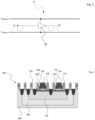
- Fig. 4 shows a cross-sectional view of the first logic gate 100 shown in Figs. 1 and 2 .
- the first transistors 110, 120 are implemented above a first secondary well 170, which is embedded in a deeper first primary well 160, which in turn is embedded in a substrate 500.
- a BOX layer 116, 126 has been provided between each first transistor 110, 120 and the first secondary well 170.
- the first secondary well 170 may act as the back gate for the first transistors 110, 120, as a voltage may be applied to the first secondary well 170 via the first secondary well contact 132.
- each first transistor 110, 120 may be implemented as known from MOSFET technology, by providing a gate electrode on the channel 119, 129 of a transistor, with a gate oxide layer 116, 126 separating the gate electrode and the channel.
- Fig. 5 shows an embodiment of the level shifter circuit 1 shown in Fig. 1 .
- the level shifter circuit shown in Fig. 4 differs in that latch circuit 2 comprises a different well configuration.
- the first logic gate 100 comprises a first primary well 160 embedded in the substrate and a first secondary well 170 embedded in the first primary well 160.
- the shown level shifter circuit 1 is implemented on a P-doped substrate so the first primary well 160 is an N-well and the first secondary well 170 is a P-well.
- the first logic gate 100 comprises a two first transistors 110, 120, one that is a PMOS transistor 110 and one that is an NMOS transistor 120.
- the PMOS transistor 110 is arranged on top of the first primary well 160 while the NMOS transistor 120 is arranged on top of the first secondary well 170.
- the first primary well 160 provides the back gate for the PMOS transistor 110
- the first secondary well 170 provides the back gate for the NMOS transistor 120.
- the first logic gate 100 comprises a first primary well contact 134, which couples the first primary well 160 to the first main input terminal 130, and a first secondary well contact 132, which couples the first secondary well 170 to the first main input terminal 130.
- the second logic gate 200 is symmetric to the first logic gate 100.
- the second logic gate 200 comprises a second primary well 260 embedded in the substrate and a second secondary well 270 embedded in the second primary well 260.
- the shown level shifter circuit 1 is implemented on a P-doped substrate so the second primary well 260 is an N-well and the second secondary well 270 is a P-well.
- the second logic gate 200 comprises a two second transistors 210, 220, one that is a PMOS transistor 210 and one that is an NMOS transistor 220.
- the PMOS transistor 210 is arranged on top of the second primary well 260 while the NMOS transistor 220 is arranged on top of the second secondary well 270.
- the second primary well 260 provides the back gate for the PMOS transistor 210
- the second secondary well 270 provides the back gate for the NMOS transistor 220.
- the second logic gate 200 comprises a second primary well contact 234, which couples the second primary well 260 to the second main input terminal 230, and a second secondary well contact 232, which couples the second secondary well 270 to the second main input terminal 230.
- both the NMOS transistors 120, 220 of the first and second logic gates 100, 200 and the PMOS transistors 110, 210 of the first and second logic gates 100, 200 retains regular threshold voltage, RVT.
- Fig. 6 shows a cross-sectional view of the first logic gate 100 of the embodiment shown in Fig. 5 .
- the first primary well 160 is embedded in the substrate 500, while the first secondary well 170 is embedded in the first primary well 160.
- the NMOS, first transistor 110 comprises a BOX layer 118 so as to separate the source, channel, and drain of the NMOS transistor 110 from the underlying first primary well 160.
- the PMOS, first transistor 120 also comprises a BOX layer 128 so as to separate the source, channel, and drain of the PMOS transistor 120 from the underlying first secondary well 160.
- Figs. 7a-d show four such configurations in a P-doped substrate 500.
- Fig. 7a shows the configuration used for the embodiment shown in Figs. 5 and 6 , where a P-type secondary well 170 and an N-doped primary well 160 is used.
- Fig. 7b shows an embodiment where a P-doped secondary well 170 is used as the back gate for the PMOS transistor and an N-doped primary well 160 is used as the back gate for the NMOS transistor, whereby both the PMOS and NMOS transistors becomes a low-threshold voltage, LVT.
- Fig. 7c shows the configuration used for the embodiment shown in Figs.
- a P-doped secondary well 170 embedded in an N-doped primary well 160 is used as the back gate for both the PMOS and NMOS transistors.
- Fig. 7d shows an embodiment where an N-doped primary well 160 is used as the back gate for both the PMOS and NMOS transistors and no secondary well is provided. It is noted that for embodiments with N-doped substrates all previously shown well configurations are possible if the primary wells are changed to P-wells and the secondary wells to N-wells. It is further noted, that a primary well may have multiple secondary wells embedded in it.
- Fig. 8 shows an embodiment using the well configuration of Fig. 7D . Other than the well configuration this embodiment is similar to the ones shown previously.
- Fig. 9 shows and embodiment similar to that shown in Fig. 8 but differing in that the input circuit 3 has a higher voltage than the first output voltage supply V DD,Output and second output voltage supply V SS,Output , i.e., V DD,Output ⁇ V SS,Input .
- an input circuit with higher voltage may be used for all embodiments including the ones previously described.
- Fig. 10 shows an embodiment of the level shifter circuit 1, wherein the first logic gate 100 and the second logic gate 200 are both inverters, e.g., as the embodiment shown in Fig. 8 .
- the first output terminal 150 is coupled to the second secondary input terminal 230, which is indicated by the line going from the output of the inverter symbol representing the inverter that is the first logic gate 100 to the input of the inverter symbol representing the inverter that is the second logic gate 200.
- second output terminal 250 is coupled to the first secondary input terminal 130, which is indicated by the line going from the output of the inverter symbol representing the inverter that is the second logic gate 200 to the input of the inverter symbol representing the inverter that is the first logic gate 100.
- the latch output terminal 300 is coupled to the output of the inverter that is the second logic gate 200, while the second latch output terminal 400 is coupled to the output of the inverter that is the first logic gate 200.
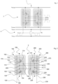
- Fig. 11a shows a multi-level shifter circuit according to the second aspect of the invention.
- the multi-level shifter circuit comprises multiple level shifter circuits, e.g., three level shifter circuits as shown, configured for shifting to different voltage domains 600, 602, 604, 606.
- Each level shifter circuit is similar to the one shown in Fig. 10 .
- each level shifter circuit comprises a first logic gate 100a, 100b, 100c and a second logic gate 200a, 200b, 200c, wherein the respective first logic gate 100a, 100b, 100c of each level shifter is cross-coupled to the respective second logic gate 200a, 200b, 200c of that level shifter as described for above.
- all of the first logic gates 100a, 100b, 100c have been arranged on top of the same first primary well 160 coupled to a first main input terminal 130 shared by the level shifter circuits. Thereby, the first primary well 160 provides the back gates for the first transistors of the level shifter circuits.
- all of the second logic gates 200a, 200b, 200c have been arranged on top of the same second primary well 260 coupled to a second main input terminal 230 shared by the level shifter circuits. Thereby, the second primary well 160 provides the back gates for the second transistors of the level shifter circuits.
- the implementation area can be reduced. It is noted, that the well configurations described above could also be used for one, more, or all of the first logic gates 100a, 100b, 100c, and/or for one, more, or all of the second logic gates 200a, 200b, 200c.
- each level shifter circuit shares its voltage supplies with its neighboring level shifter circuit, i.e., it shares its first output voltage supply V DD,Output with the level shifter circuit immediately above it, whereby the first output voltage supply V DD,Output also becomes the second output voltage supply V SS,Output for the level shifter circuit above it, and it shares its second output voltage supply V SS,Output with the level shifter circuit immediately below it, whereby the second output voltage supply V SS,Output also becomes the first output voltage supply V DD,Output for the level shifter circuit below it.
- the multi-level shifter circuit becomes more efficient as it reduces number of voltages supplies needed in the system.
- the voltage supplies have been provided with voltage values, which are merely exemplary for illustration.
- the second input voltage supply V SS,Output is 0V or ground, GND
- the first input voltage supply V DD,Output is 1.2V.
- the lowest voltage level shifter circuit has a second voltage supply 600 providing 2.1V and a first voltage supply 602 providing 2.8V.
- the middle voltage level shifter circuit has a second voltage supply 602 providing 2.8V and a first voltage supply 604 providing 3.5V.
- the high voltage level shifter circuit has a second voltage supply 604 providing 3.5V and a first voltage supply 606 providing 4.2V.
- Fig. 11b is a graph showing the output of the multi-level shifter circuit of Fig. 11a against the input. As is illustrated with the exemplary values it is possible for the level shifter and multi-level shifter circuit of the invention to perform voltage shifts of more than 3V, even with transistors that are only capable of withstanding voltages of around 1.5V on their front gate before being damaged.
- Fig. 12a show a hearing device 700, which in the shown embodiment is a RITE- or MaRie-type hearing aid.
- the hearing device 700 comprises a BTE component 702 adapted to be worn behind the ear of the user and an ITE component 704 adapted to be worn in the ear of the user.
- the hearing device comprises one or more input transducers 706, 708, e.g. one or more microphones and/or one or more bone vibration sensors, configured for capturing sound.
- the one or more input transducers may be arranged in the BTE component 702 and/or in the ITE component 704.
- the hearing device 702 comprises at least one output transducer, e.g. a loud speaker, which in the shown embodiment is arranged in the ITE component 704, but which may alternatively be arranged in the BTE component 702.
- Fig. 12b show a schematic view of the BTE component 702 of the hearing device 700 shown in Fig. 12a .
- the hearing device comprises two microphones 706, 708 connected to circuitry 710.
- the circuitry 712 comprises a processor adapted to process the signals representing the sound captured by the input transducers 706, 708.
- the BTE component 702 comprises an electrical interface 710 configured for being connected to the ITE component 704. Through the electrical interface 710, the circuitry 712 is connected to the output transducer, whereby processed signals may be sent to the output transducer and converted into an acoustic output.
- the hearing device 700 further comprises a power source 714 in the form of a battery, preferably a rechargeable battery.
- the power source 714 is connected to the circuitry 712 and used to power the hearing device 700.
- the battery can supply a first voltage, e.g. 4.2V.
- the circuitry 712 may comprise one or more voltage converters configured for converting the first voltage into one or more further voltages, e.g. 3.5V, 2.8V, 2.1V, and/or 1.2V. The first voltage and the further voltages may then be used for the various voltage supplies.
Landscapes
- Engineering & Computer Science (AREA)
- Computer Hardware Design (AREA)
- Physics & Mathematics (AREA)
- Computing Systems (AREA)
- General Engineering & Computer Science (AREA)
- Mathematical Physics (AREA)
- Acoustics & Sound (AREA)
- Signal Processing (AREA)
- Logic Circuits (AREA)
- Metal-Oxide And Bipolar Metal-Oxide Semiconductor Integrated Circuits (AREA)
Applications Claiming Priority (1)
| Application Number | Priority Date | Filing Date | Title |
|---|---|---|---|
| DKPA202200610 | 2022-06-24 |
Publications (2)
| Publication Number | Publication Date |
|---|---|
| EP4283872A2 true EP4283872A2 (de) | 2023-11-29 |
| EP4283872A3 EP4283872A3 (de) | 2024-01-03 |
Family
ID=86732855
Family Applications (1)
| Application Number | Title | Priority Date | Filing Date |
|---|---|---|---|
| EP23178166.7A Pending EP4283872A3 (de) | 2022-06-24 | 2023-06-08 | Pegelschieberschaltung mit durch backgate gesteuerten transistoren |
Country Status (3)
| Country | Link |
|---|---|
| US (1) | US20230421155A1 (de) |
| EP (1) | EP4283872A3 (de) |
| CN (1) | CN117294297A (de) |
Family Cites Families (13)
| Publication number | Priority date | Publication date | Assignee | Title |
|---|---|---|---|---|
| JP4030213B2 (ja) * | 1999-02-22 | 2008-01-09 | 株式会社ルネサステクノロジ | 半導体回路装置 |
| US7592841B2 (en) * | 2006-05-11 | 2009-09-22 | Dsm Solutions, Inc. | Circuit configurations having four terminal JFET devices |
| US8228092B2 (en) * | 2006-09-15 | 2012-07-24 | Texas Instruments Northern Virginia Incorporated | High voltage latching and DC restoration isolation and level shifting method and apparatus |
| US8289053B2 (en) * | 2008-07-30 | 2012-10-16 | Sharp Kabushiki Kaisha | Comparator circuit and display device provided with the same |
| US8258848B2 (en) * | 2010-09-07 | 2012-09-04 | Taiwan Semiconductor Manufacturing Co., Ltd. | Level shifter |
| WO2013018217A1 (ja) * | 2011-08-03 | 2013-02-07 | 富士通株式会社 | 半導体集積回路及びラッチ回路の駆動方法 |
| US9159402B2 (en) * | 2012-07-02 | 2015-10-13 | Stmicroelectronics International N.V. | SRAM bitcell implemented in double gate technology |
| DE102016115600B4 (de) * | 2016-08-23 | 2026-02-19 | Infineon Technologies Ag | Pegelumsetzer und verfahren zum betreiben von diesem |
| IT201600088225A1 (it) * | 2016-08-30 | 2018-03-02 | St Microelectronics Srl | Circuito traslatore di livello, in particolare per l'utilizzo in un dispositivo di memoria, e relativo dispositivo di memoria |
| CN121815845A (zh) * | 2019-01-29 | 2026-04-07 | 奥斯兰姆奥普托半导体股份有限两合公司 | 微型发光二极管、微型发光二极管装置、显示器及其方法 |
| EP4096078A1 (de) * | 2021-05-28 | 2022-11-30 | Oticon A/s | Hörgerät mit einer stromquelle |
| US12176025B2 (en) * | 2021-07-09 | 2024-12-24 | Stmicroelectronics International N.V. | Adaptive body bias management for an in-memory compute operation where simultaneous access is made to plural rows of a static random access memory (SRAM) |
| US11869623B2 (en) * | 2021-08-30 | 2024-01-09 | Taiwan Semiconductor Manufacturing Company, Ltd. | Latch type sense amplifier |
-
2023
- 2023-05-04 US US18/312,530 patent/US20230421155A1/en active Pending
- 2023-06-08 EP EP23178166.7A patent/EP4283872A3/de active Pending
- 2023-06-25 CN CN202310751746.5A patent/CN117294297A/zh active Pending
Also Published As
| Publication number | Publication date |
|---|---|
| CN117294297A (zh) | 2023-12-26 |
| EP4283872A3 (de) | 2024-01-03 |
| US20230421155A1 (en) | 2023-12-28 |
Similar Documents
| Publication | Publication Date | Title |
|---|---|---|
| KR100302535B1 (ko) | 가변 임계 전압을 가지는 soi형 반도체 장치 및 바이어스전압발생장치 | |
| US6326666B1 (en) | DTCMOS circuit having improved speed | |
| TWI481192B (zh) | 耐過壓之通過閘 | |
| EP1220450B1 (de) | Integrierte Halbleiterschaltung | |
| US6009021A (en) | MOS logic circuit with hold operation | |
| US6661253B1 (en) | Passgate structures for use in low-voltage applications | |
| CN110890886A (zh) | 超低电压数字电路的本体偏置 | |
| JP2010187122A (ja) | レベルシフタ回路 | |
| CN107888179A (zh) | 半导体装置 | |
| US6177811B1 (en) | Semiconductor integrated circuit device | |
| US9264045B2 (en) | Buffer circuit with reduced static leakage through controlled body biasing in FDSOI technology | |
| EP4283872A2 (de) | Pegelschieberschaltung mit durch backgate gesteuerten transistoren | |
| JP3730963B2 (ja) | 半導体集積回路 | |
| US7920019B2 (en) | Microprocessor with substrate bias clamps | |
| US8686882B2 (en) | High-frequency semiconductor switch and terminal device | |
| US10181855B2 (en) | Integrated circuit comprising adjustable back biasing of one or more logic circuit regions | |
| JPH11307652A (ja) | 論理演算回路 | |
| JP3547906B2 (ja) | 半導体集積回路装置 | |
| US20200099377A1 (en) | High speed buffer circuit | |
| CN116072667B (zh) | 用于宽电源电压范围的半导体器件结构 | |
| CN116339430B (zh) | 一种可耐极低负压的浮动衬底电压电路 | |
| KR101867510B1 (ko) | 정전기 방전 회로 | |
| JP2002368124A (ja) | 半導体装置 | |
| CN110708056B (zh) | 一种输入缓冲电路和输入缓冲方法 | |
| US20060181313A1 (en) | Transistor logic circuit |
Legal Events
| Date | Code | Title | Description |
|---|---|---|---|
| STAA | Information on the status of an ep patent application or granted ep patent |
Free format text: STATUS: UNKNOWN |
|
| PUAI | Public reference made under article 153(3) epc to a published international application that has entered the european phase |
Free format text: ORIGINAL CODE: 0009012 |
|
| STAA | Information on the status of an ep patent application or granted ep patent |
Free format text: STATUS: THE APPLICATION HAS BEEN PUBLISHED |
|
| AK | Designated contracting states |
Kind code of ref document: A2 Designated state(s): AL AT BE BG CH CY CZ DE DK EE ES FI FR GB GR HR HU IE IS IT LI LT LU LV MC ME MK MT NL NO PL PT RO RS SE SI SK SM TR |
|
| PUAL | Search report despatched |
Free format text: ORIGINAL CODE: 0009013 |
|
| AK | Designated contracting states |
Kind code of ref document: A3 Designated state(s): AL AT BE BG CH CY CZ DE DK EE ES FI FR GB GR HR HU IE IS IT LI LT LU LV MC ME MK MT NL NO PL PT RO RS SE SI SK SM TR |
|
| RIC1 | Information provided on ipc code assigned before grant |
Ipc: H03K 3/356 20060101AFI20231129BHEP |
|
| STAA | Information on the status of an ep patent application or granted ep patent |
Free format text: STATUS: REQUEST FOR EXAMINATION WAS MADE |
|
| 17P | Request for examination filed |
Effective date: 20240626 |
|
| RBV | Designated contracting states (corrected) |
Designated state(s): AL AT BE BG CH CY CZ DE DK EE ES FI FR GB GR HR HU IE IS IT LI LT LU LV MC ME MK MT NL NO PL PT RO RS SE SI SK SM TR |