EP4286931A2 - Dispositif d'affichage et son procédé de fabrication - Google Patents
Dispositif d'affichage et son procédé de fabrication Download PDFInfo
- Publication number
- EP4286931A2 EP4286931A2 EP23205122.7A EP23205122A EP4286931A2 EP 4286931 A2 EP4286931 A2 EP 4286931A2 EP 23205122 A EP23205122 A EP 23205122A EP 4286931 A2 EP4286931 A2 EP 4286931A2
- Authority
- EP
- European Patent Office
- Prior art keywords
- display device
- circuit board
- printed circuit
- guide
- flexible printed
- Prior art date
- Legal status (The legal status is an assumption and is not a legal conclusion. Google has not performed a legal analysis and makes no representation as to the accuracy of the status listed.)
- Granted
Links
Images




Classifications
-
- G—PHYSICS
- G09—EDUCATION; CRYPTOGRAPHY; DISPLAY; ADVERTISING; SEALS
- G09F—DISPLAYING; ADVERTISING; SIGNS; LABELS OR NAME-PLATES; SEALS
- G09F9/00—Indicating arrangements for variable information in which the information is built-up on a support by selection or combination of individual elements
- G09F9/30—Indicating arrangements for variable information in which the information is built-up on a support by selection or combination of individual elements in which the desired character or characters are formed by combining individual elements
- G09F9/301—Indicating arrangements for variable information in which the information is built-up on a support by selection or combination of individual elements in which the desired character or characters are formed by combining individual elements flexible foldable or roll-able electronic displays, e.g. thin LCD, OLED
-
- H—ELECTRICITY
- H10—SEMICONDUCTOR DEVICES; ELECTRIC SOLID-STATE DEVICES NOT OTHERWISE PROVIDED FOR
- H10K—ORGANIC ELECTRIC SOLID-STATE DEVICES
- H10K59/00—Integrated devices, or assemblies of multiple devices, comprising at least one organic light-emitting element covered by group H10K50/00
- H10K59/10—OLED displays
- H10K59/12—Active-matrix OLED [AMOLED] displays
- H10K59/129—Chiplets
-
- G—PHYSICS
- G02—OPTICS
- G02F—OPTICAL DEVICES OR ARRANGEMENTS FOR THE CONTROL OF LIGHT BY MODIFICATION OF THE OPTICAL PROPERTIES OF THE MEDIA OF THE ELEMENTS INVOLVED THEREIN; NON-LINEAR OPTICS; FREQUENCY-CHANGING OF LIGHT; OPTICAL LOGIC ELEMENTS; OPTICAL ANALOGUE/DIGITAL CONVERTERS
- G02F1/00—Devices or arrangements for the control of the intensity, colour, phase, polarisation or direction of light arriving from an independent light source, e.g. switching, gating or modulating; Non-linear optics
- G02F1/01—Devices or arrangements for the control of the intensity, colour, phase, polarisation or direction of light arriving from an independent light source, e.g. switching, gating or modulating; Non-linear optics for the control of the intensity, phase, polarisation or colour
- G02F1/13—Devices or arrangements for the control of the intensity, colour, phase, polarisation or direction of light arriving from an independent light source, e.g. switching, gating or modulating; Non-linear optics for the control of the intensity, phase, polarisation or colour based on liquid crystals, e.g. single liquid crystal display cells
- G02F1/133—Constructional arrangements; Operation of liquid crystal cells; Circuit arrangements
- G02F1/1333—Constructional arrangements; Manufacturing methods
- G02F1/133308—Support structures for LCD panels, e.g. frames or bezels
-
- G—PHYSICS
- G02—OPTICS
- G02B—OPTICAL ELEMENTS, SYSTEMS OR APPARATUS
- G02B6/00—Light guides; Structural details of arrangements comprising light guides and other optical elements, e.g. couplings
- G02B6/0001—Light guides; Structural details of arrangements comprising light guides and other optical elements, e.g. couplings specially adapted for lighting devices or systems
-
- G—PHYSICS
- G02—OPTICS
- G02F—OPTICAL DEVICES OR ARRANGEMENTS FOR THE CONTROL OF LIGHT BY MODIFICATION OF THE OPTICAL PROPERTIES OF THE MEDIA OF THE ELEMENTS INVOLVED THEREIN; NON-LINEAR OPTICS; FREQUENCY-CHANGING OF LIGHT; OPTICAL LOGIC ELEMENTS; OPTICAL ANALOGUE/DIGITAL CONVERTERS
- G02F1/00—Devices or arrangements for the control of the intensity, colour, phase, polarisation or direction of light arriving from an independent light source, e.g. switching, gating or modulating; Non-linear optics
- G02F1/01—Devices or arrangements for the control of the intensity, colour, phase, polarisation or direction of light arriving from an independent light source, e.g. switching, gating or modulating; Non-linear optics for the control of the intensity, phase, polarisation or colour
- G02F1/13—Devices or arrangements for the control of the intensity, colour, phase, polarisation or direction of light arriving from an independent light source, e.g. switching, gating or modulating; Non-linear optics for the control of the intensity, phase, polarisation or colour based on liquid crystals, e.g. single liquid crystal display cells
- G02F1/133—Constructional arrangements; Operation of liquid crystal cells; Circuit arrangements
- G02F1/1333—Constructional arrangements; Manufacturing methods
- G02F1/1345—Conductors connecting electrodes to cell terminals
- G02F1/13452—Conductors connecting driver circuitry and terminals of panels
-
- G—PHYSICS
- G06—COMPUTING OR CALCULATING; COUNTING
- G06F—ELECTRIC DIGITAL DATA PROCESSING
- G06F1/00—Details not covered by groups G06F3/00 - G06F13/00 and G06F21/00
- G06F1/16—Constructional details or arrangements
- G06F1/1613—Constructional details or arrangements for portable computers
- G06F1/1633—Constructional details or arrangements of portable computers not specific to the type of enclosures covered by groups G06F1/1615 - G06F1/1626
- G06F1/1637—Details related to the display arrangement, including those related to the mounting of the display in the housing
-
- H—ELECTRICITY
- H05—ELECTRIC TECHNIQUES NOT OTHERWISE PROVIDED FOR
- H05K—PRINTED CIRCUITS; CASINGS OR CONSTRUCTIONAL DETAILS OF ELECTRIC APPARATUS; MANUFACTURE OF ASSEMBLAGES OF ELECTRICAL COMPONENTS
- H05K1/00—Printed circuits
- H05K1/02—Details
- H05K1/0277—Bendability or stretchability details
-
- H—ELECTRICITY
- H05—ELECTRIC TECHNIQUES NOT OTHERWISE PROVIDED FOR
- H05K—PRINTED CIRCUITS; CASINGS OR CONSTRUCTIONAL DETAILS OF ELECTRIC APPARATUS; MANUFACTURE OF ASSEMBLAGES OF ELECTRICAL COMPONENTS
- H05K1/00—Printed circuits
- H05K1/02—Details
- H05K1/14—Structural association of two or more printed circuits
- H05K1/147—Structural association of two or more printed circuits at least one of the printed circuits being bent or folded, e.g. by using a flexible printed circuit
-
- H—ELECTRICITY
- H10—SEMICONDUCTOR DEVICES; ELECTRIC SOLID-STATE DEVICES NOT OTHERWISE PROVIDED FOR
- H10K—ORGANIC ELECTRIC SOLID-STATE DEVICES
- H10K50/00—Organic light-emitting devices
- H10K50/80—Constructional details
- H10K50/84—Passivation; Containers; Encapsulations
-
- H—ELECTRICITY
- H10—SEMICONDUCTOR DEVICES; ELECTRIC SOLID-STATE DEVICES NOT OTHERWISE PROVIDED FOR
- H10K—ORGANIC ELECTRIC SOLID-STATE DEVICES
- H10K50/00—Organic light-emitting devices
- H10K50/80—Constructional details
- H10K50/84—Passivation; Containers; Encapsulations
- H10K50/842—Containers
- H10K50/8426—Peripheral sealing arrangements, e.g. adhesives, sealants
-
- H—ELECTRICITY
- H10—SEMICONDUCTOR DEVICES; ELECTRIC SOLID-STATE DEVICES NOT OTHERWISE PROVIDED FOR
- H10K—ORGANIC ELECTRIC SOLID-STATE DEVICES
- H10K59/00—Integrated devices, or assemblies of multiple devices, comprising at least one organic light-emitting element covered by group H10K50/00
- H10K59/10—OLED displays
- H10K59/12—Active-matrix OLED [AMOLED] displays
- H10K59/131—Interconnections, e.g. wiring lines or terminals
-
- H—ELECTRICITY
- H10—SEMICONDUCTOR DEVICES; ELECTRIC SOLID-STATE DEVICES NOT OTHERWISE PROVIDED FOR
- H10K—ORGANIC ELECTRIC SOLID-STATE DEVICES
- H10K59/00—Integrated devices, or assemblies of multiple devices, comprising at least one organic light-emitting element covered by group H10K50/00
- H10K59/80—Constructional details
- H10K59/87—Passivation; Containers; Encapsulations
- H10K59/871—Self-supporting sealing arrangements
-
- H—ELECTRICITY
- H10—SEMICONDUCTOR DEVICES; ELECTRIC SOLID-STATE DEVICES NOT OTHERWISE PROVIDED FOR
- H10K—ORGANIC ELECTRIC SOLID-STATE DEVICES
- H10K59/00—Integrated devices, or assemblies of multiple devices, comprising at least one organic light-emitting element covered by group H10K50/00
- H10K59/80—Constructional details
- H10K59/87—Passivation; Containers; Encapsulations
- H10K59/871—Self-supporting sealing arrangements
- H10K59/8722—Peripheral sealing arrangements, e.g. adhesives, sealants
-
- H—ELECTRICITY
- H10—SEMICONDUCTOR DEVICES; ELECTRIC SOLID-STATE DEVICES NOT OTHERWISE PROVIDED FOR
- H10K—ORGANIC ELECTRIC SOLID-STATE DEVICES
- H10K59/00—Integrated devices, or assemblies of multiple devices, comprising at least one organic light-emitting element covered by group H10K50/00
- H10K59/80—Constructional details
- H10K59/87—Passivation; Containers; Encapsulations
- H10K59/873—Encapsulations
-
- H—ELECTRICITY
- H10—SEMICONDUCTOR DEVICES; ELECTRIC SOLID-STATE DEVICES NOT OTHERWISE PROVIDED FOR
- H10K—ORGANIC ELECTRIC SOLID-STATE DEVICES
- H10K71/00—Manufacture or treatment specially adapted for the organic devices covered by this subclass
-
- G—PHYSICS
- G02—OPTICS
- G02F—OPTICAL DEVICES OR ARRANGEMENTS FOR THE CONTROL OF LIGHT BY MODIFICATION OF THE OPTICAL PROPERTIES OF THE MEDIA OF THE ELEMENTS INVOLVED THEREIN; NON-LINEAR OPTICS; FREQUENCY-CHANGING OF LIGHT; OPTICAL LOGIC ELEMENTS; OPTICAL ANALOGUE/DIGITAL CONVERTERS
- G02F1/00—Devices or arrangements for the control of the intensity, colour, phase, polarisation or direction of light arriving from an independent light source, e.g. switching, gating or modulating; Non-linear optics
- G02F1/01—Devices or arrangements for the control of the intensity, colour, phase, polarisation or direction of light arriving from an independent light source, e.g. switching, gating or modulating; Non-linear optics for the control of the intensity, phase, polarisation or colour
- G02F1/13—Devices or arrangements for the control of the intensity, colour, phase, polarisation or direction of light arriving from an independent light source, e.g. switching, gating or modulating; Non-linear optics for the control of the intensity, phase, polarisation or colour based on liquid crystals, e.g. single liquid crystal display cells
- G02F1/133—Constructional arrangements; Operation of liquid crystal cells; Circuit arrangements
- G02F1/1333—Constructional arrangements; Manufacturing methods
- G02F1/133308—Support structures for LCD panels, e.g. frames or bezels
- G02F1/133314—Back frames
-
- G—PHYSICS
- G02—OPTICS
- G02F—OPTICAL DEVICES OR ARRANGEMENTS FOR THE CONTROL OF LIGHT BY MODIFICATION OF THE OPTICAL PROPERTIES OF THE MEDIA OF THE ELEMENTS INVOLVED THEREIN; NON-LINEAR OPTICS; FREQUENCY-CHANGING OF LIGHT; OPTICAL LOGIC ELEMENTS; OPTICAL ANALOGUE/DIGITAL CONVERTERS
- G02F1/00—Devices or arrangements for the control of the intensity, colour, phase, polarisation or direction of light arriving from an independent light source, e.g. switching, gating or modulating; Non-linear optics
- G02F1/01—Devices or arrangements for the control of the intensity, colour, phase, polarisation or direction of light arriving from an independent light source, e.g. switching, gating or modulating; Non-linear optics for the control of the intensity, phase, polarisation or colour
- G02F1/13—Devices or arrangements for the control of the intensity, colour, phase, polarisation or direction of light arriving from an independent light source, e.g. switching, gating or modulating; Non-linear optics for the control of the intensity, phase, polarisation or colour based on liquid crystals, e.g. single liquid crystal display cells
- G02F1/133—Constructional arrangements; Operation of liquid crystal cells; Circuit arrangements
- G02F1/1333—Constructional arrangements; Manufacturing methods
- G02F1/133308—Support structures for LCD panels, e.g. frames or bezels
- G02F1/133322—Mechanical guidance or alignment of LCD panel support components
-
- G—PHYSICS
- G02—OPTICS
- G02F—OPTICAL DEVICES OR ARRANGEMENTS FOR THE CONTROL OF LIGHT BY MODIFICATION OF THE OPTICAL PROPERTIES OF THE MEDIA OF THE ELEMENTS INVOLVED THEREIN; NON-LINEAR OPTICS; FREQUENCY-CHANGING OF LIGHT; OPTICAL LOGIC ELEMENTS; OPTICAL ANALOGUE/DIGITAL CONVERTERS
- G02F2201/00—Constructional arrangements not provided for in groups G02F1/00 - G02F7/00
- G02F2201/50—Protective arrangements
- G02F2201/503—Arrangements improving the resistance to shock
-
- H—ELECTRICITY
- H10—SEMICONDUCTOR DEVICES; ELECTRIC SOLID-STATE DEVICES NOT OTHERWISE PROVIDED FOR
- H10K—ORGANIC ELECTRIC SOLID-STATE DEVICES
- H10K77/00—Constructional details of devices covered by this subclass and not covered by groups H10K10/80, H10K30/80, H10K50/80 or H10K59/80
- H10K77/10—Substrates, e.g. flexible substrates
Definitions
- the present invention relates to a display device.
- Display devices are becoming increasingly important along with the development of multimedia.
- various types of display devices such as a liquid crystal display (LCD), an organic light emitting display (OLED) and the like have been used.
- Flexible display devices are shown in US 2016/363795 A1 , US 2015/253613 A1 , US 2005/241758 A1 , US 2014/307396 A1 and US 2016/179229 A1 .
- mobile electronic devices have been widely used.
- mobile electronic devices include tablet personal computers (PCs), in addition to small electronic devices such as mobile phones.
- PCs tablet personal computers
- small electronic devices such as mobile phones.
- the invention is realized by providing a display device including a support panel including a body and a guide, the guide being on one side of the body; a protective cap spaced apart from the guide at one side of the support panel; a first display substrate on the support panel; and a flexible printed circuit board on one side of the first display substrate, wherein an accommodation space is defined between the protective cap and the guide, and the flexible printed circuit board is accommodated in the accommodation space.
- a display device including a support panel including a body and a guide, the guide being on one side of the body; a protective cap spaced apart from the guide at one side of the support panel; a first display substrate on the support panel; and a flexible printed circuit board on one side of the first display substrate, wherein an accommodation space is defined between the protective cap and the guide, and the flexible printed circuit board is accommodated in the accommodation space.
- An alternative definition for the body and the guide of the support panel may be as follows:
- the support panel includes an end face which preferably has a curved form although also a flat form
- the end face may have a convex curved form, for example a parabolic form or the form of the segment of a circle or a U form.
- the protective cap may be spaced apart from the end face of the support panel. In so far, the guide may be also called end face.
- the flexible printed circuit board may include a bending area that is bent, and the bending area may be accommodated in the accommodation space.
- the display device may further include a driving chip on the flexible printed circuit board.
- An end of the protective cap may cover the driving chip.
- a central portion of the bending area may be spaced apart from the protective cap and the guide.
- the guide may include a protruding curved surface
- the protective cap may include a recessed curved surface corresponding to the protruding curved surface
- a cross-section of the accommodation space may have a laterally lying "U" shape.
- the display device may further include a protective film on an outside of the flexible printed circuit board.
- One end of the accommodation space is an open end and another end of the accommodation space is a closed end.
- the display device may further include a cover that covers the open end of the accommodation space.
- a thickness of the guide may be greater than a thickness of the body.
- the display device may further include a driving chip on the first display substrate.
- a central portion of the bending area may be spaced apart from the protective cap and the guide.
- the guide may include a protruding curved surface
- the protective cap may include a recessed curved surface corresponding to the protruding curved surface
- a thickness of the guide may be greater than a thickness of the body.
- the term "on” that is used to designate that an element is on another element or located on a different layer or a layer includes both a case where an element is located directly on another element or a layer and a case where an element is located on another element via another layer or still another element.
- first, second, and so forth are used to describe diverse constituent elements, such constituent elements are not limited by the terms. The terms are used only to discriminate a constituent element from other constituent elements. Accordingly, in the following description, a first constituent element may be a second constituent element.
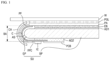
- FIG. 1 illustrates a cross-sectional view of a display device according to an embodiment of the present disclosure.
- FIG. 2 illustrates a partial perspective view of a display device according to an embodiment of the present disclosure.
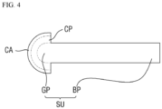
- FIGS. 3 and 4 illustrate side views of a display device according to an embodiment of the present disclosure.
- a display device may include a support panel SU including a body part or body BP and a guide part or guide GP (e.g., on one side of the body BP), a protective cap CA spaced apart from the guide GP at one side of the support panel SU, a first substrate PA on the support panel SU, and a flexible printed circuit board FPC on one side of the first substrate PA.
- the first substrate PA is a first display substrate PA.
- the support panel SU may have a plate shape and may provide a space where the first substrate PA to be described later is seated.
- the support panel SU may be made of, e.g., plastic or rubber. In an implementation, the support panel SU may be made of, e.g., a mixture of plastic and rubber, or may include other polymer materials.
- the support panel SU may be made of a material having elasticity. If the support panel SU is formed of a material having elasticity, the shock absorbing performance of the support panel SU may be improved.
- the support panel SU may include the body BP (having a plate shape) and the guide GP (on one side of the body BP).
- the guide GP may protrude from or at one side of the body BP.
- the guide GP may include a protruding curved surface that protrudes from or at one side of the body BP.
- an outer periphery of the cross section of the guide GP may include a curved line.
- the outer periphery of the cross section of the guide GP may have a parabolic shape lying laterally, e.g., may have a "C" shape.
- the guide GP may have a gentle curved surface to guide the flexible printed circuit board FPC such that the flexible printed circuit board FPC (described in greater detail below) can be disposed or accommodated stably. A detailed explanation will be given below.
- the guide GP and the body BP may be integrally formed (e.g., as a monolithic or one-piece structure).
- the guide GP and the body BP may be made of the same material.
- the guide GP and the body BP may be formed of different materials and may be formed independently of each other.
- a first adhesive layer AD1 may be disposed on the support panel SU.
- the first adhesive layer AD1 may at least partially cover the body BP of the support panel SU.
- the first adhesive layer AD1 may partially or entirely cover the body BP.
- the first adhesive layer AD1 may include a photocurable resin or thermosetting resin having high transmittance and adhesive performance.
- the first adhesive layer AD1 may be formed by applying a resin such as an acrylic resin and then curing the resin by irradiating ultraviolet rays (UV).
- the first adhesive layer AD1 may include an optically clear adhesive (OCA).
- a second substrate EN may be disposed on the first adhesive layer AD1.
- the second substrate EN may be an encapsulating substrate or an encapsulating film of an organic light emitting display device.
- the display device may be an organic light emitting display device.
- the first substrate PA may be disposed on the second substrate EN.
- the first substrate PA may be a TFT substrate on which a plurality of organic light emitting layers and a plurality of thin film transistors are disposed.
- the first substrate PA and the second substrate EN may be for suitable organic light emitting display devices, and therefore, a detailed description thereof may be omitted herein.
- the first substrate PA may be disposed on the second substrate EN.
- the stacking order may vary depending on the light emitting direction.
- the second substrate EN may be disposed on the first substrate PA (e.g., the first substrate PA may be between the support panel SU and the second substrate EN.
- the display device may be, e.g., an organic light emitting display device.
- the display device may be, e.g., a liquid crystal display device.
- a liquid crystal layer may be disposed between the first substrate PA and the second substrate EN.
- the order of stacking the first substrate PA and the second substrate EN may be changed as described above.
- the flexible printed circuit board FPC may be disposed on one side of the first substrate PA.
- the flexible printed circuit board FPC may be made of a thin film material. Accordingly, the flexible printed circuit board FPC may be bent or bendable.
- a bending area BA may be formed on or at the flexible printed circuit board FPC.
- the bending area BA may be defined as a non-zero curvature area in or of the flexible printed circuit board FPC.
- one end of the flexible printed circuit board FPC may be in contact with one end of the first substrate PA, and another end of the flexible printed circuit board FPC may be disposed below (e.g., spaced apart from and/or facing) the first substrate PA.
- a driving chip IC may be disposed on the flexible printed circuit board FPC.
- the driving chip IC may be a data driving integrated circuit.
- the driving chip IC may be a data driver that receives a data driving control signal and generates a data driving signal.
- the display device may be a chip on film (COF) type display device in which the driving chip IC is formed on the flexible printed circuit board FPC.
- COF chip on film
- a printed circuit board PCB may be disposed on the other end of the flexible printed circuit board FPC.
- the printed circuit board PCB may function as an external driving circuit and may be electrically connected to the flexible printed circuit board FPC.
- the printed circuit board PCB may include a driving circuit generating a driving signal for driving the display device or transmitting the generated driving signal.
- the printed circuit board PCB may generate a driving control signal controlling the driving chip IC disposed on the flexible printed circuit board FPC.
- the driving chip IC may generate a driving signal based on the driving control signal transmitted from the printed circuit board PCB and provide it to the display device.
- a second adhesive layer AD2 may be disposed between the other end of the flexible printed circuit board FPC and the support panel SU.
- the second adhesive layer AD2 may fix the flexible printed circuit board FPC and/or the printed circuit board PCB to the lower surface of the support panel SU. In this case, by fixing the other end of the flexible printed circuit board FPC, the bent state of the flexible printed circuit board FPC may be stably maintained.
- the second adhesive layer AD2 may be disposed at least partially on the lower surface of the support panel SU.
- the second adhesive layer AD2 may be formed partially or entirely on the lower surface of the support panel SU.
- the second adhesive layer AD2 may be partially formed on the lower surface of the support panel SU.
- a protective film PF may be disposed on an outside or outer side of the bending area BA of the flexible printed circuit board FPC.
- the bending area BA of the flexible printed circuit board FPC may be vulnerable to an external impact due to stress generated in the bent state.
- the protective film PF on the outside of the flexible printed circuit board FPC may help alleviate or otherwise compensate for an external impact, thereby preventing the bending area BA of the flexible printed circuit board FPC from being damaged.
- the protective film PF may be disposed on the outside of the flexible printed circuit board FPC. In an implementation, the protective film PF may be disposed on an inside or interior side of the flexible printed circuit board FPC, or may be disposed on both the inside and outside of the flexible printed circuit board FPC.
- the protective cap CA may be disposed at one side of the support panel SU.
- the protective cap CA may face the guide GP of the support panel SU.
- the protective cap CA may be spaced apart from the guide GP and may face the guide GP.
- the protective cap CA may include an inwardly curved (e.g., concave) surface.
- the protective cap CA may have a curved surface that is recessed inwardly to correspond to the protruding curved (e.g., convex) surface of the guide GP.
- the protective cap CA may have a concave structure that is roughly complementary to the convex structure of the guide GP.
- accommodation space AS When the protective cap CA and the guide GP are disposed to be spaced apart from each other by a predetermined distance, a separation space (hereinafter, referred to as “accommodation space AS") may be formed between the protective cap CA and the guide GP.
- a cross-section of the accommodation space AS may have a laterally lying "U” shape (e.g., a "C” shape). This may be a shape corresponding to the shape of the bending area BA of the flexible printed circuit board FPC described above.
- the accommodation space AS may extend in a longitudinal direction along the guide GP.
- FIG. 3 illustrates a side view seen from direction 1 of FIG. 2
- FIG. 4 illustrates a side view seen from direction 2 of FIG. 2 .
- an opening part or open end OP may be at one side or end of the accommodation space AS and a closing part or closed end CP may be at another side or end of the accommodation space AS.
- the closed end CP may be formed (e.g., the accommodation space AS may be closed off) by connecting the protective cap CA and the guide GP.
- a side wall connecting the protection cap CA and the guide GP may be formed at the other side or end of the accommodation space AS.
- the protective cap CA and the guide GP may be connected to each other by the side wall. Accordingly, the protective cap CA and the guide GP are separated from each other in the remaining portion (e.g., except for or other than the portion where the side wall is formed), so that the accommodation space AS can be formed (e.g., with the open end OP).
- the open end OP may be formed at one side of the accommodation space AS.
- the accommodation space AS may be connected to or in communication with an external space by the open end OP.
- the flexible printed circuit board FPC may be accommodated in the accommodation space AS through the open end OP.
- the flexible printed circuit board FPC may be accommodated in the accommodation space AS.
- the flexible printed circuit board FPC may be vulnerable to an external impact, and the flexible printed circuit board FPC may have minimal contact with the protective cap CA or the guide GP while being accommodated in the accommodation space AS.
- the bending area BA of the flexible printed circuit board FPC may maintain its shape by the elasticity of the material itself, and the accommodation space AS may accommodate the bending area BA of the flexible printed circuit board FPC so as to minimize contact therebetween, which may be advantageous in terms of durability.
- a central portion C of the bending area BA of the flexible printed circuit board FPC may not be in contact with the guide GP.
- the central portion C may be spaced apart from the guide GP.
- the central portion C of the bending area BA of the flexible printed circuit board FPC may also be spaced apart from the protective cap CA.
- the central portion C of the bending area BA may not be in contact with the guide GP and may not be in contact with the protective cap CA.
- the central portion C of the bending area BA may be not in contact with the guide GP and the protective cap CA, contact of the remaining portion of the bending area BA with the guide GP and the protective cap CA may be minimized. Accordingly, it is possible to help minimize the external impact transmitted to the flexible printed circuit board FPC through the guide GP and/or the protective cap CA.
- a polarizing plate POL may be disposed on the first substrate PA.
- the polarizing plate POL may be a circularly polarizing plate.
- the polarizing plate POL may include a ⁇ /4 phase retardation plate to help block or reflect light incident externally.
- the polarizing plate POL may be omitted.
- the polarizing plate POL may be a linearly polarizing plate that transmits light oscillating in one direction.
- a window W may be disposed on the polarizing plate POL.
- the window W may be also called window member.
- the window W may be formed of a transparent material that transmits light.
- the window may include, e.g., glass or transparent plastic.
- the window W may include a single layer.
- the window W may have a stacked structure in which a plurality of functional layers are stacked.
- the plurality of functional layers may include an adhesive layer or a bonding layer.
- the window W may have flexible properties.
- the window W may be formed of a bendable, foldable, rollable material or structure, and may be bent, folded, or rolled.
- the window W may have rigid properties. In this case, the window W may maintain an original shape as it is.
- FIG. 5 illustrates a cross-sectional view of a display device according to another embodiment of the present disclosure.
- the present embodiment is different from the embodiment of FIG. 1 in that a lower end of a protective cap CA1 may extend to a lower portion of the body BP of the support panel SU.
- the protective cap CA1 may be extend beyond the end face of the support panel SU and over the main surface of the support panel SU.
- the lower end (e.g., end distal to the first substrate PA) of the protective cap CA1 may extend to the inside of the display device.
- the protective cap CA1 can completely cover the driving chip IC.
- the protective cap CA1 may extend to at least partially cover the flexible printed circuit board FPC.
- the protective cap CA1 may extend to at least partially cover the printed circuit board PCB.
- the protective cap CA1 may extend to partially or completely cover the printed circuit board PCB.
- the protective cap CA1 may partially cover the printed circuit board PCB.
- FIG. 6 illustrates a cross-sectional view of a display device according to yet another embodiment of the present disclosure.
- the present embodiment is different from the embodiment of FIG. 1 in that the thickness of the guide GP is greater than the thickness of the body BP.
- the thickness direction is the stacking direction of the first substrate and the support panel, i.e. a direction as seen from the support panel to the first substrate, especially a direction perpendicular on the main surface of the support panel.
- the thickness of the guide GP may be greater than the thickness of the body BP (e.g., when measured in a same direction).
- the term "thickness" may mean the maximum thickness of a component.
- the guide GP may have a first thickness h1 and the body BP may have a second thickness h2.
- the first thickness h1 may be greater than the second thickness h2.
- a height difference may be formed in the support panel SU.
- protective layers PL1 and PL2 may be formed on an upper surface and/or a lower surface of the body BP.
- the protective layer on the upper surface of the body BP may be referred to as a first protective layer PL1
- the protective layer on the lower surface of the body BP may be referred to as a second protective layer PL2.
- the first protective layer PL1 and the second protective layer PL2 may compensate for the height difference.
- the first protective layer PL1 and the second protective layer PL2 may help mitigate or buffer impact.
- the first protective layer PL1 and/or the second protective layer PL2 may include a polymer resin.
- the first adhesive layer AD1 may be interposed between the first protective layer PL1 and the body BP and the second adhesive layer AD2 is interposed between the second protective layer PL2 and the body BP.
- the first protective layer PL1 may be disposed between the first adhesive layer AD1 and the body BP
- the second protective layer PL2 may be disposed between the second adhesive layer AD2 and the body BP.
- the first protective layer PL1 and the second protective layer PL2 may be omitted.
- the height difference may be compensated for by forming the first adhesive layer AD1 and the second adhesive layer AD2 to be relatively thick, for example with a thickness of the first adhesive layer AD1 and the second adhesive layer AD2 respectively corresponding to the step formed between the guide GP and the body BP on both sides of the support panel SU.
- the first adhesive layer AD1 and the second adhesive layer AD2 may be omitted.
- the height difference compensation may be performed by the first protective layer PL1 and the second protective layer PL2.
- FIG. 7 illustrates a partial perspective view of a display device according to still another embodiment of the present disclosure.
- the present embodiment is different from the embodiment of FIG. 3 in that the display device may include a cover CO that covers the open end OP of the accommodation space AS.
- the open end OP may be disposed at one side or end of the accommodation space AS and the closed end CP may be disposed at the other side or end of the accommodation space AS.
- the cover CO may cover the open end OP of the accommodation space AS while the flexible printed circuit board FPC is accommodated in the accommodation space AS.
- the cover CO covers the open end OP while the flexible printed circuit board FPC is accommodated in the accommodation space AS, it is possible to help prevent external contaminants and the like from entering the accommodation space AS.
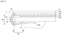
- FIG. 8 illustrates a cross-sectional view of a display device according to still another embodiment of the present disclosure.
- the present embodiment is different from the embodiment of FIG. 1 in that the flexible printed circuit board FPC is omitted and the bending area BA is formed on or at the first substrate PA1.
- the bending area BA may be formed on or at one side or part of the first substrate PA1.
- one side of the first substrate PA1 may be bent toward the inside of the first substrate PA1, e.g., toward a display region.
- the flexible printed circuit board FPC may be omitted.
- the driving chip IC may be directly mounted on one surface of the first substrate PA1.
- the display device may be a chip on panel (COP) type display device in which the driving chip IC is directly mounted on a display panel.
- COP chip on panel
- the display device according to the present embodiment may have substantially the same configuration as the above-described display device according to some embodiments of the present disclosure, except that the flexible printed circuit board FPC is omitted and the first substrate PA1 itself is bent.
- the protective cap CA1 as described in connection with FIG. 5 may be provided, especially to partially or completely cover the driving chip IC and to partially or completely cover the other structures as described in connection with FIG. 5 . Nevertheless, a redundant description thereof may be omitted.
- a method of manufacturing a display device may include a step of preparing or providing the support panel SU (including the body BP and the guide GP at on one side of the body BP), and providing the protective cap CA to face the guide GP at one side of the support panel SU, and a step of seating the first substrate PA (having the flexible printed circuit board FPC) on one side thereof on the support panel SU.
- the step of seating the first substrate PA on the support panel SU may include a step of inserting the bent flexible printed circuit board FPC into the accommodation space AS between the guide GP and the protective cap CA.
- a step of preparing or providing the support panel SU including the body BP and the guide GP (on one side of the body BP) may be performed and providing the protective cap CA to face the guide GP at one side of the support panel SU may be performed.
- the support panel SU and the protective cap CA may be substantially the same as those of the above-described display device according to some embodiments of the present disclosure.
- a step of seating the first substrate PA, on which the flexible printed circuit board FPC is formed at one end thereof, on the support panel SU may be performed.
- the step of seating the first substrate PA on the support panel SU may include a step of inserting the flexible printed circuit board FPC in a bent state into the accommodation space AS.
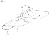
- FIG. 9 illustrates a partial perspective view of a method of manufacturing a display device according to an embodiment of the present disclosure.
- the flexible printed circuit board FPC in a bent state may be inserted into the open end OP of the accommodation space AS.
- the bending area BA of the flexible printed circuit board FPC may be inserted into the accommodation space AS.
- the flexible printed circuit board FPC (which has been partially inserted) may then be completely inserted by being slid along the accommodation space AS, so that the first substrate PA may be seated on the support panel SU.
- the flexible printed circuit board FPC may be omitted and the first substrate PA itself may be bent, see for example the first substrate PA1 of FIG. 8 .
- the bending area BA of the first substrate PA in a bent state may be inserted into the accommodation space AS.
- the bending area BA may be inserted into the accommodation space AS in substantially the same manner in which the flexible printed circuit board FPC is inserted as described above.
- the method of manufacturing a display device may further include a step of forming the first adhesive layer AD1 and/or the second adhesive layer AD2, a step of disposing the second substrate EN facing the first substrate PA, a step of forming the polarizing plate POL, a step of forming the window W, a step of forming the driving chip IC, and/or a step of forming the printed circuit board PCB.
- the first adhesive layer AD1, the second adhesive layer AD2, the second substrate EN, the polarizing plate POL, the window W, the driving chip IC, and the printed circuit board PCB may be substantially the same as those of the above-described display device according to some embodiments of the present disclosure.
- the forming method is not limited within the scope not departing from the above description.
- the step of forming the first adhesive layer AD1 and/or the second adhesive layer AD2, the step of disposing the second substrate EN facing the first substrate PA, the step of forming the polarizing plate POL, the step of forming the window W, the step of forming the driving chip IC, and/or the step of forming the printed circuit board PCB may be performed, without limiting their order, before, after or between the steps of the method of manufacturing a display device according to an embodiment of the present disclosure.
- the mobile electronic device may include a display device to provide visual information such as an image to a user.
- the display device may occupy a larger proportion of the electronic device.
- a structure in which a part of the display device may be bent to have a predetermined angle from a planar state may be considered.
- the embodiments may provide a display device capable of realizing a narrow bezel.
- the embodiments may provide a display device capable of realizing a narrow bezel while ensuing sufficient durability.
- the durability of the display device according to an embodiment may be improved.
Landscapes
- Physics & Mathematics (AREA)
- Engineering & Computer Science (AREA)
- Nonlinear Science (AREA)
- General Physics & Mathematics (AREA)
- Optics & Photonics (AREA)
- Theoretical Computer Science (AREA)
- Microelectronics & Electronic Packaging (AREA)
- Chemical & Material Sciences (AREA)
- Crystallography & Structural Chemistry (AREA)
- Mathematical Physics (AREA)
- Computer Hardware Design (AREA)
- Human Computer Interaction (AREA)
- General Engineering & Computer Science (AREA)
- Manufacturing & Machinery (AREA)
- Devices For Indicating Variable Information By Combining Individual Elements (AREA)
- Liquid Crystal (AREA)
Applications Claiming Priority (2)
| Application Number | Priority Date | Filing Date | Title |
|---|---|---|---|
| KR1020170004278A KR102646618B1 (ko) | 2017-01-11 | 2017-01-11 | 표시 장치 및 표시 장치의 제조 방법 |
| EP17208844.5A EP3349060B1 (fr) | 2017-01-11 | 2017-12-20 | Afficheur et son procédé de fabrication |
Related Parent Applications (1)
| Application Number | Title | Priority Date | Filing Date |
|---|---|---|---|
| EP17208844.5A Division EP3349060B1 (fr) | 2017-01-11 | 2017-12-20 | Afficheur et son procédé de fabrication |
Publications (3)
| Publication Number | Publication Date |
|---|---|
| EP4286931A2 true EP4286931A2 (fr) | 2023-12-06 |
| EP4286931A3 EP4286931A3 (fr) | 2024-02-21 |
| EP4286931B1 EP4286931B1 (fr) | 2024-12-11 |
Family
ID=60953549
Family Applications (2)
| Application Number | Title | Priority Date | Filing Date |
|---|---|---|---|
| EP23205122.7A Active EP4286931B1 (fr) | 2017-01-11 | 2017-12-20 | Dispositif d'affichage et son procédé de fabrication |
| EP17208844.5A Active EP3349060B1 (fr) | 2017-01-11 | 2017-12-20 | Afficheur et son procédé de fabrication |
Family Applications After (1)
| Application Number | Title | Priority Date | Filing Date |
|---|---|---|---|
| EP17208844.5A Active EP3349060B1 (fr) | 2017-01-11 | 2017-12-20 | Afficheur et son procédé de fabrication |
Country Status (4)
| Country | Link |
|---|---|
| US (1) | US10520762B2 (fr) |
| EP (2) | EP4286931B1 (fr) |
| KR (1) | KR102646618B1 (fr) |
| CN (1) | CN108305564B (fr) |
Families Citing this family (43)
| Publication number | Priority date | Publication date | Assignee | Title |
|---|---|---|---|---|
| KR102471758B1 (ko) * | 2017-12-11 | 2022-11-29 | 삼성디스플레이 주식회사 | 표시장치 |
| US10509278B2 (en) * | 2018-02-09 | 2019-12-17 | Wuhan China Star Optoelectronics Technology Co., Ltd. | Chip on film (COF) single-layer flexible printed circuit board and liquid crystal display (LCD) having the same |
| KR102543688B1 (ko) * | 2018-04-02 | 2023-06-14 | 삼성디스플레이 주식회사 | 표시 장치 및 표시 장치의 제조방법 |
| KR101934676B1 (ko) * | 2018-07-24 | 2019-01-03 | 주식회사 기가레인 | 벤딩 내구성이 향상된 전송선로 |
| KR102504397B1 (ko) * | 2018-08-20 | 2023-03-02 | 삼성디스플레이 주식회사 | 표시 장치 및 이를 이용한 전자장치 제조방법 |
| CN109148380B (zh) * | 2018-08-21 | 2021-02-02 | 武汉华星光电半导体显示技术有限公司 | 显示面板、显示模组以及电子装置 |
| CN109061879A (zh) * | 2018-08-22 | 2018-12-21 | Oppo广东移动通信有限公司 | 光投射器及其破裂的检测方法、深度相机和电子装置 |
| KR102630315B1 (ko) | 2018-10-24 | 2024-01-30 | 삼성디스플레이 주식회사 | 표시 장치 및 이를 이용한 전자장치 제조방법 |
| CN109375436B (zh) * | 2018-10-31 | 2020-09-08 | 武汉华星光电半导体显示技术有限公司 | 显示装置 |
| KR102672834B1 (ko) * | 2018-11-29 | 2024-06-05 | 엘지디스플레이 주식회사 | 플렉서블 표시장치 |
| JP2020101642A (ja) * | 2018-12-20 | 2020-07-02 | シャープ株式会社 | 表示装置および電子機器 |
| KR102657036B1 (ko) * | 2018-12-21 | 2024-04-11 | 엘지디스플레이 주식회사 | 표시 장치 |
| CN109541834B (zh) * | 2018-12-29 | 2021-11-02 | 厦门天马微电子有限公司 | 显示面板及显示装置 |
| CN111402725B (zh) * | 2019-01-03 | 2022-03-25 | 北京小米移动软件有限公司 | 可折叠设备及安装方法 |
| KR102381762B1 (ko) | 2019-02-21 | 2022-03-31 | 주식회사 엘지에너지솔루션 | 연성 인쇄 회로 기판을 덮는 보호 커버를 포함하는 전지 모듈 |
| CN110570753B (zh) * | 2019-09-17 | 2021-08-03 | 京东方科技集团股份有限公司 | 一种显示装置及其组装方法 |
| CN110658656B (zh) * | 2019-09-27 | 2022-05-13 | 京东方科技集团股份有限公司 | 一种显示面板、显示装置及显示面板的制备方法 |
| CN110596971B (zh) | 2019-09-27 | 2022-07-19 | 京东方科技集团股份有限公司 | 一种显示面板、显示装置及显示面板的制备方法 |
| KR102834211B1 (ko) * | 2019-10-25 | 2025-07-15 | 삼성디스플레이 주식회사 | 표시 장치 |
| US11563189B2 (en) * | 2020-03-06 | 2023-01-24 | Samsung Display Co., Ltd | Display device including bending protection and anti-reflection layers |
| FI20205672A1 (fi) * | 2020-06-25 | 2021-12-26 | Epec Oy | Elektroniikkalaite ja menetelmä elektroniikkalaitteen muodostamiseksi |
| CN113888959B (zh) * | 2020-07-03 | 2023-09-22 | Oppo广东移动通信有限公司 | 显示装置及其组装方法 |
| KR102771958B1 (ko) * | 2020-08-14 | 2025-02-24 | 삼성디스플레이 주식회사 | 표시 장치 및 이를 포함하는 타일형 표시 장치 |
| CN114120805B (zh) * | 2020-08-28 | 2025-03-18 | 京东方科技集团股份有限公司 | 显示装置、弯折垫片模组及其组装方法 |
| KR102861443B1 (ko) * | 2020-10-06 | 2025-09-18 | 엘지디스플레이 주식회사 | 표시장치 |
| CN114387874A (zh) * | 2020-10-21 | 2022-04-22 | 深圳市万普拉斯科技有限公司 | 柔性显示面板及移动终端 |
| CN114613256A (zh) * | 2020-12-09 | 2022-06-10 | 深圳市柔宇科技股份有限公司 | 一种柔性显示模组及电子设备 |
| CN112735273B (zh) * | 2020-12-30 | 2022-07-12 | 武汉华星光电半导体显示技术有限公司 | 一种显示屏及显示装置 |
| CN112863353A (zh) * | 2021-01-21 | 2021-05-28 | 深圳市伽弥科技有限公司 | 一种柔性透明屏的制作方法 |
| US12003019B2 (en) | 2021-02-25 | 2024-06-04 | Apple Inc. | Electronic device |
| US12213260B2 (en) * | 2021-02-25 | 2025-01-28 | Apple Inc. | Electronic device |
| CN113053246A (zh) * | 2021-03-12 | 2021-06-29 | 京东方科技集团股份有限公司 | 一种显示面板、显示装置 |
| CN113067141B (zh) * | 2021-04-02 | 2022-12-20 | 京东方科技集团股份有限公司 | 一种薄膜天线、显示模组及显示装置 |
| CN113257114B (zh) * | 2021-05-20 | 2022-06-10 | 武汉华星光电技术有限公司 | 显示装置及电子设备 |
| CN115484730A (zh) * | 2021-06-16 | 2022-12-16 | 北京小米移动软件有限公司 | 柔性电路板、制备方法、可动装置和电子设备 |
| CN113593411B (zh) * | 2021-07-30 | 2023-08-29 | 京东方科技集团股份有限公司 | 显示装置 |
| CN115843148B (zh) * | 2021-09-18 | 2024-07-02 | 荣耀终端有限公司 | 电路板组件以及电子设备 |
| JP7776966B2 (ja) * | 2021-11-01 | 2025-11-27 | シャープ株式会社 | 表示装置 |
| CN114023195B (zh) * | 2021-11-12 | 2023-07-04 | 昆山国显光电有限公司 | 显示模组、显示模组的控制方法 |
| KR102873685B1 (ko) | 2021-11-15 | 2025-10-17 | 엘지디스플레이 주식회사 | 디스플레이 장치 |
| KR102847580B1 (ko) | 2021-12-30 | 2025-08-18 | 엘지디스플레이 주식회사 | 디스플레이 장치 |
| CN114399950B (zh) * | 2022-01-19 | 2023-11-14 | 京东方科技集团股份有限公司 | 保护组件及显示装置 |
| CN117133185B (zh) * | 2023-09-12 | 2025-12-26 | 武汉天马微电子有限公司 | 一种显示装置 |
Citations (5)
| Publication number | Priority date | Publication date | Assignee | Title |
|---|---|---|---|---|
| US20050241758A1 (en) | 2004-01-07 | 2005-11-03 | Samsung Electronics Co., Ltd. | Bonding method of flexible film and display bonded thereby |
| US20140307396A1 (en) | 2013-04-10 | 2014-10-16 | Lg Display Co., Ltd. | Flexible display device and method of manufacturing the same |
| US20150253613A1 (en) | 2014-03-06 | 2015-09-10 | Samsung Display Co., Ltd. | Display apparatus |
| US20160179229A1 (en) | 2014-12-22 | 2016-06-23 | Lg Display Co., Ltd. | Flexible Organic Light Emitting Diode Display Device |
| US20160363795A1 (en) | 2015-06-10 | 2016-12-15 | Samsung Display Co., Ltd. | Display panel and display device including the same |
Family Cites Families (15)
| Publication number | Priority date | Publication date | Assignee | Title |
|---|---|---|---|---|
| JP3610077B2 (ja) * | 1992-03-26 | 2005-01-12 | セイコーエプソン株式会社 | 液晶表示装置および電子機器 |
| DE10123236A1 (de) * | 2001-05-12 | 2002-11-14 | Philips Corp Intellectual Pty | Plasmabildschirm mit blauem Leuchtstoff |
| CN1926926A (zh) * | 2004-04-06 | 2007-03-07 | 出光兴产株式会社 | 电极基板及其制造方法 |
| JP2008170691A (ja) * | 2007-01-11 | 2008-07-24 | Toshiba Matsushita Display Technology Co Ltd | 液晶表示装置 |
| JP2011003522A (ja) * | 2008-10-16 | 2011-01-06 | Semiconductor Energy Lab Co Ltd | フレキシブル発光装置、電子機器及びフレキシブル発光装置の作製方法 |
| KR20130015230A (ko) | 2011-08-02 | 2013-02-13 | 삼성디스플레이 주식회사 | 표시 장치 및 그 제조 방법 |
| US8804349B2 (en) * | 2012-10-19 | 2014-08-12 | Samsung Display Co., Ltd. | Foldable display device |
| KR101796813B1 (ko) * | 2013-02-01 | 2017-11-10 | 엘지디스플레이 주식회사 | 플렉서블 유기 발광 표시 장치 및 플렉서블 유기 발광 표시 장치의 제조 방법 |
| US9349969B2 (en) * | 2013-02-01 | 2016-05-24 | Lg Display Co., Ltd. | Electronic devices with flexible display and method for manufacturing the same |
| KR102009670B1 (ko) | 2013-02-28 | 2019-08-13 | 엘지디스플레이 주식회사 | 플렉서블 디스플레이 장치 및 그 제조 방법 |
| KR102046864B1 (ko) * | 2013-03-13 | 2019-11-20 | 삼성전자주식회사 | 유연성 디스플레이 장치 |
| CN105793772B (zh) * | 2013-11-21 | 2019-03-12 | 夏普株式会社 | 显示装置 |
| US9287329B1 (en) * | 2014-12-30 | 2016-03-15 | Lg Display Co., Ltd. | Flexible display device with chamfered polarization layer |
| US9933870B2 (en) * | 2015-03-17 | 2018-04-03 | Lg Display Co., Ltd. | Back plate member for flexible display, display apparatus including the same, and method of manufacturing the same |
| KR20170044803A (ko) * | 2015-10-15 | 2017-04-26 | 삼성디스플레이 주식회사 | 표시 장치 |
-
2017
- 2017-01-11 KR KR1020170004278A patent/KR102646618B1/ko active Active
- 2017-10-18 US US15/787,005 patent/US10520762B2/en active Active
- 2017-12-20 EP EP23205122.7A patent/EP4286931B1/fr active Active
- 2017-12-20 EP EP17208844.5A patent/EP3349060B1/fr active Active
-
2018
- 2018-01-08 CN CN201810014496.6A patent/CN108305564B/zh active Active
Patent Citations (5)
| Publication number | Priority date | Publication date | Assignee | Title |
|---|---|---|---|---|
| US20050241758A1 (en) | 2004-01-07 | 2005-11-03 | Samsung Electronics Co., Ltd. | Bonding method of flexible film and display bonded thereby |
| US20140307396A1 (en) | 2013-04-10 | 2014-10-16 | Lg Display Co., Ltd. | Flexible display device and method of manufacturing the same |
| US20150253613A1 (en) | 2014-03-06 | 2015-09-10 | Samsung Display Co., Ltd. | Display apparatus |
| US20160179229A1 (en) | 2014-12-22 | 2016-06-23 | Lg Display Co., Ltd. | Flexible Organic Light Emitting Diode Display Device |
| US20160363795A1 (en) | 2015-06-10 | 2016-12-15 | Samsung Display Co., Ltd. | Display panel and display device including the same |
Also Published As
| Publication number | Publication date |
|---|---|
| EP3349060B1 (fr) | 2023-11-22 |
| CN108305564A (zh) | 2018-07-20 |
| US20180196300A1 (en) | 2018-07-12 |
| EP4286931A3 (fr) | 2024-02-21 |
| US10520762B2 (en) | 2019-12-31 |
| EP3349060A1 (fr) | 2018-07-18 |
| KR102646618B1 (ko) | 2024-03-12 |
| KR20180083025A (ko) | 2018-07-20 |
| CN108305564B (zh) | 2021-10-26 |
| EP4286931B1 (fr) | 2024-12-11 |
Similar Documents
| Publication | Publication Date | Title |
|---|---|---|
| EP4286931B1 (fr) | Dispositif d'affichage et son procédé de fabrication | |
| US20240028169A1 (en) | Electronic device | |
| US10671124B2 (en) | Rollable display device | |
| US10651162B2 (en) | Display device with a chip on film | |
| US11107373B2 (en) | Flexible display device | |
| CN105976701B (zh) | 显示装置和便携式终端 | |
| US8659503B2 (en) | Multi-display apparatus having overlapping display panels | |
| US10908340B2 (en) | Display device | |
| US10003044B2 (en) | Cover window for a display device, and a display device including the same | |
| JP4738223B2 (ja) | 表示装置 | |
| CN110045530B (zh) | 显示装置 | |
| EP2547180B1 (fr) | Dispositif d'affichage à diode électroluminescente organique à matrice active de panneau d'écran tactile avec plaque de circuit imprimé flexible | |
| EP2778773B1 (fr) | Dispositif d'affichage flexible | |
| KR102776438B1 (ko) | 벤딩 영역에서 다른 두께를 가지는 보호층을 포함하는 디스플레이 및 이를 포함하는 플렉서블 전자 장치 | |
| US9913392B2 (en) | Flexible display stack-up and method for arranging | |
| EP3764196B1 (fr) | Afficheur | |
| US20140306942A1 (en) | Display apparatus | |
| US20120241774A1 (en) | Display module and manufacturing method thereof | |
| US20230350464A1 (en) | Display module | |
| CN112397667A (zh) | 显示装置 | |
| US7643106B2 (en) | Display module | |
| US12568747B2 (en) | Display device including display panel and imrpoved cover panel configuration | |
| US12513873B2 (en) | Display device | |
| US20240414993A1 (en) | Display device and manufacturing method thereof | |
| CN106066548A (zh) | 显示装置 |
Legal Events
| Date | Code | Title | Description |
|---|---|---|---|
| PUAI | Public reference made under article 153(3) epc to a published international application that has entered the european phase |
Free format text: ORIGINAL CODE: 0009012 |
|
| STAA | Information on the status of an ep patent application or granted ep patent |
Free format text: STATUS: THE APPLICATION HAS BEEN PUBLISHED |
|
| AC | Divisional application: reference to earlier application |
Ref document number: 3349060 Country of ref document: EP Kind code of ref document: P |
|
| AK | Designated contracting states |
Kind code of ref document: A2 Designated state(s): AL AT BE BG CH CY CZ DE DK EE ES FI FR GB GR HR HU IE IS IT LI LT LU LV MC MK MT NL NO PL PT RO RS SE SI SK SM TR |
|
| PUAL | Search report despatched |
Free format text: ORIGINAL CODE: 0009013 |
|
| AK | Designated contracting states |
Kind code of ref document: A3 Designated state(s): AL AT BE BG CH CY CZ DE DK EE ES FI FR GB GR HR HU IE IS IT LI LT LU LV MC MK MT NL NO PL PT RO RS SE SI SK SM TR |
|
| RIC1 | Information provided on ipc code assigned before grant |
Ipc: G02F 1/1345 20060101AFI20240117BHEP |
|
| STAA | Information on the status of an ep patent application or granted ep patent |
Free format text: STATUS: REQUEST FOR EXAMINATION WAS MADE |
|
| 17P | Request for examination filed |
Effective date: 20240322 |
|
| RBV | Designated contracting states (corrected) |
Designated state(s): AL AT BE BG CH CY CZ DE DK EE ES FI FR GB GR HR HU IE IS IT LI LT LU LV MC MK MT NL NO PL PT RO RS SE SI SK SM TR |
|
| GRAP | Despatch of communication of intention to grant a patent |
Free format text: ORIGINAL CODE: EPIDOSNIGR1 |
|
| STAA | Information on the status of an ep patent application or granted ep patent |
Free format text: STATUS: GRANT OF PATENT IS INTENDED |
|
| INTG | Intention to grant announced |
Effective date: 20240827 |
|
| GRAS | Grant fee paid |
Free format text: ORIGINAL CODE: EPIDOSNIGR3 |
|
| GRAA | (expected) grant |
Free format text: ORIGINAL CODE: 0009210 |
|
| STAA | Information on the status of an ep patent application or granted ep patent |
Free format text: STATUS: THE PATENT HAS BEEN GRANTED |
|
| AC | Divisional application: reference to earlier application |
Ref document number: 3349060 Country of ref document: EP Kind code of ref document: P |
|
| AK | Designated contracting states |
Kind code of ref document: B1 Designated state(s): AL AT BE BG CH CY CZ DE DK EE ES FI FR GB GR HR HU IE IS IT LI LT LU LV MC MK MT NL NO PL PT RO RS SE SI SK SM TR |
|
| REG | Reference to a national code |
Ref country code: GB Ref legal event code: FG4D |
|
| REG | Reference to a national code |
Ref country code: CH Ref legal event code: EP |
|
| REG | Reference to a national code |
Ref country code: DE Ref legal event code: R096 Ref document number: 602017086802 Country of ref document: DE |
|
| REG | Reference to a national code |
Ref country code: IE Ref legal event code: FG4D |
|
| REG | Reference to a national code |
Ref country code: NL Ref legal event code: FP |
|
| REG | Reference to a national code |
Ref country code: LT Ref legal event code: MG9D |
|
| PG25 | Lapsed in a contracting state [announced via postgrant information from national office to epo] |
Ref country code: HR Free format text: LAPSE BECAUSE OF FAILURE TO SUBMIT A TRANSLATION OF THE DESCRIPTION OR TO PAY THE FEE WITHIN THE PRESCRIBED TIME-LIMIT Effective date: 20241211 |
|
| PG25 | Lapsed in a contracting state [announced via postgrant information from national office to epo] |
Ref country code: FI Free format text: LAPSE BECAUSE OF FAILURE TO SUBMIT A TRANSLATION OF THE DESCRIPTION OR TO PAY THE FEE WITHIN THE PRESCRIBED TIME-LIMIT Effective date: 20241211 |
|
| PG25 | Lapsed in a contracting state [announced via postgrant information from national office to epo] |
Ref country code: BG Free format text: LAPSE BECAUSE OF FAILURE TO SUBMIT A TRANSLATION OF THE DESCRIPTION OR TO PAY THE FEE WITHIN THE PRESCRIBED TIME-LIMIT Effective date: 20241211 |
|
| PG25 | Lapsed in a contracting state [announced via postgrant information from national office to epo] |
Ref country code: ES Free format text: LAPSE BECAUSE OF FAILURE TO SUBMIT A TRANSLATION OF THE DESCRIPTION OR TO PAY THE FEE WITHIN THE PRESCRIBED TIME-LIMIT Effective date: 20241211 |
|
| PG25 | Lapsed in a contracting state [announced via postgrant information from national office to epo] |
Ref country code: NO Free format text: LAPSE BECAUSE OF FAILURE TO SUBMIT A TRANSLATION OF THE DESCRIPTION OR TO PAY THE FEE WITHIN THE PRESCRIBED TIME-LIMIT Effective date: 20250311 |
|
| PG25 | Lapsed in a contracting state [announced via postgrant information from national office to epo] |
Ref country code: LV Free format text: LAPSE BECAUSE OF FAILURE TO SUBMIT A TRANSLATION OF THE DESCRIPTION OR TO PAY THE FEE WITHIN THE PRESCRIBED TIME-LIMIT Effective date: 20241211 Ref country code: GR Free format text: LAPSE BECAUSE OF FAILURE TO SUBMIT A TRANSLATION OF THE DESCRIPTION OR TO PAY THE FEE WITHIN THE PRESCRIBED TIME-LIMIT Effective date: 20250312 |
|
| PG25 | Lapsed in a contracting state [announced via postgrant information from national office to epo] |
Ref country code: RS Free format text: LAPSE BECAUSE OF FAILURE TO SUBMIT A TRANSLATION OF THE DESCRIPTION OR TO PAY THE FEE WITHIN THE PRESCRIBED TIME-LIMIT Effective date: 20250311 |
|
| REG | Reference to a national code |
Ref country code: AT Ref legal event code: MK05 Ref document number: 1750862 Country of ref document: AT Kind code of ref document: T Effective date: 20241211 |
|
| PG25 | Lapsed in a contracting state [announced via postgrant information from national office to epo] |
Ref country code: SM Free format text: LAPSE BECAUSE OF FAILURE TO SUBMIT A TRANSLATION OF THE DESCRIPTION OR TO PAY THE FEE WITHIN THE PRESCRIBED TIME-LIMIT Effective date: 20241211 |
|
| PG25 | Lapsed in a contracting state [announced via postgrant information from national office to epo] |
Ref country code: PL Free format text: LAPSE BECAUSE OF FAILURE TO SUBMIT A TRANSLATION OF THE DESCRIPTION OR TO PAY THE FEE WITHIN THE PRESCRIBED TIME-LIMIT Effective date: 20241211 |
|
| PG25 | Lapsed in a contracting state [announced via postgrant information from national office to epo] |
Ref country code: IS Free format text: LAPSE BECAUSE OF FAILURE TO SUBMIT A TRANSLATION OF THE DESCRIPTION OR TO PAY THE FEE WITHIN THE PRESCRIBED TIME-LIMIT Effective date: 20250411 |
|
| PG25 | Lapsed in a contracting state [announced via postgrant information from national office to epo] |
Ref country code: PT Free format text: LAPSE BECAUSE OF FAILURE TO SUBMIT A TRANSLATION OF THE DESCRIPTION OR TO PAY THE FEE WITHIN THE PRESCRIBED TIME-LIMIT Effective date: 20250411 |
|
| PG25 | Lapsed in a contracting state [announced via postgrant information from national office to epo] |
Ref country code: EE Free format text: LAPSE BECAUSE OF FAILURE TO SUBMIT A TRANSLATION OF THE DESCRIPTION OR TO PAY THE FEE WITHIN THE PRESCRIBED TIME-LIMIT Effective date: 20241211 |
|
| PG25 | Lapsed in a contracting state [announced via postgrant information from national office to epo] |
Ref country code: RO Free format text: LAPSE BECAUSE OF FAILURE TO SUBMIT A TRANSLATION OF THE DESCRIPTION OR TO PAY THE FEE WITHIN THE PRESCRIBED TIME-LIMIT Effective date: 20241211 Ref country code: AT Free format text: LAPSE BECAUSE OF FAILURE TO SUBMIT A TRANSLATION OF THE DESCRIPTION OR TO PAY THE FEE WITHIN THE PRESCRIBED TIME-LIMIT Effective date: 20241211 |
|
| PG25 | Lapsed in a contracting state [announced via postgrant information from national office to epo] |
Ref country code: SK Free format text: LAPSE BECAUSE OF FAILURE TO SUBMIT A TRANSLATION OF THE DESCRIPTION OR TO PAY THE FEE WITHIN THE PRESCRIBED TIME-LIMIT Effective date: 20241211 |
|
| PG25 | Lapsed in a contracting state [announced via postgrant information from national office to epo] |
Ref country code: CZ Free format text: LAPSE BECAUSE OF FAILURE TO SUBMIT A TRANSLATION OF THE DESCRIPTION OR TO PAY THE FEE WITHIN THE PRESCRIBED TIME-LIMIT Effective date: 20241211 |
|
| PG25 | Lapsed in a contracting state [announced via postgrant information from national office to epo] |
Ref country code: IT Free format text: LAPSE BECAUSE OF FAILURE TO SUBMIT A TRANSLATION OF THE DESCRIPTION OR TO PAY THE FEE WITHIN THE PRESCRIBED TIME-LIMIT Effective date: 20241211 |
|
| REG | Reference to a national code |
Ref country code: CH Ref legal event code: PL |
|
| PG25 | Lapsed in a contracting state [announced via postgrant information from national office to epo] |
Ref country code: LU Free format text: LAPSE BECAUSE OF NON-PAYMENT OF DUE FEES Effective date: 20241220 |
|
| PG25 | Lapsed in a contracting state [announced via postgrant information from national office to epo] |
Ref country code: SE Free format text: LAPSE BECAUSE OF FAILURE TO SUBMIT A TRANSLATION OF THE DESCRIPTION OR TO PAY THE FEE WITHIN THE PRESCRIBED TIME-LIMIT Effective date: 20241211 |
|
| REG | Reference to a national code |
Ref country code: DE Ref legal event code: R097 Ref document number: 602017086802 Country of ref document: DE |
|
| PG25 | Lapsed in a contracting state [announced via postgrant information from national office to epo] |
Ref country code: MC Free format text: LAPSE BECAUSE OF FAILURE TO SUBMIT A TRANSLATION OF THE DESCRIPTION OR TO PAY THE FEE WITHIN THE PRESCRIBED TIME-LIMIT Effective date: 20241211 |
|
| REG | Reference to a national code |
Ref country code: BE Ref legal event code: MM Effective date: 20241231 |
|
| PG25 | Lapsed in a contracting state [announced via postgrant information from national office to epo] |
Ref country code: DK Free format text: LAPSE BECAUSE OF FAILURE TO SUBMIT A TRANSLATION OF THE DESCRIPTION OR TO PAY THE FEE WITHIN THE PRESCRIBED TIME-LIMIT Effective date: 20241211 |
|
| PG25 | Lapsed in a contracting state [announced via postgrant information from national office to epo] |
Ref country code: BE Free format text: LAPSE BECAUSE OF NON-PAYMENT OF DUE FEES Effective date: 20241231 |
|
| PLBE | No opposition filed within time limit |
Free format text: ORIGINAL CODE: 0009261 |
|
| STAA | Information on the status of an ep patent application or granted ep patent |
Free format text: STATUS: NO OPPOSITION FILED WITHIN TIME LIMIT |
|
| PG25 | Lapsed in a contracting state [announced via postgrant information from national office to epo] |
Ref country code: CH Free format text: LAPSE BECAUSE OF NON-PAYMENT OF DUE FEES Effective date: 20241231 |
|
| PG25 | Lapsed in a contracting state [announced via postgrant information from national office to epo] |
Ref country code: IE Free format text: LAPSE BECAUSE OF NON-PAYMENT OF DUE FEES Effective date: 20241220 |
|
| 26N | No opposition filed |
Effective date: 20250912 |
|
| PGFP | Annual fee paid to national office [announced via postgrant information from national office to epo] |
Ref country code: NL Payment date: 20251120 Year of fee payment: 9 |
|
| PGFP | Annual fee paid to national office [announced via postgrant information from national office to epo] |
Ref country code: DE Payment date: 20251120 Year of fee payment: 9 |
|
| PGFP | Annual fee paid to national office [announced via postgrant information from national office to epo] |
Ref country code: GB Payment date: 20251120 Year of fee payment: 9 |
|
| PGFP | Annual fee paid to national office [announced via postgrant information from national office to epo] |
Ref country code: FR Payment date: 20251125 Year of fee payment: 9 |